EP0121271A1 - Elektronischer Baustein - Google Patents
Elektronischer Baustein Download PDFInfo
- Publication number
- EP0121271A1 EP0121271A1 EP84200215A EP84200215A EP0121271A1 EP 0121271 A1 EP0121271 A1 EP 0121271A1 EP 84200215 A EP84200215 A EP 84200215A EP 84200215 A EP84200215 A EP 84200215A EP 0121271 A1 EP0121271 A1 EP 0121271A1
- Authority
- EP
- European Patent Office
- Prior art keywords
- positions
- spin
- magnetic
- charge carriers
- layer
- Prior art date
- Legal status (The legal status is an assumption and is not a legal conclusion. Google has not performed a legal analysis and makes no representation as to the accuracy of the status listed.)
- Granted
Links
Images
Classifications
-
- H—ELECTRICITY
- H01—ELECTRIC ELEMENTS
- H01F—MAGNETS; INDUCTANCES; TRANSFORMERS; SELECTION OF MATERIALS FOR THEIR MAGNETIC PROPERTIES
- H01F1/00—Magnets or magnetic bodies characterised by the magnetic materials therefor; Selection of materials for their magnetic properties
- H01F1/01—Magnets or magnetic bodies characterised by the magnetic materials therefor; Selection of materials for their magnetic properties of inorganic materials
- H01F1/40—Magnets or magnetic bodies characterised by the magnetic materials therefor; Selection of materials for their magnetic properties of inorganic materials of magnetic semiconductor materials, e.g. CdCr2S4
-
- H—ELECTRICITY
- H10—SEMICONDUCTOR DEVICES; ELECTRIC SOLID-STATE DEVICES NOT OTHERWISE PROVIDED FOR
- H10N—ELECTRIC SOLID-STATE DEVICES NOT OTHERWISE PROVIDED FOR
- H10N50/00—Galvanomagnetic devices
- H10N50/10—Magnetoresistive devices
-
- H—ELECTRICITY
- H10—SEMICONDUCTOR DEVICES; ELECTRIC SOLID-STATE DEVICES NOT OTHERWISE PROVIDED FOR
- H10N—ELECTRIC SOLID-STATE DEVICES NOT OTHERWISE PROVIDED FOR
- H10N50/00—Galvanomagnetic devices
- H10N50/20—Spin-polarised current-controlled devices
-
- H—ELECTRICITY
- H10—SEMICONDUCTOR DEVICES; ELECTRIC SOLID-STATE DEVICES NOT OTHERWISE PROVIDED FOR
- H10N—ELECTRIC SOLID-STATE DEVICES NOT OTHERWISE PROVIDED FOR
- H10N50/00—Galvanomagnetic devices
- H10N50/80—Constructional details
- H10N50/85—Materials of the active region
Definitions
- This invention relates to a new type of material, which material can be designated as a semi-metallic ferro- magnet, and also relates to a device in which such a material is employed.
- the invention is concerned with a material which, according to the above classification,can be characterized as a semi-metallic ferromagnetic or ferrimagnetic material.
- such a material which according to the invention is characterized by a crystal structure in which the occupation of the positions in the crystal lattice by the different elements, and the choice of these elements for these positions are such that, in one direction of magnetic polarization, the material exhibits all properties of a metal as regards the transport of electrons with a given-direction of spin, while for electrons of opposite magnetic spin the material exhibits all properties of a semi-conductive material or an insulator, opens up a route to a wholly new class of electronic devices.
- a layer of the material according to the invention only conducts charge carriers (for example electrons) with one specific direction of spin, such a layer can be used as a filter to produce polarized particles (such as electrons).
- the material can be made into polarizers and analyzers for such particles in analogy to a nicol or polaroid filter for light.
- At least one of the elements constituting the material is a magnetic atom, with the crystal structure being such that, at that position, it does not exhibit inversion symmetry.
- the magnetic atom is preferably manganese.
- the crystal structure is a so-called C1 - Heusler 2 structure that can be described as space group F 4 3 m (T d) (number 216 in the International Tables for X-ray Diffraction), and in which the a-positions (0,0,0) are occupied by an element from the third part of Group VIII of the Periodic Table (Ni, Pd, Pt), the b-positions (1 ⁇ 2,1 ⁇ 2,1 ⁇ 2) are unoccupied, the c-positions (1 ⁇ 4,1 ⁇ 4,1 ⁇ 4) are occupied by a magnetic element, and the d-positions (3/4,3/4,3/4) are occupied by an element of Group Va of the Periodic Table.
- T d space group F 4 3 m
- a highly suitable material of this preferred type is one in which the a-positions are occupied by nickel atoms, the c-positions by manganese atoms, and the d-positions by antimony atoms.
- a general characteristic of such devices is that they comprise a plurality of layers of crystalline material, and include means for injecting charge carriers into at least one of the layers and for removing charge carriers from at least one other layer, characterized in that at least one of the layers is a material according to the invention, and that one layer is arranged as an area. for affecting the direction of spin of charge carriers moving in the device.
- said at least one layer of the material according to the invention consists in essence of a single magnetic domain.
- an external influence may be an electrical, a magnetic, or an electro-magnetic vibration (light or micro-wave).
- the external influence may even be a mechanical vibration, such as sound, while influencing by temperature is among the possibilities.
- a substantial advantage of the material according to the invention and the devices based on it is that the speed of operation is equal to the speed with which basic physical phenomena take place. Influencing the spin orientation of a charge carrier, for example, reversing the spin orientation of an electron, takes place at a speed of 10 -11 second. This, then, is also the order of velocity at which a device according to the invention can operate, which is a factor of 100 faster than devices hitherto known.
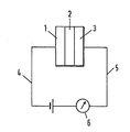
- the device shown diagrammatically, consists in essence of three layers.
- Layer 1 consists of the material according to the invention, for example,Ni Mn Sb, magnetized in one direction.
- Layer 2 consists of a suitable material in which the spin orientation of charge carriers moving therein can be influenced. Examples of such materials are the rare earth metals and the so-called transition metals.
- Layer 3 consists again of the material according to the invention. Layers 1 and 3 may be very thin, so long as a homogeneous magnetizable layer is available. A thickness in the order of 100 atoms is already sufficient.
- a conductor 4 Connected to layer 1 is a conductor 4 supplying charge carriers to the device, and connected to layer 3 is a conductor 5 for the removal of charge carriers.
- the device operates as a conductor for such charge carriers.
- Charge carriers with a downward spin (“spin-down") are not passed, because layers 1 and 3 operate as insulators for such charge carriers.
- the device can serve both as a source of polarized charge carriers and for detecting an external influence.
- the passage of charge carriers by the device can be indicated, for example, by an ammeter 6 connected to conductor 5.
Landscapes
- Engineering & Computer Science (AREA)
- Power Engineering (AREA)
- Hall/Mr Elements (AREA)
- Soft Magnetic Materials (AREA)
- Hard Magnetic Materials (AREA)
- Magnetic Ceramics (AREA)
- Superconductors And Manufacturing Methods Therefor (AREA)
- Glass Compositions (AREA)
- Surgical Instruments (AREA)
- Valve Device For Special Equipments (AREA)
- Noodles (AREA)
Priority Applications (1)
| Application Number | Priority Date | Filing Date | Title |
|---|---|---|---|
| AT84200215T ATE34882T1 (de) | 1983-02-17 | 1984-02-17 | Elektronischer baustein. |
Applications Claiming Priority (2)
| Application Number | Priority Date | Filing Date | Title |
|---|---|---|---|
| NL8300602A NL8300602A (nl) | 1983-02-17 | 1983-02-17 | Half-metallisch ferro- resp. ferrimagnetisch materiaal en inrichting waarin dergelijk materiaal wordt toegepast. |
| NL8300602 | 1983-02-17 |
Publications (2)
| Publication Number | Publication Date |
|---|---|
| EP0121271A1 true EP0121271A1 (de) | 1984-10-10 |
| EP0121271B1 EP0121271B1 (de) | 1988-06-01 |
Family
ID=19841435
Family Applications (1)
| Application Number | Title | Priority Date | Filing Date |
|---|---|---|---|
| EP84200215A Expired EP0121271B1 (de) | 1983-02-17 | 1984-02-17 | Elektronischer Baustein |
Country Status (10)
| Country | Link |
|---|---|
| EP (1) | EP0121271B1 (de) |
| JP (1) | JPS6035587A (de) |
| AT (1) | ATE34882T1 (de) |
| AU (1) | AU2465484A (de) |
| CA (1) | CA1216375A (de) |
| DE (1) | DE3471836D1 (de) |
| DK (1) | DK72984A (de) |
| IE (1) | IE55211B1 (de) |
| NL (1) | NL8300602A (de) |
| NO (1) | NO840589L (de) |
Cited By (2)
| Publication number | Priority date | Publication date | Assignee | Title |
|---|---|---|---|---|
| EP0524369A3 (en) * | 1991-07-03 | 1993-04-07 | International Business Machines Corporation | Novel device for selective magnetization and method |
| WO1996007208A1 (en) * | 1994-08-31 | 1996-03-07 | Douwe Johannes Monsma | Current conducting structure with at least one potential barrier and method of manufcturing such |
Citations (2)
| Publication number | Priority date | Publication date | Assignee | Title |
|---|---|---|---|---|
| US3840865A (en) * | 1972-06-23 | 1974-10-08 | Ibm | Detection of magnetic domains by tunnel junctions |
| US3972035A (en) * | 1972-06-23 | 1976-07-27 | International Business Machines Corporation | Detection of magnetic domains by tunnel junctions |
Family Cites Families (1)
| Publication number | Priority date | Publication date | Assignee | Title |
|---|---|---|---|---|
| DE2215878A1 (de) * | 1972-03-30 | 1973-12-06 | Siemens Ag | Magnetisch steuerbares festkoerperschaltelement |
-
1983
- 1983-02-17 NL NL8300602A patent/NL8300602A/nl not_active Application Discontinuation
-
1984
- 1984-02-16 AU AU24654/84A patent/AU2465484A/en not_active Abandoned
- 1984-02-16 NO NO840589A patent/NO840589L/no unknown
- 1984-02-16 CA CA000447599A patent/CA1216375A/en not_active Expired
- 1984-02-17 IE IE368/84A patent/IE55211B1/en unknown
- 1984-02-17 EP EP84200215A patent/EP0121271B1/de not_active Expired
- 1984-02-17 DE DE8484200215T patent/DE3471836D1/de not_active Expired
- 1984-02-17 DK DK72984A patent/DK72984A/da not_active Application Discontinuation
- 1984-02-17 AT AT84200215T patent/ATE34882T1/de not_active IP Right Cessation
- 1984-02-17 JP JP59028429A patent/JPS6035587A/ja active Pending
Patent Citations (2)
| Publication number | Priority date | Publication date | Assignee | Title |
|---|---|---|---|---|
| US3840865A (en) * | 1972-06-23 | 1974-10-08 | Ibm | Detection of magnetic domains by tunnel junctions |
| US3972035A (en) * | 1972-06-23 | 1976-07-27 | International Business Machines Corporation | Detection of magnetic domains by tunnel junctions |
Non-Patent Citations (2)
| Title |
|---|
| LANDOLT-BÖRNSTEIN: "Zahlenwerk und Funktionen aus Physik, Chemie, Astronomie, Geophysik und Technik", 6th edition, vol. II, pages 3-75 - 3-76; "Eigenschaften der Materie in ihren Aggregatzuständen"; part 9, "Magnetische Eigenschaften I" * |
| SIEMENS FORSCHUNGS- UND ENTWICKLUNGSBERICHTE, vol. 1, no. 4, 1972, pages 369-375, Springer-Verlag, DE W. LUGSCHNEIDER et al.: "Magnetic semiconductors" * |
Cited By (2)
| Publication number | Priority date | Publication date | Assignee | Title |
|---|---|---|---|---|
| EP0524369A3 (en) * | 1991-07-03 | 1993-04-07 | International Business Machines Corporation | Novel device for selective magnetization and method |
| WO1996007208A1 (en) * | 1994-08-31 | 1996-03-07 | Douwe Johannes Monsma | Current conducting structure with at least one potential barrier and method of manufcturing such |
Also Published As
| Publication number | Publication date |
|---|---|
| DE3471836D1 (en) | 1988-07-07 |
| EP0121271B1 (de) | 1988-06-01 |
| IE55211B1 (en) | 1990-07-04 |
| CA1216375A (en) | 1987-01-06 |
| JPS6035587A (ja) | 1985-02-23 |
| NO840589L (no) | 1984-08-20 |
| AU2465484A (en) | 1984-08-23 |
| IE840368L (en) | 1984-08-17 |
| DK72984D0 (da) | 1984-02-17 |
| NL8300602A (nl) | 1984-09-17 |
| ATE34882T1 (de) | 1988-06-15 |
| DK72984A (da) | 1984-08-18 |
Similar Documents
| Publication | Publication Date | Title |
|---|---|---|
| Kao | Dielectric phenomena in solids | |
| Pickett | Single spin superconductivity | |
| Mott | On the transition to metallic conduction in semiconductors | |
| Tsymbal et al. | Modelling of spin-polarized electron tunnelling from 3d ferromagnets | |
| US5936293A (en) | Hard/soft magnetic tunnel junction device with stable hard ferromagnetic layer | |
| Reisinger et al. | Hall effect, magnetization, and conductivity of Fe3O4 epitaxial thin films | |
| US4823177A (en) | Method and device for magnetizing thin films by the use of injected spin polarized current | |
| EP0524369A2 (de) | Neue Anordnung zur selektiven Magnetisierung und Verfahren | |
| Ruan et al. | Four-state non-volatile memory in a multiferroic spin filter tunnel junction | |
| CA1216375A (en) | Semi-metallic ferromagnetic or ferrimagnetic material, and device employing such material | |
| US6590268B2 (en) | Magnetic control device, and magnetic component and memory apparatus using the same | |
| JP3578721B2 (ja) | 磁気制御素子とそれを用いた磁気部品及びメモリー装置 | |
| Kulić et al. | Ferromagnetic-semiconductor–singlet-(or triplet) superconductor–ferromagnetic-semiconductor systems as possible logic circuits and switches | |
| WO1998025263A1 (en) | Lateral magneto-electronic device exploiting a quasi-two-dimensional electron gas | |
| Malik et al. | Physical and material properties of high temperature superconductors | |
| Nozaki et al. | Spin-dependent quantum oscillations in magnetic tunnel junctions with Ru quantum wells | |
| Duy Khang et al. | Zero-field topological Hall effect as evidence of ground-state skyrmions at room temperature in BiSb/MnGa bilayers | |
| Swamy et al. | Structural, magnetic, and low-temperature electrical transport properties of YIG thin films with heavily reduced oxygen contents | |
| US6316131B1 (en) | Large magnetoresistance in non-magnetic silver chalcogenides and new class of magnetoresistive compounds | |
| Thouless | 7 Condensed matter physics in less than three | |
| Homkar et al. | Spin current transport in hybrid Pt/multifunctional magnetoelectric Ga0. 6Fe1. 4O3 bilayers | |
| Wolfe | Magnetothermoelectricity | |
| JP3517039B2 (ja) | 磁気素子 | |
| Zhang | Perpendicular anisotropy of ferromagnetic ultrathin films from anisotropic exchange interactions | |
| Miedema et al. | Electrical conduction in ferromagnetic metals |
Legal Events
| Date | Code | Title | Description |
|---|---|---|---|
| PUAI | Public reference made under article 153(3) epc to a published international application that has entered the european phase |
Free format text: ORIGINAL CODE: 0009012 |
|
| AK | Designated contracting states |
Designated state(s): AT BE CH DE FR GB IT LI LU NL SE |
|
| 17P | Request for examination filed |
Effective date: 19841218 |
|
| 17Q | First examination report despatched |
Effective date: 19860220 |
|
| R17C | First examination report despatched (corrected) |
Effective date: 19860814 |
|
| GRAA | (expected) grant |
Free format text: ORIGINAL CODE: 0009210 |
|
| AK | Designated contracting states |
Kind code of ref document: B1 Designated state(s): AT BE CH DE FR GB IT LI LU NL SE |
|
| PG25 | Lapsed in a contracting state [announced via postgrant information from national office to epo] |
Ref country code: LI Effective date: 19880601 Ref country code: CH Effective date: 19880601 |
|
| REF | Corresponds to: |
Ref document number: 34882 Country of ref document: AT Date of ref document: 19880615 Kind code of ref document: T |
|
| PG25 | Lapsed in a contracting state [announced via postgrant information from national office to epo] |
Ref country code: SE Effective date: 19880630 |
|
| REF | Corresponds to: |
Ref document number: 3471836 Country of ref document: DE Date of ref document: 19880707 |
|
| ITF | It: translation for a ep patent filed | ||
| REG | Reference to a national code |
Ref country code: CH Ref legal event code: PL |
|
| ET | Fr: translation filed | ||
| PLBE | No opposition filed within time limit |
Free format text: ORIGINAL CODE: 0009261 |
|
| STAA | Information on the status of an ep patent application or granted ep patent |
Free format text: STATUS: NO OPPOSITION FILED WITHIN TIME LIMIT |
|
| 26N | No opposition filed | ||
| PGFP | Annual fee paid to national office [announced via postgrant information from national office to epo] |
Ref country code: LU Payment date: 19910122 Year of fee payment: 8 |
|
| PGFP | Annual fee paid to national office [announced via postgrant information from national office to epo] |
Ref country code: GB Payment date: 19910205 Year of fee payment: 8 |
|
| PGFP | Annual fee paid to national office [announced via postgrant information from national office to epo] |
Ref country code: FR Payment date: 19910215 Year of fee payment: 8 |
|
| PGFP | Annual fee paid to national office [announced via postgrant information from national office to epo] |
Ref country code: AT Payment date: 19910226 Year of fee payment: 8 |
|
| ITTA | It: last paid annual fee | ||
| PGFP | Annual fee paid to national office [announced via postgrant information from national office to epo] |
Ref country code: NL Payment date: 19910228 Year of fee payment: 8 |
|
| PGFP | Annual fee paid to national office [announced via postgrant information from national office to epo] |
Ref country code: BE Payment date: 19910304 Year of fee payment: 8 |
|
| PGFP | Annual fee paid to national office [announced via postgrant information from national office to epo] |
Ref country code: DE Payment date: 19910411 Year of fee payment: 8 |
|
| EPTA | Lu: last paid annual fee | ||
| PG25 | Lapsed in a contracting state [announced via postgrant information from national office to epo] |
Ref country code: LU Free format text: LAPSE BECAUSE OF NON-PAYMENT OF DUE FEES Effective date: 19920217 Ref country code: GB Effective date: 19920217 Ref country code: AT Effective date: 19920217 |
|
| PG25 | Lapsed in a contracting state [announced via postgrant information from national office to epo] |
Ref country code: BE Effective date: 19920228 |
|
| BERE | Be: lapsed |
Owner name: STICHTING VOOR FUNDAMENTEEL ONDERZOEK DER MATERIE Effective date: 19920228 Owner name: STICHTING KATHOLIEKE UNIVERSITEIT Effective date: 19920228 |
|
| PG25 | Lapsed in a contracting state [announced via postgrant information from national office to epo] |
Ref country code: NL Effective date: 19920901 |
|
| GBPC | Gb: european patent ceased through non-payment of renewal fee | ||
| NLV4 | Nl: lapsed or anulled due to non-payment of the annual fee | ||
| PG25 | Lapsed in a contracting state [announced via postgrant information from national office to epo] |
Ref country code: FR Effective date: 19921030 |
|
| PG25 | Lapsed in a contracting state [announced via postgrant information from national office to epo] |
Ref country code: DE Effective date: 19921103 |
|
| REG | Reference to a national code |
Ref country code: FR Ref legal event code: ST |