EP0121423A2 - Wortleitungsentladung in statischen Halbleiterspeichern - Google Patents
Wortleitungsentladung in statischen Halbleiterspeichern Download PDFInfo
- Publication number
- EP0121423A2 EP0121423A2 EP84302182A EP84302182A EP0121423A2 EP 0121423 A2 EP0121423 A2 EP 0121423A2 EP 84302182 A EP84302182 A EP 84302182A EP 84302182 A EP84302182 A EP 84302182A EP 0121423 A2 EP0121423 A2 EP 0121423A2
- Authority
- EP
- European Patent Office
- Prior art keywords
- word line
- dummy
- transistor
- emitter
- discharge current
- Prior art date
- Legal status (The legal status is an assumption and is not a legal conclusion. Google has not performed a legal analysis and makes no representation as to the accuracy of the status listed.)
- Granted
Links
Images


Classifications
-
- G—PHYSICS
- G11—INFORMATION STORAGE
- G11C—STATIC STORES
- G11C11/00—Digital stores characterised by the use of particular electric or magnetic storage elements; Storage elements therefor
- G11C11/21—Digital stores characterised by the use of particular electric or magnetic storage elements; Storage elements therefor using electric elements
- G11C11/34—Digital stores characterised by the use of particular electric or magnetic storage elements; Storage elements therefor using electric elements using semiconductor devices
- G11C11/40—Digital stores characterised by the use of particular electric or magnetic storage elements; Storage elements therefor using electric elements using semiconductor devices using transistors
- G11C11/41—Digital stores characterised by the use of particular electric or magnetic storage elements; Storage elements therefor using electric elements using semiconductor devices using transistors forming static cells with positive feedback, i.e. cells not needing refreshing or charge regeneration, e.g. bistable multivibrator or Schmitt trigger
- G11C11/413—Auxiliary circuits, e.g. for addressing, decoding, driving, writing, sensing, timing or power reduction
- G11C11/414—Auxiliary circuits, e.g. for addressing, decoding, driving, writing, sensing, timing or power reduction for memory cells of the bipolar type
- G11C11/415—Address circuits
Definitions
- the present invention relates to word line discharge in semiconductor memories.
- memories Various types of semiconductor memories (hereinafter referred to as memories or memory) have been developed and put into practical use.
- the present invention relates more particularly but not exclusively to a static memory composed of saturation type memory cells.
- Such memories usually employ word line discharge circuits.
- the operation of the word line discharge circuit is such that each word line quickly absorbs electric charges stored along the word line during a change from a selection state to a nonselection state, thereby achieving a higher speed read/write operation in the memory.
- An embodiment of the present invention can provide a word line discharge current controller which prevents the aforesaid reoccurrence of the rise in the word line level. This prevention is attained by not suddenly stopping the word line discharge current during the change from the selection state to the nonselection state of each word line, but by gradually reducing it to zero together with a gradual attenuation of an inverse current that is flowing from a bit line to a word line (W ) via a corresponding memory cell.
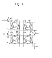
- Figure 1 is a circuit diagram representing a part of a prior semiconductor memory to which the present invention can be applied.
- characters W + and W_ denote a word line pair.
- One end of a first word line W + is connected to a word driver WD.
- the corresponding word line (W + , W_) is changed to the selection state at the "H" (high) level.
- the selected bit line pair (BL, BL) is activated to access the corresponding one of the memory cells MC, located at the cross point between the word line pair and the bit line pair, both of which bit lines (BL, BL) are in a selection state.
- Figure 2A is an enlarged view of two memory cells representative of the memory cells shown in Fig. 1, to explain the problem of double selection
- Figure 2B is a general view of a memory cell arrangement including the two memory cells shown in Fig. 2A.
- Figs. 2A and 2B (and in other figures), members identical to those of Fig. 1 are represented by the same reference characters.
- the memory cell MC1 (T L1 , ...) is in the selection state, and the other cell MC2 (T L2 , ...) is in a half-selection state.
- To be in the selection state means that both the word line and bit line pairs are activated, while the half-selection state means that only the word line pair is activated, i.e., the bit line pair is not activated.
- the above-mentioned double selection is not related to the selection memory cell MC 1 , but to the half-selection memory cell MC 2 .
- the memory cells, except for one selection memory cell MC 1 are all half-selection memory cells MC 2 .
- Character T L2 denotes a load transistor and T ME2 a multi-emitter transistor.
- the multi-emitter transistor T ME2 has a base B 2 , a collector C 2 , a first emitter E21 , and a second emitter E 22 .
- the first emitter E 21 is connected to the first bit line BL, and the second emitter E 22 is connected to the second word line W .
- the second word line W_ is used to carry both the aforesaid hold current I H and the discharge current I D ; the latter is absorbed by a word line discharge current source DS shown in Fig. 2B.
- Figure 3 depicts waveforms of the signals appearing in the memory, to illustrate aspects of the present invention.
- row (a) exhibits changes in the voltage level of the word line W + when the word line changes from the selection state (referred to in the figure as S), to the nonselection state (referred to in the figure as NS), and vice versa.
- the voltage level of the other word line W also changes the same way as that of W + , i.e., corresponding to the changes at W + , but the voltage level at W - is lower than that of W + by a certain level caused by the memory cell MC 2 .
- the change of the state is performed very quickly, particularly during the change from S to NS, due to the presence of the discharge current source DS (Fig.
- the source DS largely absorbs the word line discharge current I D from the word line W - and the I D is then stopped soon after (after the time ⁇ t) the change of the state, by a quick change from on to off state of the discharge current control transistor T D (Fig. 2B).
- the discharge current I D changes along a curve shown in row (b).
- the electric charges stored in the memory cells, and parasitic capacitors along the word line pair with the flow of both currents I H + I D .
- the NPN type transistor T ME2 functions in a reverse mode, i.e. the transistor T ME2 appears to function as a reverse NPN transistor.
- This reverse transistor causes an inverse current i which occurs in all of the half-selected memory cells connected to the selected word line. While the discharge current I is supplied, however, this inverse current i is drawn through the emitter E 22 . Therefore, if the current drawn from the second emitter E22 is stopped (refer to row (b) of Fig. 3), the drawing of inverse current is adversely affected. Since the collector C 2 is the substrate itself, the inverse current flows into and charges the related substrate capacitor CSUB2. Accordingly, the voltage level of the memory cell MC 2 is increased, as a whole, by the thus charged voltage level. The thus increased voltage level creates the aforesaid reoccurrence of the rise Q shown in row (a) of Fig. 3. Under such circumstances, the sudden stop of the word line discharge current I D , as in the curve of row (b) in Fig. 3, remarkably induces such a rise Q.
- the word - line discharge current I D from the second emitter E 22 must not be stopped suddenly, but must be allowed to continue flowing for a while.
- the above-mentioned phrase, "during the inverse operation mode of the multi-emitter transistor” means that period wherein recombinations are performed in the minor carriers that thereafter disappear, which minor carriers have been stored at the base B 2 of the transister T ME2 while it was in the aforesaid saturation state. Usually the minor carriers disappear gradually, almost following the so-called logarithmic attenuation curve.
- the word line discharge current is not stopped suddenly, as depicted in row (b) of Fig. 3, but is progressively reduced according to a predetermined discharging characteristic.
- a discharging characteristic is depicted by the curve of row (c) in Fig. 3, with a word line discharge current I' D .
- Another possibility is to reduce the discharge current linearly, as shown in row (e) of Fig. 3.
- FIG 4 is a general view of a word line discharge current controller CTL in a semiconductor memory embodying the present invention.
- the controller CTL of the arrangement shown is comprised of control circuits CC connected with respective word line pairs.
- Each control circuit CC is operative to draw the word line discharge current which is reduced, during a short time after the change from the selection state to the nonselection state of the corresponding word line, together with a gradual attenuation of the aforesaid inverse current flowing from the corresponding bit line to the corresponding word line W so as to realize any one of the discharging characteristics depicted in rows (b) through (e) of Figure 3.
- Figure 5 is an enlarged cross-sectional view of a part of the memory cell MC 2 shown in Fig. 2A. Principles of an embodiment of the invention as described previously will be explained in more detail, with reference to Fig. 5, to clarify the role of each control circuit CC of Fig. 4.
- the emitter of the load transistor T L2 is connected with the word line W + , the collector is connected with the base of the multi-emitter transistor T ME2 ' and the base is connected with the collector of the transistor T ME2 . All are surrounded by an isolation IS.
- the word line discharge current I is drawn from the second emitter E 22 of the transistor T ME2 to the word line W - . Since the transistor T ME2 is saturated during the selection state, the base-collector junction of the transistor T ME2 is made "on". Therefore, the electric charges ⁇ and ⁇ are stored separately along the border of the base-collector junction, as illustrated.
- the transistor having the emitter E21 is operated in the aforesaid inverse operation mode and the aforesaid inverse current i flows therethrough due to the "H" level of the bit line BL and to the inverse "on” state of the transistor according to the presence of the stored charges ⁇ , ⁇ .
- the inverse current i is proportional to the total of the currents I H + I D .
- the inverse current i can no longer be discharged with the current I D , and accordingly flows into the substrate capacitor C SUB2 , which causes the aforesaid reoccurrence of the rise Q (row (a) in Fig. 3).
- the inverse current i continues to flow until the inverse transistor having the emitter E 22 is turned off.
- the change from "on” to “off” gradually advances almost in line with an advance of the recombinations of the charges ⁇ and ⁇ .
- the inverse current i must be further drawn toward the word line W - until, with the gradually reducing discharge current I D , the stored charges disappear.
- the current I D must be progressively reduced together with a progressive attenuation of the inverse current flowing from the bit line BL to the word line W_.
- the selection memory cell such a gradual reduction of the current I D has no effect, as no inverse current i flows. This is because the selection memory cell is connected with the bit line pair which is at the "L" (low) level.
- FIG. 6 is circuit diagram of the controller CTL of Fig. 4 according to a preferred embodiment of the present invention. 'In Fig. 6, only a first control circuit CC 1 of the controller CTL and a last control circuit CC n are shown, for simplicity, there being n word line pairs. Each control circuit has the same circuit arrangement.
- this control circuit CC 1 is comprised of a dummy cell DC.
- the term "dummy" means a copy of a right (or left) half of the memory cell MC. That is, the dummy cell DC is comprised of a dummy load transistor T L ' and a dummy multi-emitter transistor T ME '.
- the transistor T L ' is connected at its dummy emitter E' to the first word line W + .
- the transistor T' ME is connected at its dummy first emitter E' 1 with a dummy bit line BL' and, at its dummy second emitter E' 2 , with a dummy second word line W_.
- CV denotes a constant voltage source for creating a state equivalent to the state of the selected bit line.
- CS denotes a constant current source for drawing a discharge current, as does the word line discharge current source DS.
- the operations are as follows.
- the voltage level at the dummy emitter E' of the dummy load transistor T' L varies together with the variation in voltage level of the first word line W + .
- the dummy cell DC is active with respect to the constant current source CS. That is, the dummy cell DC is turned on.
- the illustrated word line pair (W + , W - ) is not specified by the input address AD (Fig. 1), the concerned word line pair is changed from the selection state to the nonselection state. During this change, the aforesaid reoccurrence of the rise Q (refer to row (a) of Fig.
- the discharge current control transistor T D is fully biased by the thus increased voltage level V' B , and accordingly, the word line discharge current I D continues to flow through the transistor T D which is still maintained on by the biasing voltage V' B .
- the voltage level V' B varies in accordance with the variation of the rise Q.
- the discharge current I" (row (d) of Fig. 3) is obtained as intended, which current I" has the characteric curve approximated by the previously recited function
- the controller CTL of Fig. 6 produces the following two advantages. First, as mentioned above, the waveform of the current I" D exhibits the same or close to the ideal decreasing curve defined by said N(t), and second, the uniform capability of the gradual reduction of I D is always maintained regardless of differences in the production batch. This is because the dummy cells DC are fabricated by the same process as that of the memory cells MC to be copied.
- LS denotes a level shifter, indicated by chain-dotted lines.
- the level shifter LS assures the current draw of I" via the control transistor TD .
- the transistor T D cannot fully conduct the current I" D where the transistor T operates in a saturation state. Therefore, the transistor T is preferably operated under a nonsaturation state.
- the nonsaturation state can be easily created by reducing the base voltage level V' B by a certain amount.
- the level V' B is determined from the word line (W + ) voltage level with a voltage drop across the dummy cell DC, the level V' B can be lowered by inserting the level shifter between the word line W + and the base of the transistor T D , preferably between the line W + and the dummy emitter E' of the transistor T' L , as illustrated.
- Figure 7A is a circuit diagram of the control circuit CC shown in Fig. 6, including the level shifter LS of Fig. 6 according to a first example.
- the level shifter is composed of a diode D.
- Figure 7B is a circuit diagram of the control circuit CC shown in Fig. 6, including the level shifter LS of Fig. 6 according to a second example.
- the level shifter LS is composed of a resistor R.
- controller CTL of Figures 4 and 6 can reduce the incidence of deleterious double selections occurring between first half-selection memory cells of one word line pair,which changes from the selection state to the nonselection state, and second half-selection memory cells of another word line which changes from the nonselection state to the selection state.
Landscapes
- Engineering & Computer Science (AREA)
- Microelectronics & Electronic Packaging (AREA)
- Computer Hardware Design (AREA)
- Static Random-Access Memory (AREA)
Applications Claiming Priority (2)
| Application Number | Priority Date | Filing Date | Title |
|---|---|---|---|
| JP58053627A JPS59180886A (ja) | 1983-03-31 | 1983-03-31 | ワ−ド線放電回路 |
| JP53627/83 | 1983-03-31 |
Publications (3)
| Publication Number | Publication Date |
|---|---|
| EP0121423A2 true EP0121423A2 (de) | 1984-10-10 |
| EP0121423A3 EP0121423A3 (en) | 1987-04-15 |
| EP0121423B1 EP0121423B1 (de) | 1990-08-16 |
Family
ID=12948142
Family Applications (1)
| Application Number | Title | Priority Date | Filing Date |
|---|---|---|---|
| EP84302182A Expired EP0121423B1 (de) | 1983-03-31 | 1984-03-30 | Wortleitungsentladung in statischen Halbleiterspeichern |
Country Status (4)
| Country | Link |
|---|---|
| US (1) | US4618944A (de) |
| EP (1) | EP0121423B1 (de) |
| JP (1) | JPS59180886A (de) |
| DE (1) | DE3482968D1 (de) |
Families Citing this family (7)
| Publication number | Priority date | Publication date | Assignee | Title |
|---|---|---|---|---|
| US4769785A (en) * | 1986-06-02 | 1988-09-06 | Advanced Micro Devices, Inc. | Writing speed of SCR-based memory cells |
| US5278795A (en) * | 1987-03-27 | 1994-01-11 | U.S. Philips Corporation | Memory circuit having a line decoder with a Darlington-type switching stage and a discharge current source |
| US4858181A (en) * | 1987-07-07 | 1989-08-15 | Texas Instruments Incorporated | Fast recovery PNP loaded bipolar static RAM memory cell with an independent current path |
| CA2042432A1 (en) * | 1990-05-31 | 1991-12-01 | Robert M. Reinschmidt | Memory selection circuit |
| US5117391A (en) * | 1990-06-04 | 1992-05-26 | Motorola, Inc. | Bipolar memory cell array biasing technique with forward active PNP load cell |
| JPH05205483A (ja) * | 1992-01-23 | 1993-08-13 | Sony Corp | バイポーラram回路 |
| KR101986356B1 (ko) * | 2012-10-05 | 2019-06-05 | 삼성전자주식회사 | 반도체 메모리 장치 및 이를 포함하는 장치들 |
Family Cites Families (5)
| Publication number | Priority date | Publication date | Assignee | Title |
|---|---|---|---|---|
| JPS5831673B2 (ja) * | 1979-08-22 | 1983-07-07 | 富士通株式会社 | 半導体記憶装置 |
| JPS5637884A (en) * | 1979-08-30 | 1981-04-11 | Fujitsu Ltd | Terminating circuit for word selective signal line of semiconductor memory unit |
| JPS5831674B2 (ja) * | 1979-12-19 | 1983-07-07 | 株式会社日立製作所 | メモリ |
| JPS6028076B2 (ja) * | 1980-12-25 | 1985-07-02 | 富士通株式会社 | 半導体メモリの書込み回路 |
| US4393476A (en) * | 1981-07-13 | 1983-07-12 | Fairchild Camera & Instrument Corp. | Random access memory dual word line recovery circuitry |
-
1983
- 1983-03-31 JP JP58053627A patent/JPS59180886A/ja active Granted
-
1984
- 1984-03-28 US US06/594,276 patent/US4618944A/en not_active Expired - Fee Related
- 1984-03-30 EP EP84302182A patent/EP0121423B1/de not_active Expired
- 1984-03-30 DE DE8484302182T patent/DE3482968D1/de not_active Expired - Lifetime
Also Published As
| Publication number | Publication date |
|---|---|
| EP0121423A3 (en) | 1987-04-15 |
| EP0121423B1 (de) | 1990-08-16 |
| DE3482968D1 (de) | 1990-09-20 |
| JPH0241111B2 (de) | 1990-09-14 |
| JPS59180886A (ja) | 1984-10-15 |
| US4618944A (en) | 1986-10-21 |
Similar Documents
| Publication | Publication Date | Title |
|---|---|---|
| US4168490A (en) | Addressable word line pull-down circuit | |
| EP0090632B1 (de) | Statische Randomspeicheranordnung | |
| DE3685871T2 (de) | Komplementaere halbleitereinrichtung mit einem substratspannungsgenerator. | |
| KR910003595B1 (ko) | 세그먼트된 워드라인을 갖춘 반도체 메모리 장치 | |
| US4369502A (en) | Semiconductor memory circuit | |
| EP0121423A2 (de) | Wortleitungsentladung in statischen Halbleiterspeichern | |
| EP0025316B1 (de) | Abschlussschaltung für Wortleitungen für eine Halbleiterspeichervorrichtung | |
| US4539661A (en) | Static-type semiconductor memory device | |
| US4459686A (en) | Semiconductor device | |
| EP0053504B1 (de) | Statischer Halbleiterspeicher | |
| US4122548A (en) | Memory storage array with restore circuit | |
| US4651302A (en) | Read only memory including an isolation network connected between the array of memory cells and the output sense amplifier whereby reading speed is enhanced | |
| EP0082695B1 (de) | Halbleiterspeicheranordnung | |
| EP0055409A1 (de) | Halbleiterspeicher | |
| EP0054853A2 (de) | Halbleiterspeicheranordnung | |
| US4821234A (en) | Semiconductor memory device | |
| US4409674A (en) | Semiconductor memory | |
| EP0087919A2 (de) | Statische Halbleiterspeicheranordnung mit einer Wortleitungsentladungsschaltung | |
| US4601014A (en) | Semiconductor memory with word line charge absorbing circuit | |
| US4456979A (en) | Static semiconductor memory device | |
| US4853898A (en) | Bipolar ram having state dependent write current | |
| EP0252780A2 (de) | Speicherzelle mit variabler Klemmschaltung | |
| EP0185156A2 (de) | Direktzugriff-Lese-/Schreibspeicher | |
| EP0107912B1 (de) | Halbleiterspeicheranordnung | |
| JPH0517640B2 (de) |
Legal Events
| Date | Code | Title | Description |
|---|---|---|---|
| PUAI | Public reference made under article 153(3) epc to a published international application that has entered the european phase |
Free format text: ORIGINAL CODE: 0009012 |
|
| AK | Designated contracting states |
Designated state(s): DE FR GB |
|
| PUAL | Search report despatched |
Free format text: ORIGINAL CODE: 0009013 |
|
| AK | Designated contracting states |
Kind code of ref document: A3 Designated state(s): DE FR GB |
|
| 17P | Request for examination filed |
Effective date: 19870825 |
|
| 17Q | First examination report despatched |
Effective date: 19880419 |
|
| GRAA | (expected) grant |
Free format text: ORIGINAL CODE: 0009210 |
|
| AK | Designated contracting states |
Kind code of ref document: B1 Designated state(s): DE FR GB |
|
| REF | Corresponds to: |
Ref document number: 3482968 Country of ref document: DE Date of ref document: 19900920 |
|
| PGFP | Annual fee paid to national office [announced via postgrant information from national office to epo] |
Ref country code: FR Payment date: 19901023 Year of fee payment: 8 |
|
| ET | Fr: translation filed | ||
| PGFP | Annual fee paid to national office [announced via postgrant information from national office to epo] |
Ref country code: GB Payment date: 19910319 Year of fee payment: 8 |
|
| PGFP | Annual fee paid to national office [announced via postgrant information from national office to epo] |
Ref country code: DE Payment date: 19910522 Year of fee payment: 8 |
|
| PLBE | No opposition filed within time limit |
Free format text: ORIGINAL CODE: 0009261 |
|
| STAA | Information on the status of an ep patent application or granted ep patent |
Free format text: STATUS: NO OPPOSITION FILED WITHIN TIME LIMIT |
|
| 26N | No opposition filed | ||
| PG25 | Lapsed in a contracting state [announced via postgrant information from national office to epo] |
Ref country code: GB Effective date: 19920330 |
|
| GBPC | Gb: european patent ceased through non-payment of renewal fee | ||
| PG25 | Lapsed in a contracting state [announced via postgrant information from national office to epo] |
Ref country code: FR Effective date: 19921130 |
|
| PG25 | Lapsed in a contracting state [announced via postgrant information from national office to epo] |
Ref country code: DE Effective date: 19921201 |
|
| REG | Reference to a national code |
Ref country code: FR Ref legal event code: ST |