EP0121700A2 - Appareil de sérialisation de mémoire pour ordinateur de multitraitement - Google Patents
Appareil de sérialisation de mémoire pour ordinateur de multitraitement Download PDFInfo
- Publication number
- EP0121700A2 EP0121700A2 EP84101734A EP84101734A EP0121700A2 EP 0121700 A2 EP0121700 A2 EP 0121700A2 EP 84101734 A EP84101734 A EP 84101734A EP 84101734 A EP84101734 A EP 84101734A EP 0121700 A2 EP0121700 A2 EP 0121700A2
- Authority
- EP
- European Patent Office
- Prior art keywords
- storage
- register
- processor
- page
- page address
- Prior art date
- Legal status (The legal status is an assumption and is not a legal conclusion. Google has not performed a legal analysis and makes no representation as to the accuracy of the status listed.)
- Granted
Links
Images

Classifications
-
- G—PHYSICS
- G06—COMPUTING OR CALCULATING; COUNTING
- G06F—ELECTRIC DIGITAL DATA PROCESSING
- G06F9/00—Arrangements for program control, e.g. control units
- G06F9/06—Arrangements for program control, e.g. control units using stored programs, i.e. using an internal store of processing equipment to receive or retain programs
- G06F9/46—Multiprogramming arrangements
- G06F9/52—Program synchronisation; Mutual exclusion, e.g. by means of semaphores
Definitions
- This invention relates to multiprocessor computer systems and more particularly to storage serialization apparatus for enabling the multiprocessors to concurrently execute instructions.
- the invention finds particular utility in a tightly coupled multiprocessor computer system having virtual storage.
- a storage access serialization mechanism operates in a manner where if two or more processors are attempting to update the same storage location, the modification by one processor is not lost by simultaneous modification by another processor.
- One processor is allowed to complete its storage access of the storage location being simultaneously accessed and all other processors are locked out from accessing that location until the granted access is complete.
- Prior art which protects storage locations from unauthorized access is represented by U. S. - A - 3, 264,515 .
- the present invention does not provide for or preclude a protected area of storage. There is no provision to prevent an instruction stream from accessing unauthorized data.
- the present invention provides a serialization function whereby when one or more processors are attempting to access the same storage location at the same time, one processor is locked out until the other completes its access.
- the principal objects of the invention are to provide storage serialization apparatus in a multiprocessor computer system which (a) locks only a portion of storage and (b) locks a portion of storage only for one instruction execution time.
- each instruction imposes a lock on storage pages containing the operands of the instruction and allowing other processors to execute instructions without any delays unless an instruction being executed by one processor requires access to a page locked by an instruction of another processor. At the end of an instruction; the page or pages being locked by that instruction are unlocked.
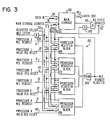
- FIG. 1 With reference to the drawings and particularly to Fig. 1, the invention is shown by way of example as being incorporated into a multi-processor computer system which can be of the type shown and described in Fig. 1, processors 10, 20, 30 and 40 can concurrently execute instructions which access storage 100 via storage control 50.
- processors 10, 20, 30 and 40 can concurrently execute instructions which access storage 100 via storage control 50.
- the input/output devices and channels associated with each of the processors are not shown but are considered as being included with the processors.
- Main storage 100 in this particular example, is addressed virtually by the processors and each processor includes a virtual address translator which translates the virtual address into a real main storage address.
- Main storage 100 consists of a predetermined number of page frames, which in this example correspond in size to a 512 byte page of the virtual storage. Virtual storage and virtual addressing concepts are well known in the art.
- Any byte of data in a program in process in the processors has two addresses, i.e., a virtual address and a real address.
- a virtual address i.e., a virtual address
- a real address any page or 512 byte block can be paged out of main storage 100 to auxiliary storage in the processor and subsequently paged into a new main storage location any number of times before the processing of the program is completed.
- the virtual address of a byte of data remains unchanged, the real main storage address can change many times during the processing or execution of the program.
- Each main storage request made by the processors is intercepted by associative register stack 150.
- the addresses of the pages or pieces of storage being used by each of the processors 10, 20, 30 and 40 are held in the associative register stack 150 whereby a record is maintained of the pages each processor has exclusive use.
- the duration of serialization is for one instruction execution time. Instruction fetch does not require serialization of main storage 100 because a processor is reading and not writing. Only instruction operands need be serialized. In this example, an instruction can have two operands and either operand can be up to 256 bytes in length. Thus either operand can occupy part of two pages. Consequently the associative register stack for each processor includes four registers and are represented by register blocks 160, 170, 180 and -190 to correspond with processors 10, 20, 30 and 40 respectively, Fig. 3.
- a deadlock can occur between two of the processors 10, 20, 30 or 40, because both can request exclusive- use of the same page of storage, the logic for arbitrating and breaking possible deadlocks is represented in Fig. 2. If a deadlock occurs between two of the processors, the storage request command will be rejected X number of times. The processor will then release the locks already held by removing the entries in the associative register array and then restarts the instruction. Each of the processors 10, 20, 30 and 40 can be given a different value X depending upon its processor ID and this will prevent a repeat of the deadlock.
- operand 1 of the instruction is fetched and an entry is made in the related register array of the register arrays 160, 170, 180 and 190. If a page crossing is detected while fetching operand 1, an entry is made into the operand 1 page crossing register in the register block. Operand 2 is then fetched and an entry is made in the associative register array. If operand 2 crosses a page, then an entry is made in the operand 2 page crossing register of the associative register array block. Only when all operands are successfully locked by entries in the associative register array block for that particular processor, then execution of the instruction proceeds. In Fig.
- Fig. 3 data is entered into main storage 100 over Data In bus 55 from storage control 50, Fig. 1 and data is read from main storage 100 to one of the processors via storage control 50 over bus 60.
- the main storage addresses are applied to main storage 100 from storage control 50 via main storage address bus 70.
- the page portion of the main storage address is also applied via bus 71 to processor register blocks 160, 170, 180 and 190, Fig. 3.
- the processor When an instruction address is passed by one of the processors onto the main storage address bus 70, the processor also activates an associated main storage request line such as lines 11, 21, 31 and 41 for processors 10, 20, 30 and 40 respectively.
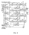
- the processor register blocks 160, 170, 180 and 190 are identical and the details of block 160 are shown in Fig. 4.
- the processor register block 160 contains four registers 201, 203, 205 and 207, two of the registers being for operand 1 and two for operand 2.
- the register blocks 160, 170, 180 and 190 function in a manner where the register block associated with the processor making the storage access request forces a non-address match by inhibiting the AND circuits, in the case of block 160, AND circuits 226, 227, 228 and 229, which are fed by comparators 210, 211, 212 and 213 respectively.
- Comparators 210, 211, 212 and 213 compare the page addresses in registers 201, 203, 205 and 207 with the page address on bus 71.
- the writing of the page address into the selected register is controlled by two groups of AND circuits, Fig. 4.
- the page address is applied to AND circuits 221, 222, 223 and 224 which are representative of AND circuits for the bits of the page address.
- AND circuits have their outputs connected to registers 201, 203, 205 and 207 respectively and are conditioned by outputs of AND circuits 216, 217, 218 and 219 respectively.
- Register selection is accomplished via the AND circuits 216, 217, 218 and 219 which are representative of AND circuits having inputs from register select bus 215.
- These AND circuits are inhibited by the instruction fetch INST FETCH signal via inverter 220 and are conditioned by the M.S. Cycle Granted signal from AND circuit 105, Fig. 3, on line 110.
- the Processor M.S. Request signal also must be present for these AND circuits to have an output. Hence, the page address is only written into the selected register in the absence of an instruction fetch of the register block associated with the processor making the main storage access request.
- Valid Register latches 202, 204, 206 and 208 When a page address is entered into the selected register an associated valid register latch of Valid Register latches 202, 204, 206 and 208 is set. The set outputs of these latches are applied to inputs of AND circuits 226, 227, 228 and 229 respectively.
- the Valid Register latches are essentially the storage access locks and must be reset by a processor at the end of instruction execution cycle. This is accomplished by the processors 10, 20, 30 or 40 activating their Processor Valid REG RST signals on lines 12, 22, 32 and 42 respectively.
- the operation of the associative register stack 150, Figs. 1, 3 and 4 will be described with an instruction execution sequence.
- An instruction address is passed by one of the processors 10, 20, 30 or 40 via storage control 50 to main storage 100 over the main storage address bus 70.
- the Valid Register latches in the processor register blocks 160, 170, 180 and 190 are initially all reset and thus the output from OR circuit 230 in the case of register block 160 and similar OR circuits for register blocks 170, 180 and 190 and thus the output of OR circuit 240, Fig. 3, will be inactive or at a level whereby inverter 245 conditions AND circuit 105 which then passes a M.S. Cycle Granted signal on line 110.
- the processor presenting the main storage address on bus 70 also provides a main storage request signal, for processor 10 for example, on line 11.
- a comparison is made between the contents of the registers of the register blocks with the main storage page address on bus 71 to determine if the page portion of the address is contained in any of these registers. With all of the Valid Register latches in a register block reset, there will be no comparison and the main storage cycle will be granted.
- the instruction fetched from main storage 100 is sent to the requesting processor via the data bus out 60 along with the indication from AND circuit 105 indicating that the main storage cycle was granted. Because an instruction is being fetched from storage no entry is made into the registers of the register block associated with the processor making the main storage request.
- the processor which received the instruction starts the execution of that instruction by initiating an operand fetch.
- the address of the operand is placed on the main storage address bus 70 and the appropriate main storage request line is made active.
- the address for one of the registers into which the page address is to be written is placed on the register select bus 215.
- An address comparison is made in the register blocks for all processors and assuming no matches, the operand 1 data is sent to the processor executing the instruction via data out bus 60 together with the signal from AND circuit 105 indicating that a main storage cycle is granted. This time, however, the address of operand 1 is entered into the register associated with that operand. Additionally, the associated valid register latch is set.
- the processor executing the instruction then continues with fetching the second portion of operand 1 if operand 1 crosses a page boundary or fetches operand 2.
- the address for fetching the second part of operand 1 or for fetching operand 2 will not compare with the address stored in the register associated with the first part of operand 1. For each of the operand fetches, the page portion of the address is placed in the appropriate registers of the register block.
- the comparators 210, 211, 212 and 213 will indicate address matches however theses match indications will be nullified by inverter 231 because the addresses are valid for use by processor 10 but are not valid for use by processors 20, 30 and 40.
- a non-compare is forced in the processor register block for the processor requesting a main storage access but the comparisons in the other processor register blocks 170, 180 and 190 are tested because there will be an absence of a main storage request signal on the main storage request lines 21, 31 and 41.
- the main storage cycle is granted to the processor making the main storage request. This main storage cycle granted signal is then used to load the main storage address into one of the registers of the processor register block associated with the processor requesting the main storage access and in this instance processor register block 160 provided the main storage request which was not for an instruction fetch.
- the AND circuits 216, 217, 218 and 219 for processor register block 160 are conditioned by the main storage request signal on line 11 and at this time are not inhibited by the instruction fetch signal via inverter 220.
- One of the AND circuits 216, 217, 218 or 219 will be conditioned and selected based upon the selection made via the register select bus 215 whereby one of the AND circuits 216, 217, 218 or 219 passes a signal to condition the associated AND circuit of AND circuits 221, 222, 223 and 224 and sets the associated Valid Register latch of the valid register latches 202, 204, 206 and 208.
- the register associated with the conditioned AND circuit will receive the page address of the main storage address and with the associated valid register latch set, any subsequent comparison will be tested unless that comparison is in the processor register block for the processor making the main storage request. However, if during execution of the instruction by processor 10 one of the other processors 20, 30 or 40 made a main storage request using an address which was the same as the address stored in one of the registers 201, 203, 205 or 207 then there would be a comparison and the AND circuit of the AND circuits 226, 227, 228 or 229 associated with the set valid register latch would pass a signal indicating an address match and this signal would be passed by OR circuit 240 of Fig. 3 indicating a main storage request rejected condition.
- the ti.S. Request Rejected signal would only be generated if processor 10, in this instance, was not finished with the execution of the instruction it had been executing.
- processor 10 finishes with the instruction it had been executing, it presents a Valid Register Reset signal on line 12 for resetting all of the previously set valid register latches 202, 204, 206 and 208.
- a Valid Register Reset signal on line 12 for resetting all of the previously set valid register latches 202, 204, 206 and 208.
- processor 10 had been accessing a location in a page of storage other than one which had been accessed by processor 10 then its storage access would have been granted.
Landscapes
- Engineering & Computer Science (AREA)
- Software Systems (AREA)
- Theoretical Computer Science (AREA)
- Physics & Mathematics (AREA)
- General Engineering & Computer Science (AREA)
- General Physics & Mathematics (AREA)
- Memory System Of A Hierarchy Structure (AREA)
- Multi Processors (AREA)
- Memory System (AREA)
Applications Claiming Priority (2)
| Application Number | Priority Date | Filing Date | Title |
|---|---|---|---|
| US06/479,281 US4891749A (en) | 1983-03-28 | 1983-03-28 | Multiprocessor storage serialization apparatus |
| US479281 | 1983-03-28 |
Publications (3)
| Publication Number | Publication Date |
|---|---|
| EP0121700A2 true EP0121700A2 (fr) | 1984-10-17 |
| EP0121700A3 EP0121700A3 (en) | 1987-11-19 |
| EP0121700B1 EP0121700B1 (fr) | 1989-10-11 |
Family
ID=23903349
Family Applications (1)
| Application Number | Title | Priority Date | Filing Date |
|---|---|---|---|
| EP84101734A Expired EP0121700B1 (fr) | 1983-03-28 | 1984-02-20 | Appareil de sérialisation de mémoire pour ordinateur de multitraitement |
Country Status (4)
| Country | Link |
|---|---|
| US (1) | US4891749A (fr) |
| EP (1) | EP0121700B1 (fr) |
| JP (1) | JPS59180767A (fr) |
| DE (1) | DE3480129D1 (fr) |
Cited By (10)
| Publication number | Priority date | Publication date | Assignee | Title |
|---|---|---|---|---|
| WO1988008569A1 (fr) * | 1987-05-01 | 1988-11-03 | Digital Equipment Corporation | Procede et appareil de gestion d'indicateurs de verrouillage multiple dans un systeme ordinateur a multiprocesseur |
| GB2218832A (en) * | 1988-05-16 | 1989-11-22 | Ardent Computer Corp | Instruction chaining and data hazard resolution system |
| US4941083A (en) * | 1987-05-01 | 1990-07-10 | Digital Equipment Corporation | Method and apparatus for initiating interlock read transactions on a multiprocessor computer system |
| US4949239A (en) * | 1987-05-01 | 1990-08-14 | Digital Equipment Corporation | System for implementing multiple lock indicators on synchronous pended bus in multiprocessor computer system |
| US4969117A (en) * | 1988-05-16 | 1990-11-06 | Ardent Computer Corporation | Chaining and hazard apparatus and method |
| EP0438021A3 (en) * | 1990-01-17 | 1991-12-04 | International Business Machines Corporation | Synchronization instruction for multiple processor network |
| EP0297895A3 (fr) * | 1987-07-01 | 1992-01-22 | Digital Equipment Corporation | Dispositif et méthode utilisant exclusion pour synchroniser l'accès à des groupes de signaux de la mémoire principale dans un système multiprocesseur de traitement des données |
| US5291581A (en) * | 1987-07-01 | 1994-03-01 | Digital Equipment Corporation | Apparatus and method for synchronization of access to main memory signal groups in a multiprocessor data processing system |
| US5341510A (en) * | 1987-05-01 | 1994-08-23 | Digital Equipment Corporation | Commander node method and apparatus for assuring adequate access to system resources in a multiprocessor |
| EP0911731A3 (fr) * | 1997-10-24 | 2000-08-09 | Compaq Computer Corporation | Mécanisme pour le sequencement dans un système multiprocesseur basé sur commutateurs |
Families Citing this family (18)
| Publication number | Priority date | Publication date | Assignee | Title |
|---|---|---|---|---|
| US5142676A (en) * | 1988-12-28 | 1992-08-25 | Gte Laboratories Incorporated | Separate content addressable memories for storing locked segment addresses and locking processor identifications for controlling access to shared memory |
| US5226159A (en) * | 1989-05-15 | 1993-07-06 | International Business Machines Corporation | File lock management in a distributed data processing system |
| EP0432075B1 (fr) * | 1989-11-09 | 1997-02-26 | International Business Machines Corporation | Multiprocesseur à instructions relativement atomiques |
| US5287473A (en) * | 1990-12-14 | 1994-02-15 | International Business Machines Corporation | Non-blocking serialization for removing data from a shared cache |
| US5276835A (en) * | 1990-12-14 | 1994-01-04 | International Business Machines Corporation | Non-blocking serialization for caching data in a shared cache |
| EP0513519A1 (fr) * | 1991-05-15 | 1992-11-19 | International Business Machines Corporation | Système de mémoire pour systèmes multiprocesseurs |
| JP2781092B2 (ja) * | 1991-11-06 | 1998-07-30 | 富士通株式会社 | システム間排他制御方式 |
| JPH05210640A (ja) * | 1992-01-31 | 1993-08-20 | Hitachi Ltd | マルチプロセッサシステム |
| US5388266A (en) * | 1992-03-30 | 1995-02-07 | International Business Machines Corporation | Management of data objects used intain state information for shared data at a local complex |
| US5274823A (en) * | 1992-03-31 | 1993-12-28 | International Business Machines Corporation | Interrupt handling serialization for process level programming |
| JP2675961B2 (ja) * | 1992-05-20 | 1997-11-12 | インターナショナル・ビジネス・マシーンズ・コーポレイション | 実記憶のページをロックするための方法 |
| US5727155A (en) * | 1994-09-09 | 1998-03-10 | Intel Corporation | Method and apparatus for dynamically controlling a remote system's access to shared applications on a host system |
| US5719890A (en) * | 1995-06-01 | 1998-02-17 | Micron Technology, Inc. | Method and circuit for transferring data with dynamic parity generation and checking scheme in multi-port DRAM |
| US6487207B1 (en) | 1997-02-26 | 2002-11-26 | Micron Technology, Inc. | Shared buffer memory architecture for asynchronous transfer mode switching and multiplexing technology |
| US6088791A (en) * | 1998-04-30 | 2000-07-11 | International Business Machines Corporation | Computer processor system for implementing the ESA/390 STOSM and STNSM instructions without serialization or artificially extending processor execution time |
| US6088792A (en) * | 1998-04-30 | 2000-07-11 | International Business Machines Corporation | Avoiding processor serialization after an S/390 SPKA instruction |
| US7953932B2 (en) * | 2008-02-13 | 2011-05-31 | International Business Machines Corporation | System and method for avoiding deadlocks when performing storage updates in a multi-processor environment |
| US9160607B1 (en) * | 2012-11-09 | 2015-10-13 | Cray Inc. | Method and apparatus for deadlock avoidance |
Family Cites Families (12)
| Publication number | Priority date | Publication date | Assignee | Title |
|---|---|---|---|---|
| US3469239A (en) * | 1965-12-02 | 1969-09-23 | Hughes Aircraft Co | Interlocking means for a multi-processor system |
| US4318182A (en) * | 1974-04-19 | 1982-03-02 | Honeywell Information Systems Inc. | Deadlock detection and prevention mechanism for a computer system |
| US4104718A (en) * | 1974-12-16 | 1978-08-01 | Compagnie Honeywell Bull (Societe Anonyme) | System for protecting shared files in a multiprogrammed computer |
| JPS5813932B2 (ja) * | 1975-04-07 | 1983-03-16 | 株式会社日立製作所 | 記憶装置の多重使用制御方式 |
| JPS526032A (en) * | 1975-07-04 | 1977-01-18 | Hitachi Ltd | Main storage control unit |
| US4037215A (en) * | 1976-04-30 | 1977-07-19 | International Business Machines Corporation | Key controlled address relocation translation system |
| US4099243A (en) * | 1977-01-18 | 1978-07-04 | Honeywell Information Systems Inc. | Memory block protection apparatus |
| US4325116A (en) * | 1979-08-21 | 1982-04-13 | International Business Machines Corporation | Parallel storage access by multiprocessors |
| GB2059652B (en) * | 1979-09-29 | 1983-08-24 | Plessey Co Ltd | Memory protection system using capability registers |
| US4415972A (en) * | 1980-12-29 | 1983-11-15 | Sperry Corporation | Dual port memory interlock |
| US4435766A (en) * | 1981-06-16 | 1984-03-06 | International Business Machines Corporation | Nested resource control using locking and unlocking routines with use counter for plural processes |
| US4445197A (en) * | 1981-10-27 | 1984-04-24 | International Business Machines Corporation | Weak synchronization and scheduling among concurrent asynchronous processors |
-
1983
- 1983-03-28 US US06/479,281 patent/US4891749A/en not_active Expired - Fee Related
-
1984
- 1984-02-03 JP JP59017261A patent/JPS59180767A/ja active Pending
- 1984-02-20 EP EP84101734A patent/EP0121700B1/fr not_active Expired
- 1984-02-20 DE DE8484101734T patent/DE3480129D1/de not_active Expired
Non-Patent Citations (3)
| Title |
|---|
| IBM TECHNICAL DISCLOSURE BULLETIN, vol. 14, no. 5, October 1971, pages 1543-1544, New York, US; A.W. BIDWELL et al.: "Shared storage locking facility" * |
| IBM TECHNICAL DISCLOSURE BULLETIN, vol. 23, no. 5, October 1980, pages 1801-1804, New York, US; R.E. BIRNEY et al.: "Shared storage for multiple processors" * |
| IBM TECHNICAL DISCLOSURE BULLETIN, vol. 24, no. 3, August 1981, pages 1586-1587, New York, US; B.C. GOLDSTEIN et al.: "Page and segment locking schema" * |
Cited By (12)
| Publication number | Priority date | Publication date | Assignee | Title |
|---|---|---|---|---|
| WO1988008569A1 (fr) * | 1987-05-01 | 1988-11-03 | Digital Equipment Corporation | Procede et appareil de gestion d'indicateurs de verrouillage multiple dans un systeme ordinateur a multiprocesseur |
| US4858116A (en) * | 1987-05-01 | 1989-08-15 | Digital Equipment Corporation | Method and apparatus for managing multiple lock indicators in a multiprocessor computer system |
| US4941083A (en) * | 1987-05-01 | 1990-07-10 | Digital Equipment Corporation | Method and apparatus for initiating interlock read transactions on a multiprocessor computer system |
| US4949239A (en) * | 1987-05-01 | 1990-08-14 | Digital Equipment Corporation | System for implementing multiple lock indicators on synchronous pended bus in multiprocessor computer system |
| US5341510A (en) * | 1987-05-01 | 1994-08-23 | Digital Equipment Corporation | Commander node method and apparatus for assuring adequate access to system resources in a multiprocessor |
| EP0297895A3 (fr) * | 1987-07-01 | 1992-01-22 | Digital Equipment Corporation | Dispositif et méthode utilisant exclusion pour synchroniser l'accès à des groupes de signaux de la mémoire principale dans un système multiprocesseur de traitement des données |
| US5291581A (en) * | 1987-07-01 | 1994-03-01 | Digital Equipment Corporation | Apparatus and method for synchronization of access to main memory signal groups in a multiprocessor data processing system |
| GB2218832A (en) * | 1988-05-16 | 1989-11-22 | Ardent Computer Corp | Instruction chaining and data hazard resolution system |
| US4969117A (en) * | 1988-05-16 | 1990-11-06 | Ardent Computer Corporation | Chaining and hazard apparatus and method |
| GB2218832B (en) * | 1988-05-16 | 1992-08-26 | Ardent Computer Corp | Chaining and hazard apparatus and method |
| EP0438021A3 (en) * | 1990-01-17 | 1991-12-04 | International Business Machines Corporation | Synchronization instruction for multiple processor network |
| EP0911731A3 (fr) * | 1997-10-24 | 2000-08-09 | Compaq Computer Corporation | Mécanisme pour le sequencement dans un système multiprocesseur basé sur commutateurs |
Also Published As
| Publication number | Publication date |
|---|---|
| JPS59180767A (ja) | 1984-10-13 |
| EP0121700A3 (en) | 1987-11-19 |
| EP0121700B1 (fr) | 1989-10-11 |
| US4891749A (en) | 1990-01-02 |
| DE3480129D1 (en) | 1989-11-16 |
Similar Documents
| Publication | Publication Date | Title |
|---|---|---|
| EP0121700B1 (fr) | Appareil de sérialisation de mémoire pour ordinateur de multitraitement | |
| US5185871A (en) | Coordination of out-of-sequence fetching between multiple processors using re-execution of instructions | |
| US5761734A (en) | Token-based serialisation of instructions in a multiprocessor system | |
| US5276848A (en) | Shared two level cache including apparatus for maintaining storage consistency | |
| US5202972A (en) | Store buffer apparatus in a multiprocessor system | |
| EP0690371B1 (fr) | Tampon d'extraction et stockage de données pour l'exécution hors-séquence dans un système de traitement de données | |
| US4991090A (en) | Posting out-of-sequence fetches | |
| US4504902A (en) | Cache arrangement for direct memory access block transfer | |
| US5291586A (en) | Hardware implementation of complex data transfer instructions | |
| US4408274A (en) | Memory protection system using capability registers | |
| US5257354A (en) | System for monitoring and undoing execution of instructions beyond a serialization point upon occurrence of in-correct results | |
| US4851991A (en) | Central processor unit for digital data processing system including write buffer management mechanism | |
| EP0303648B1 (fr) | Unite centrale pour systeme informatique numerique comprenant un mecanisme de gestion d'antememoire | |
| GB1586847A (en) | Data processing apparatus | |
| US6148394A (en) | Apparatus and method for tracking out of order load instructions to avoid data coherency violations in a processor | |
| US4930106A (en) | Dual cache RAM for rapid invalidation | |
| US5119484A (en) | Selections between alternate control word and current instruction generated control word for alu in respond to alu output and current instruction | |
| US5339397A (en) | Hardware primary directory lock | |
| US6745274B1 (en) | Apparatus and method for synchronizing multiple accesses to common resources | |
| US4970643A (en) | Mechanism for lock-up free cache operation with a remote address translation unit | |
| US6138206A (en) | Data register for multicycle data cache read | |
| EP0187713B1 (fr) | Mémoire de système pour processeur de réduction exécutant des programmes mémorisés en graphes binaires employant des codes de langage appliqués sans variable | |
| US5276892A (en) | Destination control logic for arithmetic and logic unit for digital data processor | |
| JPH055137B2 (fr) | ||
| EP0375892B1 (fr) | Système de traitement de données |
Legal Events
| Date | Code | Title | Description |
|---|---|---|---|
| PUAI | Public reference made under article 153(3) epc to a published international application that has entered the european phase |
Free format text: ORIGINAL CODE: 0009012 |
|
| AK | Designated contracting states |
Designated state(s): DE FR GB |
|
| 17P | Request for examination filed |
Effective date: 19841123 |
|
| PUAL | Search report despatched |
Free format text: ORIGINAL CODE: 0009013 |
|
| AK | Designated contracting states |
Kind code of ref document: A3 Designated state(s): DE FR GB |
|
| 17Q | First examination report despatched |
Effective date: 19880205 |
|
| GRAA | (expected) grant |
Free format text: ORIGINAL CODE: 0009210 |
|
| AK | Designated contracting states |
Kind code of ref document: B1 Designated state(s): DE FR GB |
|
| REF | Corresponds to: |
Ref document number: 3480129 Country of ref document: DE Date of ref document: 19891116 |
|
| ET | Fr: translation filed | ||
| PLBE | No opposition filed within time limit |
Free format text: ORIGINAL CODE: 0009261 |
|
| STAA | Information on the status of an ep patent application or granted ep patent |
Free format text: STATUS: NO OPPOSITION FILED WITHIN TIME LIMIT |
|
| 26N | No opposition filed | ||
| PGFP | Annual fee paid to national office [announced via postgrant information from national office to epo] |
Ref country code: GB Payment date: 19920113 Year of fee payment: 9 |
|
| PGFP | Annual fee paid to national office [announced via postgrant information from national office to epo] |
Ref country code: FR Payment date: 19920124 Year of fee payment: 9 |
|
| PGFP | Annual fee paid to national office [announced via postgrant information from national office to epo] |
Ref country code: DE Payment date: 19920304 Year of fee payment: 9 |
|
| PG25 | Lapsed in a contracting state [announced via postgrant information from national office to epo] |
Ref country code: GB Effective date: 19930220 |
|
| GBPC | Gb: european patent ceased through non-payment of renewal fee |
Effective date: 19930220 |
|
| PG25 | Lapsed in a contracting state [announced via postgrant information from national office to epo] |
Ref country code: FR Effective date: 19931029 |
|
| PG25 | Lapsed in a contracting state [announced via postgrant information from national office to epo] |
Ref country code: DE Effective date: 19931103 |
|
| REG | Reference to a national code |
Ref country code: FR Ref legal event code: ST |