EP0121703B1 - A method and a circuit for processing pulses of a pulse train - Google Patents
A method and a circuit for processing pulses of a pulse train Download PDFInfo
- Publication number
- EP0121703B1 EP0121703B1 EP84101760A EP84101760A EP0121703B1 EP 0121703 B1 EP0121703 B1 EP 0121703B1 EP 84101760 A EP84101760 A EP 84101760A EP 84101760 A EP84101760 A EP 84101760A EP 0121703 B1 EP0121703 B1 EP 0121703B1
- Authority
- EP
- European Patent Office
- Prior art keywords
- pulse
- signal
- pulses
- channel
- processed
- Prior art date
- Legal status (The legal status is an assumption and is not a legal conclusion. Google has not performed a legal analysis and makes no representation as to the accuracy of the status listed.)
- Expired
Links
- 238000000034 method Methods 0.000 title claims description 25
- 238000012545 processing Methods 0.000 title claims description 24
- 238000001514 detection method Methods 0.000 claims description 7
- 230000003111 delayed effect Effects 0.000 claims description 4
- 230000002285 radioactive effect Effects 0.000 claims description 4
- 238000013213 extrapolation Methods 0.000 claims 1
- 230000008030 elimination Effects 0.000 description 39
- 238000003379 elimination reaction Methods 0.000 description 39
- 230000010354 integration Effects 0.000 description 21
- 239000003990 capacitor Substances 0.000 description 15
- 238000012937 correction Methods 0.000 description 12
- 238000007599 discharging Methods 0.000 description 12
- 238000013461 design Methods 0.000 description 7
- 238000010586 diagram Methods 0.000 description 6
- 239000013078 crystal Substances 0.000 description 5
- 239000011159 matrix material Substances 0.000 description 4
- 230000005855 radiation Effects 0.000 description 4
- 241000452277 Callicore texa Species 0.000 description 3
- 238000012986 modification Methods 0.000 description 3
- 230000004048 modification Effects 0.000 description 3
- 101150095095 TIMELESS gene Proteins 0.000 description 2
- 230000004069 differentiation Effects 0.000 description 2
- 230000006870 function Effects 0.000 description 2
- 210000000056 organ Anatomy 0.000 description 2
- 239000004065 semiconductor Substances 0.000 description 2
- 230000008878 coupling Effects 0.000 description 1
- 238000010168 coupling process Methods 0.000 description 1
- 238000005859 coupling reaction Methods 0.000 description 1
- 238000003745 diagnosis Methods 0.000 description 1
- 230000009977 dual effect Effects 0.000 description 1
- 230000000694 effects Effects 0.000 description 1
- 230000005251 gamma ray Effects 0.000 description 1
- 230000001771 impaired effect Effects 0.000 description 1
- 230000002452 interceptive effect Effects 0.000 description 1
- 238000011835 investigation Methods 0.000 description 1
- 238000003672 processing method Methods 0.000 description 1
- 230000000717 retained effect Effects 0.000 description 1
- 239000000126 substance Substances 0.000 description 1
- 235000019640 taste Nutrition 0.000 description 1
- 230000001960 triggered effect Effects 0.000 description 1
Images


Classifications
-
- G—PHYSICS
- G01—MEASURING; TESTING
- G01T—MEASUREMENT OF NUCLEAR OR X-RADIATION
- G01T1/00—Measuring X-radiation, gamma radiation, corpuscular radiation, or cosmic radiation
- G01T1/16—Measuring radiation intensity
- G01T1/17—Circuit arrangements not adapted to a particular type of detector
Definitions
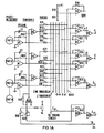
- the +Y, -Y output signals are fed to a differential amplifier A9 where the +Y and -Y signals are consolidated into a single event Y positional coordinate signal.
- the differential amplifier A10 developes a single consolidated X positional coordinate signal.
- the Z t signal passes through the amplifier A11.
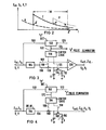
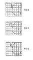
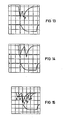
- FIG. 2 shows in a schematic pulse diagram a typical pulse configuration which can possibly occur in a Z nt , Z,, X and Y signal as described previously and which has to be processed according to the invention.
- the dashed line is the tail of a "A" pulse that precedes a potentially valid true pulse "T” shown as a solid line.
- a piling up or "P" pulse shown in dotted line may arrive while the integration time window IW of an integrator circuitry 24, 26, 28 and 30 is open and thus impairs proper integration of the valid true pulse "T".
- the "T" pulse detector circuitry 102 can be reset at the end of integration time (normally about 900 ns).
- the second channel is connected with the inverting input of a differential amplifier 128.
- the third channel is connected with the non inverting input of said differential amplifier 128.
- This discharging signal of said capacitor C of said RC circuit 112, which simulates the tail of an "A" pulse is then superimposed with the signal in said third channel by the differential amplifier 128 such that the discharge signal in the second channel 106 is subtracted from the signal in the third channel 108.
- the signal in the third channel 108 is the "T” pulse puled up on the tail of the "A” pulse, as shown in Fig. 2, due to the subtraction a "A" pulse eliminated signal (Z ntE' Z tE , X E or Y E ) is produced at the output of the differential amplifier 128 i.e. a potentially valid true "T" pulse.
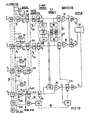
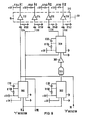
- the switch logic circuitry 206 is controlled by the "T" pulse detector circuitry 190 via line 216 and it is also controlled by the "P" pulse detector circuitry via line 218. Via line 220 an integration period IW of an integrator circuitry is started at the occurrence of a "T" pulse. Via line 222 the "T" pulse detector circuitry 190 and via line 224 the “P” pulse detector circuitry 192 is reset at the end of an integration period IW.
- the output of the second channel 186 is again connected to the inverting input of a differential amplifier 226 and the output of the fourth channel 188 is connected to the non inverting input of the differential amplifier 226.
- the "T” pulse detector circuitry 190 and the "P” pulse detector circuitry 192 are again leading edge detectors (both Signetics NE 521 for example) as described before with regard to the circuits of Figures 3 and 4.
Landscapes
- Physics & Mathematics (AREA)
- Health & Medical Sciences (AREA)
- Life Sciences & Earth Sciences (AREA)
- General Physics & Mathematics (AREA)
- High Energy & Nuclear Physics (AREA)
- Molecular Biology (AREA)
- Spectroscopy & Molecular Physics (AREA)
- Measurement Of Radiation (AREA)
- Nuclear Medicine (AREA)
Applications Claiming Priority (2)
| Application Number | Priority Date | Filing Date | Title |
|---|---|---|---|
| US06/471,915 US4535242A (en) | 1983-03-03 | 1983-03-03 | Method and a circuit for processing pulses of a pulse train |
| US471915 | 1990-01-29 |
Publications (2)
| Publication Number | Publication Date |
|---|---|
| EP0121703A1 EP0121703A1 (en) | 1984-10-17 |
| EP0121703B1 true EP0121703B1 (en) | 1986-11-05 |
Family
ID=23873484
Family Applications (1)
| Application Number | Title | Priority Date | Filing Date |
|---|---|---|---|
| EP84101760A Expired EP0121703B1 (en) | 1983-03-03 | 1984-02-20 | A method and a circuit for processing pulses of a pulse train |
Country Status (5)
| Country | Link |
|---|---|
| US (1) | US4535242A (da) |
| EP (1) | EP0121703B1 (da) |
| JP (1) | JPS59171879A (da) |
| DE (1) | DE3461226D1 (da) |
| DK (1) | DK80284A (da) |
Families Citing this family (16)
| Publication number | Priority date | Publication date | Assignee | Title |
|---|---|---|---|---|
| DE3572869D1 (en) * | 1984-05-29 | 1989-10-12 | Siemens Ag | A method and circuit for processing pulses in pulse pile-up situations |
| US4812656A (en) * | 1986-03-31 | 1989-03-14 | Kabushiki Kaisha Toshiba | Processing of radioisotope-distribution imaging signals in a scintillation camera apparatus |
| NL8700949A (nl) * | 1987-04-22 | 1988-11-16 | Philips Nv | Inrichting voor het meten van stralingsquanta, impulsonderscheidingsinrichting geschikt voor gebruik in en spectrometer voorzien van een dergelijke inrichting. |
| US5210423A (en) * | 1989-09-22 | 1993-05-11 | Siemens Gammasonics, Inc. | Method and apparatus for unpiling pulses generated by piled-up scintillation events |
| DK168676B1 (da) * | 1989-12-22 | 1994-05-16 | Adac Lab A S | Kredsløb til behandling af impulssignaler |
| US5225682A (en) * | 1992-01-24 | 1993-07-06 | The United States Of America As Represented By The United States Department Of Energy | Method and apparatus for providing pulse pile-up correction in charge quantizing radiation detection systems |
| US5304808A (en) * | 1993-02-08 | 1994-04-19 | The United States Of America As Represented By The United States Department Of Energy | Method and apparatus for data sampling |
| US6026135A (en) | 1997-04-04 | 2000-02-15 | Her Majesty The Queen In Right Of Canada, As Represented By The Minister Of National Defence Of Her Majesty's Canadian Government | Multisensor vehicle-mounted mine detector |
| RU2162236C1 (ru) * | 1999-07-05 | 2001-01-20 | Ооо "Технорос" | Режектор наложенных сигналов в спектрометре ионизирующих излучений |
| US7511264B2 (en) * | 2006-05-15 | 2009-03-31 | Cmt Medical Technologies Ltd. | Method of resolving ambiguity in photon counting-based detectors |
| RU2009124895A (ru) * | 2006-11-30 | 2011-01-10 | Конинклейке Филипс Электроникс, Н.В. (Nl) | Спектральная компьютерная томография с использованием числа коррелированных фотонов и измерений энергии |
| JP6179292B2 (ja) * | 2013-09-11 | 2017-08-16 | 株式会社島津製作所 | 放射線検出器 |
| JP2016061614A (ja) * | 2014-09-16 | 2016-04-25 | 株式会社東芝 | 信号処理装置、放射線検出装置および信号処理方法 |
| WO2018002744A1 (en) * | 2016-06-29 | 2018-01-04 | Siemens Medical Solutions Usa, Inc. | System and method to unpile overlapping pulses |
| US10418981B2 (en) * | 2017-04-12 | 2019-09-17 | Samsung Electronics Co., Ltd. | System and method for calibrating pulse width and delay |
| US9945963B1 (en) | 2017-08-01 | 2018-04-17 | Siemens Medical Solutions Usa, Inc. | Dynamic control of event dumping |
Family Cites Families (7)
| Publication number | Priority date | Publication date | Assignee | Title |
|---|---|---|---|---|
| US3011057A (en) * | 1958-01-02 | 1961-11-28 | Hal O Anger | Radiation image device |
| US3752988A (en) * | 1971-06-01 | 1973-08-14 | Dresser Ind | Circuit for reducing pulse pile-up in pulse detection systems |
| NL7110516A (da) * | 1971-07-30 | 1973-02-01 | ||
| US4051373A (en) * | 1974-06-11 | 1977-09-27 | Picker Corporation | Delay line clipping in a scintillation camera system |
| US4024398A (en) * | 1974-06-11 | 1977-05-17 | Picker Corporation | Data derandomizer and method of operation for radiation imaging detection systems |
| US3984689A (en) * | 1974-11-27 | 1976-10-05 | G. D. Searle & Co. | Scintillation camera for high activity sources |
| US4323977A (en) * | 1979-11-20 | 1982-04-06 | Siemens Gammasonics, Inc. | Non-uniformity energy correction method and apparatus |
-
1983
- 1983-03-03 US US06/471,915 patent/US4535242A/en not_active Expired - Fee Related
-
1984
- 1984-02-20 EP EP84101760A patent/EP0121703B1/en not_active Expired
- 1984-02-20 DE DE8484101760T patent/DE3461226D1/de not_active Expired
- 1984-02-21 DK DK80284A patent/DK80284A/da not_active Application Discontinuation
- 1984-03-02 JP JP59040258A patent/JPS59171879A/ja active Pending
Also Published As
| Publication number | Publication date |
|---|---|
| DE3461226D1 (en) | 1986-12-11 |
| DK80284A (da) | 1984-09-04 |
| US4535242A (en) | 1985-08-13 |
| JPS59171879A (ja) | 1984-09-28 |
| DK80284D0 (da) | 1984-02-21 |
| EP0121703A1 (en) | 1984-10-17 |
Similar Documents
| Publication | Publication Date | Title |
|---|---|---|
| US4535242A (en) | Method and a circuit for processing pulses of a pulse train | |
| US5210423A (en) | Method and apparatus for unpiling pulses generated by piled-up scintillation events | |
| US3984689A (en) | Scintillation camera for high activity sources | |
| US5067090A (en) | Nuclear spectroscopy method and apparatus for digital pulse height analysis | |
| US4593198A (en) | Pulse pile-up discrimination system | |
| EP0167119B1 (en) | Semiconductor radiation detector | |
| EP0125403B1 (en) | Circuit for processing pulses by applying the technique of weighted acquisition | |
| EP1104890A2 (en) | Gamma camera system | |
| US4661909A (en) | Scintillation camera with pulse height analyzer | |
| US5378893A (en) | Radiation event qualifier for positron emission tomography | |
| JPH04274791A (ja) | ベースポテンシャルを補正した核検出法およびその装置 | |
| US5270547A (en) | Scintillation camera valid event discrimination | |
| US4486663A (en) | Dual integrator for a radiation detector | |
| US4475042A (en) | Dynamic threshold for scintillation camera | |
| US4024398A (en) | Data derandomizer and method of operation for radiation imaging detection systems | |
| EP0706065B1 (en) | Improved gamma camera system | |
| US4051373A (en) | Delay line clipping in a scintillation camera system | |
| US4852142A (en) | Filter for gamma ray camera | |
| US4837437A (en) | Method and circuit arrangement for reducing the background count in radioactivity measurements with a coincidence-anticoincidence evaluation | |
| JP3127930B2 (ja) | 半導体放射線位置検出装置 | |
| US4468744A (en) | Scintillation camera | |
| CA1052012A (en) | Delay line clipping in a scintillation camera system | |
| JPH0519061A (ja) | 放射線検出信号弁別回路 | |
| CA1073560A (en) | Data derandomizer and method of operation for radiation imaging detection systems | |
| JP2841493B2 (ja) | 放射線パイルアップ検出回路 |
Legal Events
| Date | Code | Title | Description |
|---|---|---|---|
| PUAI | Public reference made under article 153(3) epc to a published international application that has entered the european phase |
Free format text: ORIGINAL CODE: 0009012 |
|
| AK | Designated contracting states |
Designated state(s): DE FR NL |
|
| 17P | Request for examination filed |
Effective date: 19841107 |
|
| GRAA | (expected) grant |
Free format text: ORIGINAL CODE: 0009210 |
|
| AK | Designated contracting states |
Kind code of ref document: B1 Designated state(s): DE FR NL |
|
| REF | Corresponds to: |
Ref document number: 3461226 Country of ref document: DE Date of ref document: 19861211 |
|
| ET | Fr: translation filed | ||
| PLBE | No opposition filed within time limit |
Free format text: ORIGINAL CODE: 0009261 |
|
| STAA | Information on the status of an ep patent application or granted ep patent |
Free format text: STATUS: NO OPPOSITION FILED WITHIN TIME LIMIT |
|
| 26N | No opposition filed | ||
| PGFP | Annual fee paid to national office [announced via postgrant information from national office to epo] |
Ref country code: DE Payment date: 19890425 Year of fee payment: 6 |
|
| PG25 | Lapsed in a contracting state [announced via postgrant information from national office to epo] |
Ref country code: DE Effective date: 19901101 |
|
| PGFP | Annual fee paid to national office [announced via postgrant information from national office to epo] |
Ref country code: FR Payment date: 19910219 Year of fee payment: 8 |
|
| PGFP | Annual fee paid to national office [announced via postgrant information from national office to epo] |
Ref country code: NL Payment date: 19910228 Year of fee payment: 8 |
|
| PG25 | Lapsed in a contracting state [announced via postgrant information from national office to epo] |
Ref country code: NL Effective date: 19920901 |
|
| NLV4 | Nl: lapsed or anulled due to non-payment of the annual fee | ||
| PG25 | Lapsed in a contracting state [announced via postgrant information from national office to epo] |
Ref country code: FR Effective date: 19921030 |
|
| REG | Reference to a national code |
Ref country code: FR Ref legal event code: ST |