EP0121962B1 - Vorrichtung zur optischen Kopplung zwischen Lichtwellenleitern - Google Patents
Vorrichtung zur optischen Kopplung zwischen Lichtwellenleitern Download PDFInfo
- Publication number
- EP0121962B1 EP0121962B1 EP84200313A EP84200313A EP0121962B1 EP 0121962 B1 EP0121962 B1 EP 0121962B1 EP 84200313 A EP84200313 A EP 84200313A EP 84200313 A EP84200313 A EP 84200313A EP 0121962 B1 EP0121962 B1 EP 0121962B1
- Authority
- EP
- European Patent Office
- Prior art keywords
- plane
- lenses
- signals
- optical
- spherical
- Prior art date
- Legal status (The legal status is an assumption and is not a legal conclusion. Google has not performed a legal analysis and makes no representation as to the accuracy of the status listed.)
- Expired - Lifetime
Links
- 230000008878 coupling Effects 0.000 title claims description 15
- 238000010168 coupling process Methods 0.000 title claims description 15
- 238000005859 coupling reaction Methods 0.000 title claims description 15
- 230000003287 optical effect Effects 0.000 claims description 21
- 239000000463 material Substances 0.000 claims description 10
- 230000003595 spectral effect Effects 0.000 claims description 6
- 239000011521 glass Substances 0.000 description 7
- 239000013307 optical fiber Substances 0.000 description 4
- OGIDPMRJRNCKJF-UHFFFAOYSA-N titanium oxide Inorganic materials [Ti]=O OGIDPMRJRNCKJF-UHFFFAOYSA-N 0.000 description 3
- VYPSYNLAJGMNEJ-UHFFFAOYSA-N Silicium dioxide Chemical compound O=[Si]=O VYPSYNLAJGMNEJ-UHFFFAOYSA-N 0.000 description 2
- 230000008901 benefit Effects 0.000 description 2
- 230000005540 biological transmission Effects 0.000 description 2
- 238000006073 displacement reaction Methods 0.000 description 2
- 239000000835 fiber Substances 0.000 description 2
- 229910052814 silicon oxide Inorganic materials 0.000 description 2
- 229910004298 SiO 2 Inorganic materials 0.000 description 1
- GWEVSGVZZGPLCZ-UHFFFAOYSA-N Titan oxide Chemical compound O=[Ti]=O GWEVSGVZZGPLCZ-UHFFFAOYSA-N 0.000 description 1
- RTAQQCXQSZGOHL-UHFFFAOYSA-N Titanium Chemical compound [Ti] RTAQQCXQSZGOHL-UHFFFAOYSA-N 0.000 description 1
- 230000006978 adaptation Effects 0.000 description 1
- 230000004075 alteration Effects 0.000 description 1
- 230000015572 biosynthetic process Effects 0.000 description 1
- 230000008859 change Effects 0.000 description 1
- 230000021615 conjugation Effects 0.000 description 1
- 239000000470 constituent Substances 0.000 description 1
- 230000007547 defect Effects 0.000 description 1
- 238000000151 deposition Methods 0.000 description 1
- 238000003780 insertion Methods 0.000 description 1
- 230000037431 insertion Effects 0.000 description 1
- 238000009434 installation Methods 0.000 description 1
- 239000007788 liquid Substances 0.000 description 1
- 238000004519 manufacturing process Methods 0.000 description 1
- 238000000034 method Methods 0.000 description 1
- 230000003071 parasitic effect Effects 0.000 description 1
- 230000008569 process Effects 0.000 description 1
- 230000005855 radiation Effects 0.000 description 1
- 230000009467 reduction Effects 0.000 description 1
- 230000008054 signal transmission Effects 0.000 description 1
- 229910052719 titanium Inorganic materials 0.000 description 1
- 239000010936 titanium Substances 0.000 description 1
- 239000012780 transparent material Substances 0.000 description 1
- 238000011144 upstream manufacturing Methods 0.000 description 1
Images


Classifications
-
- G—PHYSICS
- G02—OPTICS
- G02B—OPTICAL ELEMENTS, SYSTEMS OR APPARATUS
- G02B6/00—Light guides; Structural details of arrangements comprising light guides and other optical elements, e.g. couplings
- G02B6/24—Coupling light guides
- G02B6/26—Optical coupling means
- G02B6/28—Optical coupling means having data bus means, i.e. plural waveguides interconnected and providing an inherently bidirectional system by mixing and splitting signals
- G02B6/293—Optical coupling means having data bus means, i.e. plural waveguides interconnected and providing an inherently bidirectional system by mixing and splitting signals with wavelength selective means
- G02B6/29346—Optical coupling means having data bus means, i.e. plural waveguides interconnected and providing an inherently bidirectional system by mixing and splitting signals with wavelength selective means operating by wave or beam interference
- G02B6/29361—Interference filters, e.g. multilayer coatings, thin film filters, dichroic splitters or mirrors based on multilayers, WDM filters
- G02B6/29362—Serial cascade of filters or filtering operations, e.g. for a large number of channels
-
- G—PHYSICS
- G02—OPTICS
- G02B—OPTICAL ELEMENTS, SYSTEMS OR APPARATUS
- G02B6/00—Light guides; Structural details of arrangements comprising light guides and other optical elements, e.g. couplings
- G02B6/24—Coupling light guides
- G02B6/26—Optical coupling means
- G02B6/28—Optical coupling means having data bus means, i.e. plural waveguides interconnected and providing an inherently bidirectional system by mixing and splitting signals
- G02B6/293—Optical coupling means having data bus means, i.e. plural waveguides interconnected and providing an inherently bidirectional system by mixing and splitting signals with wavelength selective means
- G02B6/29346—Optical coupling means having data bus means, i.e. plural waveguides interconnected and providing an inherently bidirectional system by mixing and splitting signals with wavelength selective means operating by wave or beam interference
- G02B6/29361—Interference filters, e.g. multilayer coatings, thin film filters, dichroic splitters or mirrors based on multilayers, WDM filters
- G02B6/2937—In line lens-filtering-lens devices, i.e. elements arranged along a line and mountable in a cylindrical package for compactness, e.g. 3- port device with GRIN lenses sandwiching a single filter operating at normal incidence in a tubular package
Definitions
- the present invention relates to an optical coupling device between on the one hand an end light wave guide W carrying a number N of signals of different wavelengths and on the other hand N light wave guides of ends W "W 2 , ... WN each transporting one of these signals, comprising means for obtaining a spectral selection of these signals including a wave separator with interference filters, and means for obtaining a spatial selection of these signals so to perform the coupling, in which, the ends W, W i , W 2 , ...
- these means for obtaining a spectral and spatial selection consist of N spherical surfaces located one behind the others, the first of which (N-1) with respect to the plane P are respectively provided with one of said interference filters allowing the reflection of one of the signals and the transmission of the others, the most distant of which is plane P is either totally reflecting or an interference filter, and whose respective optical centers C 1 , C 2 , ... C N are located in the plane P in the middle of the segments WW i , WW 2 , ... WW N defined by the end W and respectively one of the ends W i , W 2 , ..., W N.
- the invention finds its application in the multiplexing and demultiplexing of signals in the field of telecommunications.
- the device described in the cited document has several major drawbacks. The most important is that the adjustment of such a device must be carried out by displacement of the optical fibers, which are elements having dimensions of the order of a hundred microns. This adjustment is extremely delicate. Another disadvantage lies in the fact that the lens used is a variable index bar. This element is well known to those skilled in the art as allowing only an approximate focus because the law of index is never respected. This defect in the quality of the lens leads to numerous insertion losses in the coupling. On the other hand, this bar must be cut into a quarter-wave plate for each of the transmitted wavelengths, in order to obtain the desired focus. This implies that the wavelengths used must not have values that are too far apart from each other.
- such a device prohibits the simultaneous use of the two windows allowed in telecommunications, which are, on the one hand, the range between the wavelengths 0.8 and 1.1 pm, and on the other hand , the range between the wavelengths 1.3 and 1.6 ⁇ m.
- an optical coupling device between on the one hand a guide light wave carrying two signals of different wavelengths and secondly two light wave guides each carrying one of these signals, comprising means for obtaining a spectral selection and a spatial selection of these signals.
- the ends of the guides are located in the same plane and the means consist of two spherical surfaces located one behind the other.
- the first of these surfaces with respect to the reference plane is provided with an interference filter for the reflection of one of the signals and the transmission of the other.
- the second of these surfaces is fully reflective and the optical centers of the two spherical surfaces are located in the reference plane in the middle of the segments defined by the end of the first waveguide and the second and third respectively.
- the material located between the plane P and the front face of the first pair of lenses is air.
- the material located between the plane P and the front face of the first pair of lenses is of the same nature as that which constitutes the lenses.
- the light guides can be fixed and the adjustment can be made by moving, parallel to the plane P, the various semi-reflecting or reflecting spherical mirrors, thus produced.
- the invention makes it possible to achieve a device of reduced cost compared to the device produced according to the prior art.
- the beams used for image formation have a slight inclination on the optical axes of the diopters constituting the device, so that the superposition of the images of or of one end (s) of the waveguides on one of the or on the ends of the other waveguides is very rigorous.
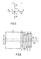
- FIG. 5 are shown in the same plane P the emitting or receiving surfaces of the light waveguides whose signals are intended to be coupled by the device according to the invention.
- the emitting or receiving surfaces of the light waveguides whose signals are intended to be coupled by the device according to the invention.
- the ends of the light waveguides have surfaces of small dimensions, generally of the order of a tenth of a millimeter in diameter. Under these conditions, these surfaces can be assimilated to their center represented by one of the points W or W 1 , W 2 , W 3 , W 4 .
- FIG. 5 shows that, according to the invention, these ends are fixed in the same plane P.
- the four ends W 1 , W 2 , W 3 , W 4 are distributed around the end W, equidistant from the latter, and placed on two perpendicular axes passing through the end W.
- the ends W 1 and W 2 are thus on the axis 15 and the ends W 3 and W 4 on the axis 16.
- the different guides wave are all perpendicular to the plane P at their end.
- FIGS 1 and 2 illustrate the principle according to which the present coupling device operates.
- a light beam of wavelength ⁇ 1 + ⁇ 2 + ⁇ 3 + ⁇ 4 strikes a first spherical surface 45 coated with an interference filter capable of reflecting rays of wavelength ⁇ 1 .
- the center of curvature of the surface 45 being the point Ci located in the plane P in the middle of the segment defined by the end W and the end W i , the rays coming from W and of wavelength ⁇ 1 are reflected by the surface 45 on the end W i .
- the rays of wavelength ⁇ 2 + ⁇ 3 + ⁇ 4 are transmitted and strike the spherical surface 46 coated with an interference filter capable of reflecting the rays of wavelength ⁇ 2 .
- the center of curvature of the surface 46 being the point C 2 located in the plane P in the middle of the segment defined by the end W and the end W 2 , the rays coming from W and of wavelength ⁇ 2 are reflected by the surface 46 on the end W 2 .
- the rays of wavelength ⁇ 3 + ⁇ 4 are transmitted by the surface 46.
- the rays of wavelength ⁇ 3 are reflected on the end W 3 by a spherical surface 47 of center of curvature C 3 situated in the plane P in the middle of the segment WW 3 , this surface being coated with a interference filter capable of reflecting light rays of wavelength ⁇ 3 .
- the light rays of wavelength ⁇ 4 are transmitted and strike a last spherical surface 48 with center of curvature C 4 located in the middle of the segment WW 4 .
- This last surface 48 can be coated with a totally reflecting mirror.
- the surface 48 can also be coated with an interference filter capable of reflecting the light rays of wavelength ⁇ 4 and letting the others pass. The latter solution eliminates parasitic radiation.
- the number of wavelengths conveyed is not limiting. If this number is N, it will suffice to use N spherical surfaces as defined above.
- the coupling will then be between an end waveguide W and N end waveguides W 1 , W 2 ... W N , respectively transporting the wavelengths ⁇ 1 , ⁇ 2 ... ⁇ N.
- a first embodiment of the device according to the invention is shown in Figure 3, in section perpendicular to the plane P along the axis 15, and Figure 4 in section perpendicular to the plane P along the axis 16. It consists of four pairs of lenses. Each pair is formed of lenses, respectively convex plane and concave plane, of transparent material, joined together according to a common spherical diopter and forming a blade with faces parallel to each other and to the plane P. This diopter is coated with an interference filter reflecting one wavelengths ⁇ 1 to 4 and transparent to other wavelengths, or a mirror reflecting all the wavelengths ⁇ 1 to ⁇ 4 .
- these pairs of convex plane and concave plane lenses are respectively 41, 42, 43, 44, their spherical diopter being 45, 46, 47, 48 respectively.
- the diopters 45, 46, 47 are coated with a interference filter reflecting respectively the wavelengths A ,, A 2 , ⁇ 3 and transparent to the other wavelengths.
- the diopter 48 is provided with a mirror reflecting all the wavelengths ⁇ 1 to ⁇ 4 .
- the optical axes of the constituent lenses of each plate respectively 49, 50, 51, 52 are perpendicular to the plane P. These axes intersect, in this plane, the segments WW 1 , WW 2 , WW 3 , WW 4 respectively in their middle C 1 , C 2 , C 3 , C 4 .
- the radius R 3 of the diopter 47 satisfies the relation: where E 1 and E 2 represent the thickness respectively of the glass blades 41 and 42.13 the thickness of the convex plane lens of the blade 43, l 0 the thickness of the medium preceding the blade 41 and located between the plane P and the blade 41, 1 3 and 1 0 being both measured on the axis 51, n the refractive index of the material constituting the different blades and n o that of the medium preceding the blade 41.
- the diopters 45,46,48 satisfy similar relationships.
- the points C 1 , C 2 , C 3 , C 4 are therefore, in this embodiment, the antinodal points of the thick lenses whose diopter is respectively 45, 46, 47, 48. From these thick lenses, the end W is optical conjugation of the ends respectively W 1 , W 2 , W 3 , W 4 . Similarly, any beam from W 1 , W 2 , W 3 , W 4 , such as the beams respectively 53, 54, 55, 56 of wavelengths respectively ⁇ 1 , ⁇ 2 , ⁇ 3 , ⁇ 4 converges on l 'W end and vice versa.
- the radius R 3 is then given by the relation:
- the centers of curvature of the diopters 45, 46, 47, 48 are located upstream of the plane of the ends of the tracks on the respective axes 49, 50, 51, 52.
- FIG. 6 shows in section a variant of this embodiment for which the medium preceding the blade 41 consists of the block 53 made of glass with a refractive index n, of the same nature as the glass constituting the various blades.
- the centers of curvature of the diopters 45 to 48 are then located in the plane P of the ends of the waveguides and merged with the antinodal points respectively C 1 , C 2 , C 3 , C 4 of the lenses explained above.
- the presence of this block of glass 53 improves the quality of the image reflected by each interference filter or mirror (absence of so-called spherical aberration at the air-glass interface of the first face of the reference block 41 of FIGS. 3 and 4).
- this very compact assembly allows the installation of an adaptation liquid between the glass faces and at the level of the inlet face of the block 53, which leads to a reduction in Fresnel losses.
- the various lenses can be made of borosilicate.
- the interference filters are produced on such a support by depositing layers in an odd number of materials of alternately high index and low index, transparent in the wavelength range envisaged, the deposit starting with a layer of high index.
- an interference filter reflecting in the wavelength range between 0.8 and 1 ⁇ m and transparent outside this range can be produced by a succession of 31 alternating layers of oxide of titanium Ti0 2 and silicon oxide SiO 2 , titanium oxide being the high index material and silicon oxide being the low index material.
- Thicknesses of layers making it possible to produce such filters more particularly centered on a chosen wavelength are well known to those skilled in the art.
- the coupling device produced in accordance with the present invention brings many advantages. Its implementation is particularly easy because it comprises only one type of means for obtaining both the spatial selection and the spectral selection of the beams, these means being simple spherical semi-reflecting surfaces. These surfaces are themselves easy to obtain by manufacturing the optical doublets described. The adjustment of the system is easy since it is done by displacement of these pairs of lenses relative to each other, parallel to the plane P. It is indeed much easier to move and adjust conventional optical systems than guides wave or optical fibers. Finally, this device does not limit the range of wavelengths of the transported signals.
Landscapes
- Physics & Mathematics (AREA)
- General Physics & Mathematics (AREA)
- Optics & Photonics (AREA)
- Optical Couplings Of Light Guides (AREA)
- Glass Compositions (AREA)
- Mechanical Coupling Of Light Guides (AREA)
Claims (4)

Applications Claiming Priority (2)
| Application Number | Priority Date | Filing Date | Title |
|---|---|---|---|
| FR8304042A FR2542461B1 (fr) | 1983-03-11 | 1983-03-11 | Dispositif optique de multiplexage demultiplexage |
| FR8304042 | 1983-03-11 |
Publications (3)
| Publication Number | Publication Date |
|---|---|
| EP0121962A2 EP0121962A2 (de) | 1984-10-17 |
| EP0121962A3 EP0121962A3 (en) | 1987-11-19 |
| EP0121962B1 true EP0121962B1 (de) | 1990-10-03 |
Family
ID=9286766
Family Applications (1)
| Application Number | Title | Priority Date | Filing Date |
|---|---|---|---|
| EP84200313A Expired - Lifetime EP0121962B1 (de) | 1983-03-11 | 1984-03-06 | Vorrichtung zur optischen Kopplung zwischen Lichtwellenleitern |
Country Status (5)
| Country | Link |
|---|---|
| US (1) | US4735478A (de) |
| EP (1) | EP0121962B1 (de) |
| JP (1) | JPS59172623A (de) |
| DE (1) | DE3483333D1 (de) |
| FR (1) | FR2542461B1 (de) |
Families Citing this family (12)
| Publication number | Priority date | Publication date | Assignee | Title |
|---|---|---|---|---|
| GB8523407D0 (en) * | 1985-09-23 | 1985-10-30 | Plessey Co Plc | Fibre-optic tapping assemblage |
| US5000531A (en) * | 1989-05-22 | 1991-03-19 | Harris Corporation | Passive bypass for fiber optic ring network |
| US5218656A (en) * | 1991-03-04 | 1993-06-08 | Specac Ltd. | Optical fiber probe for attentuated total reflectance measurements |
| US5355237A (en) * | 1993-03-17 | 1994-10-11 | The United States Of America As Represented By The Administrator Of The National Aeronautics And Space Administration | Wavelength-division multiplexed optical integrated circuit with vertical diffraction grating |
| US6046854A (en) * | 1996-02-09 | 2000-04-04 | Corning Incorporated | Multi-path interference filter with reflective surfaces |
| US5841583A (en) * | 1996-02-09 | 1998-11-24 | Corning Incorporated | Multi-path interference filter |
| US6111674A (en) * | 1996-02-23 | 2000-08-29 | Corning Incorporated | Multiple reflection multiplexer and demultiplexer |
| JP3917698B2 (ja) * | 1996-12-12 | 2007-05-23 | 株式会社半導体エネルギー研究所 | レーザーアニール方法およびレーザーアニール装置 |
| JPH10253916A (ja) * | 1997-03-10 | 1998-09-25 | Semiconductor Energy Lab Co Ltd | レーザー光学装置 |
| US6018603A (en) * | 1997-09-05 | 2000-01-25 | Lundgren; Kent R. | Optical demultiplexing/multiplexing device having a wavelength dependent element |
| US6341040B1 (en) * | 1999-06-08 | 2002-01-22 | Jds Uniphase Corporation | Multi-plate comb filter and applications therefor |
| DE102008042234A1 (de) * | 2008-09-19 | 2010-04-01 | Carl Zeiss Ag | Filterelement und Aufnahmevorrichtung mit einem Filterelement |
Family Cites Families (8)
| Publication number | Priority date | Publication date | Assignee | Title |
|---|---|---|---|---|
| US4304460A (en) * | 1978-03-10 | 1981-12-08 | Matsushita Electric Industrial Co., Ltd. | Optical switching device |
| US4294508A (en) * | 1979-08-22 | 1981-10-13 | The United States Of America As Represented By The Secretary Of The Air Force | Optical multiplexer/demultiplexer |
| US4274706A (en) * | 1979-08-30 | 1981-06-23 | Hughes Aircraft Company | Wavelength multiplexer/demultiplexer for optical circuits |
| DD148390B1 (de) * | 1979-12-28 | 1987-04-08 | Claus Renschen | Anordnung zum einkoppeln von licht in einem lichtleiter |
| DE3019956A1 (de) * | 1980-05-24 | 1981-12-03 | Ibm Deutschland Gmbh, 7000 Stuttgart | Modulares, faseroptisches kommunikationssystem |
| CA1154987A (en) * | 1981-11-27 | 1983-10-11 | Narinder S. Kapany | Fiber optics commmunications modules |
| US4474424A (en) * | 1981-03-20 | 1984-10-02 | At&T Bell Laboratories | Optical multi/demultiplexer using interference filters |
| CA1249466A (en) * | 1983-01-31 | 1989-01-31 | Narinder S. Kapany | Fiber optics communication modules |
-
1983
- 1983-03-11 FR FR8304042A patent/FR2542461B1/fr not_active Expired
-
1984
- 1984-03-06 EP EP84200313A patent/EP0121962B1/de not_active Expired - Lifetime
- 1984-03-06 DE DE8484200313T patent/DE3483333D1/de not_active Expired - Lifetime
- 1984-03-09 JP JP59044208A patent/JPS59172623A/ja active Pending
-
1987
- 1987-01-12 US US07/005,380 patent/US4735478A/en not_active Expired - Fee Related
Also Published As
| Publication number | Publication date |
|---|---|
| JPS59172623A (ja) | 1984-09-29 |
| FR2542461B1 (fr) | 1987-01-23 |
| US4735478A (en) | 1988-04-05 |
| EP0121962A2 (de) | 1984-10-17 |
| EP0121962A3 (en) | 1987-11-19 |
| FR2542461A1 (fr) | 1984-09-14 |
| DE3483333D1 (de) | 1990-11-08 |
Similar Documents
| Publication | Publication Date | Title |
|---|---|---|
| EP0121482B1 (de) | Wellenlängenmultiplexer/-demultiplexer und Verfahren zur Herstellung einer solchen Vorrichtung | |
| EP0022008B1 (de) | Optisches Relais zur Bildübertragung zwischen Punkten auf einer optischen Achse | |
| EP0138698B1 (de) | Optischer Wellenlängen-Multiplexer-Demultiplexer für bidirektionale Verbindung | |
| EP0275795B1 (de) | Wellenlängen-Multiplexer/-Demultiplexer mit einem elliptischen Konkavgitter und dessen Anwendung in der integrierten Optik | |
| EP0196963B1 (de) | Gegen geometrische und chromatische Aberrationen korrigierter Wellenlängen-Multiplexer/-Demultiplexer | |
| EP0562953B1 (de) | Durch Rotation abstimmbares Fabry-Perot-Interferometor enthaltendes optisches Filter | |
| EP0072840B1 (de) | Verfahren zum multiplexen von übertragungskanälen in einer optischen faser mit stufen-index und vorrichtung zur durchführung des verfahrens | |
| FR2558607A1 (fr) | Demultiplexeur optique de longueurs d'ondes | |
| EP0557162A1 (de) | Holographisches Strahlenschutzfilter, besonders für Laser | |
| EP0102264B1 (de) | Anordnung zur Wellenlängen Multiplexierung oder Demultiplexierung mit optischer Trennung | |
| EP0121962A2 (de) | Vorrichtung zur optischen Kopplung zwischen Lichtwellenleitern | |
| EP0782021A1 (de) | Optischer Demultiplexer mit Wellenleiter-Gitter | |
| FR2834565A1 (fr) | Dispositif pour faire entrer des signaux optiques dans un guide d'ondes de lumiere et/ou pour les en faire sortir | |
| EP3237860A1 (de) | Weitfeld-infrarot-bildgebungssystem | |
| EP1509794B1 (de) | Optische filtrierungseinrichtung | |
| EP3899458B1 (de) | Instrument mit mehreren optischen kanälen | |
| EP1546770B1 (de) | Optische filterkomponente mit flacher oberseite | |
| EP3525015A1 (de) | Optisches monoblockelement mit diaphragma | |
| EP0214045B1 (de) | Optisches Gerät mit selektivem Spektralfilter | |
| FR2532766A1 (fr) | Dispositif de couplage optique | |
| EP0553583A1 (de) | Infrarotkamera mit selbsttemperaturkompensiertem optischem System | |
| EP0416989B1 (de) | Kopplungsvorrichtung zwischen optischen Übertragungselementen | |
| FR2561003A1 (fr) | Dispositif optique rotateur d'image | |
| WO2025082939A1 (fr) | Dispositif de mesure confocale chromatique à bloc séparateur | |
| WO2025114340A1 (fr) | Assemblage optique à fibre optique |
Legal Events
| Date | Code | Title | Description |
|---|---|---|---|
| PUAI | Public reference made under article 153(3) epc to a published international application that has entered the european phase |
Free format text: ORIGINAL CODE: 0009012 |
|
| AK | Designated contracting states |
Designated state(s): DE FR GB IT SE |
|
| PUAL | Search report despatched |
Free format text: ORIGINAL CODE: 0009013 |
|
| RHK1 | Main classification (correction) |
Ipc: G02B 6/34 |
|
| AK | Designated contracting states |
Kind code of ref document: A3 Designated state(s): DE FR GB IT SE |
|
| 17P | Request for examination filed |
Effective date: 19880502 |
|
| 17Q | First examination report despatched |
Effective date: 19880712 |
|
| RAP1 | Party data changed (applicant data changed or rights of an application transferred) |
Owner name: N.V. PHILIPS' GLOEILAMPENFABRIEKEN Owner name: LABORATOIRES D'ELECTRONIQUE PHILIPS |
|
| GRAA | (expected) grant |
Free format text: ORIGINAL CODE: 0009210 |
|
| AK | Designated contracting states |
Kind code of ref document: B1 Designated state(s): DE FR GB IT SE |
|
| PG25 | Lapsed in a contracting state [announced via postgrant information from national office to epo] |
Ref country code: SE Effective date: 19901003 Ref country code: IT Free format text: LAPSE BECAUSE OF FAILURE TO SUBMIT A TRANSLATION OF THE DESCRIPTION OR TO PAY THE FEE WITHIN THE PRESCRIBED TIME-LIMIT;WARNING: LAPSES OF ITALIAN PATENTS WITH EFFECTIVE DATE BEFORE 2007 MAY HAVE OCCURRED AT ANY TIME BEFORE 2007. THE CORRECT EFFECTIVE DATE MAY BE DIFFERENT FROM THE ONE RECORDED. Effective date: 19901003 Ref country code: GB Effective date: 19901003 |
|
| REF | Corresponds to: |
Ref document number: 3483333 Country of ref document: DE Date of ref document: 19901108 |
|
| GBV | Gb: ep patent (uk) treated as always having been void in accordance with gb section 77(7)/1977 [no translation filed] | ||
| PLBE | No opposition filed within time limit |
Free format text: ORIGINAL CODE: 0009261 |
|
| STAA | Information on the status of an ep patent application or granted ep patent |
Free format text: STATUS: NO OPPOSITION FILED WITHIN TIME LIMIT |
|
| 26N | No opposition filed | ||
| PG25 | Lapsed in a contracting state [announced via postgrant information from national office to epo] |
Ref country code: FR Effective date: 19911129 |
|
| PG25 | Lapsed in a contracting state [announced via postgrant information from national office to epo] |
Ref country code: DE Effective date: 19920101 |
|
| REG | Reference to a national code |
Ref country code: FR Ref legal event code: ST |