EP0122637A2 - Automatischer adaptiver Entzerrer - Google Patents
Automatischer adaptiver Entzerrer Download PDFInfo
- Publication number
- EP0122637A2 EP0122637A2 EP84104389A EP84104389A EP0122637A2 EP 0122637 A2 EP0122637 A2 EP 0122637A2 EP 84104389 A EP84104389 A EP 84104389A EP 84104389 A EP84104389 A EP 84104389A EP 0122637 A2 EP0122637 A2 EP 0122637A2
- Authority
- EP
- European Patent Office
- Prior art keywords
- delay
- signal
- equalizer
- signals
- amplitude
- Prior art date
- Legal status (The legal status is an assumption and is not a legal conclusion. Google has not performed a legal analysis and makes no representation as to the accuracy of the status listed.)
- Granted
Links
- 230000003044 adaptive effect Effects 0.000 title claims description 19
- 238000007792 addition Methods 0.000 claims description 4
- 230000005540 biological transmission Effects 0.000 claims description 4
- 230000008054 signal transmission Effects 0.000 abstract description 3
- 238000010586 diagram Methods 0.000 description 10
- 230000001934 delay Effects 0.000 description 4
- 230000003111 delayed effect Effects 0.000 description 3
- 238000012935 Averaging Methods 0.000 description 2
- 238000012986 modification Methods 0.000 description 1
- 230000004048 modification Effects 0.000 description 1
- 238000001228 spectrum Methods 0.000 description 1
Images


Classifications
-
- H—ELECTRICITY
- H04—ELECTRIC COMMUNICATION TECHNIQUE
- H04L—TRANSMISSION OF DIGITAL INFORMATION, e.g. TELEGRAPHIC COMMUNICATION
- H04L27/00—Modulated-carrier systems
- H04L27/01—Equalisers
Definitions
- the present invention relates to an automatic adaptive equalizer, and more specifically to such an equalizer featuring improvements in equalizing delay and amplitude distortions of an incoming signal according to control signals obtained from baseband signals.
- Another object of the present invention is to provide an automatic adaptive equalizer, which equalizes or conditions at least one of amplitude and delay distortions according to control signals obtained from a demodulator.
- Still another object of the present invention is to provide an automatic adaptive equalizer which cancels intersymbol interference and also equalizes at least one of amplitude and delay distortions, according to control signals obtained from a demodulator (viz., baseband signals).
- Still another object of the present invention is to provide an automatic adaptive equalizer featuring improvements in equalizing delay, amplitude distortions of an incoming signal through a simple circuit configuration.
- an automatic adaptive equalizer wherein in order to remove at least one of amplitude and delay distortions which tend to occur during signal transmission, there is provided circuitry wherein a received IF digital signal is fed through an equalizer circuit to a demodulator and wherein the demodulator outputs a series of data and error signals to a control signal generator.
- the control signal generator produces in-phase and quadrature control signals which are appropriately added and subtracted and subsequently averaged in an adder and subtracter circuit before being applied to a series of equalizers in the equalizer circuit.
- the present invention takes a form of an automatic adaptive equalizer for use in a digital radio transmission system, comprising: a first means for equalizing at least one of amplitude and delay distortions of an incoming IF signal; a demodulator being supplied with'the output of the first means, and generating a plurality of data signals and a plurality of error signals; a control signal generator receiving the plurality of data signals and the plurality of error signals, and generating a plurality of in-phase control signals and a plurality of quadrature control signals; a second means for receiving and performing additions and subtractions of selected ones of the in-phase and quadrature control signals, and for applying the results of the addition and subtractions to the first means.
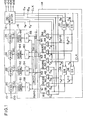
- Fig. 1 shows in block diagram form a first embodiment of the automatic adaptive equalizer according to the present invention.
- the Fig. 1 arrangement generally comprises an adaptive equalizer circuit 10, a demodultor 12, a control signal generator 14 and an adder/subtracter circuit 16.
- the adaptive equalizer circuit 10 includes four equalizers arranged to compensate for delay and amplitude distortions of an incoming IF (Intermediate Frequency) digital signal applied thereto via an input terminal 100. More specifically, the four equalizers of the circuit 10 are a parabolic (or second-order) delay distortion equalizer 20, a linear delay distortion equalizer 22, a linear amplitude distortion equalizer 24 and a parabolic amplitude equalizer 26.
- the demodulator 12 includes, although not shown, a phase detector, a level discriminator, an error signal generator, a clock synchronizer, etc.
- the control signal geneator 14 comprises shift registers 30, 32, 34 and 36, exclusive-OR gates 38, 40, 42, 44, 46 and 48, and exclusive-NOR gates 50 and 52, and resistors Rl, R2, R3, R4, R5, R6, R7 and R8, all of which are coupled as shown.
- the adder/subtracter circuit 16 includes adders 54, 56, subtracters 58, 60, and averaging circuits 60, 62, 64 and 66. Each of the latter mentioned circuits may take the form of an integrator.
- the adaptive equalizer circuit 10 is supplied with the IF digital signal via the terminal 100, and conditions or compensates for the linear and parabolic delay distortions of the incoming IF signal in the equalizers 22 and 20, respectively, and further compensates for the linear and parabolic amplitude distortions of the incoming IF signal in the equalizers 24 and 26, respectively.
- the delay and amplitude equalizations in the equalizers 20, 22, 24 and 26 are controlled by control signals D2, Dl, A2 and Al, respectively, which are applied from the adder/subtracter circuit 16.
- the circuit 10 supplies the output thereof to the demodulator 12, which outputs demodulated signals (baseband signals) over lines 102, 104, 106 and 108 and which also outputs data signals Dp, Dq, error signals Yp, Yq, and clocks (CLK) for use in equalizing the aforementioned distortions of the incoming signal.
- the signals Dp, Dq, Yp, Yq, and clocks CLK are applied to the control signal generator 14.
- the shift registers 30 and 32 are respectively supplied with the data signals Dp and Dq in addition to clocks CLK, and thence respectively generate data signals Dp(-l) and Dq(-l), wherein (-1) denotes a delay by one bit relative to the corresponding incoming data signal.
- the shift registers 34 and 36 respectively receive the error signals Yp and Yq with clocks CLK, and thence respectively generate error signals Yp(-l) and Yq(-l), wherein (-1) denotes a delay by one bit relative to the corresponding incoming error signal.
- the data signal Dp is directly applied to the exclusive OR gates 38 and 42, and, the other data signal Dq directly to the exclusive OR gate 40 and the exclusive NOR gate 50, as shown in the drawing.
- the error signal Yp is directly applied to the exclusive OR gate 44 and the exclusive NOR gate 52, and, the other error signal Yq directly to the exclusive OR gates 46 and 48.
- the outputs of the gates 38 and 40 are added at a node Nl and applied to the subtracter 58 as an in-phase control signal Re(+l), while the outputs of the gates 42 and 50 are added at a node N2 and applied to the adder 54 as a quadrature control signal Im(+l).
- control signals Re(+l), Im(+l), Re(-l) and Im(-l) are given by following equations(l): Wherein (a) the suffixes (+l) and (-1) attached to Re (and Im) respectively denote that the data signal Dp is advanced and delayed by one bit relative to the error signal Yp, and (b) ".” denotes a logic operation of exclusive OR.
- the subtracters 58, 60 and the adders 54, 56 generate control signals, respectively, which are respectively averaged in the associated averaging circuits 62, 60, 66 and 64, and which are applied to the adaptive equalizer circuit 10 as the control signals D2, A2, Dl and Al, respectively.
- the values of the control signals Dl, D2, Al and A2 are given by following equations(2):
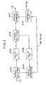
- Fig. 2 is a block diagram showing one example of a circuit arrangement which may be used as each of the linear and parabolic amplitude distortion equalizers 26 and 24.
- an IF input signal is the output of the linear delay equalizer 22. Otherwise, the IF input signal is the output of the equalizer 24.
- the Fig. 2 arrangement is disclosed in U.S. patent No. 4,333,063 assigned to the assignee of the present invention.
- the IF input signal is fed to a signal splitter 200 via an input terminal 110.
- the signal splitter 200 along with other signal splitter 204, simply divides the input signal into two outgoing signals.
- One of the outputs of the splitter 200 is applied via a delay device 202 to the signal splitter 204.
- the other output of the signal splitter 200 is applied to a signal-combining circuit 206.
- One of the two outputs from the signal splitter 204 is applied to the combining circuit 206 via a delay device 208, the delays in the delay devices 202 and 208 being identical.
- the signal combiner 206 generates a sum signal which is applied to a control circuit 210 which controls the amplitude and polarity of the signal applied thereto according to the control signal Al or A2.
- the output of the control circuit 210 is applied to one of the inputs of a signal combiner 212, which receives the other output of the signal splitter 204.
- the output of the signal combiner 212 is the output of the equalizer.
- Each of the signal splitters 200, 204 and the signal combiners 206, 212 is of well known configuration.
- the delay T in each of the delay devices 202 and 208 is set as follows: wherein (a) f 0 denotes a center frequency of the input signal applied to the terminal 110 and (b) m is a positive integer. Accordingly, the transfer function (4) is a function of sine so that an approximately linear slope is obtainable in the vicinity of f 0 .
- the delay T in each of the delay devices 202 and 208 is set as follows: The transfer function (4) is a function of cosine, whereby an approximately parabolic curve is obtained in the vicinity of f 0 .
- linear and parabolic amplitude distortions of an input signal are adaptively compensated for in the equalizers 22 and 20.
- Fig. 3 is a block diagram showing a second example of circuitry which is usable as the linear delay distortion equalizer 22 of Fig. 1.
- An IF input signal which is the output of the equalizer 20 shown in Fig. 1, is applied via an input terminal 114 to one input of a first subtracter 300.
- the IF input signal is also delayed in four delay devices 302, 304, 306 and 308 in tandem, and thence is applied to the other input of the subtracter 300.
- the delay device 302 applies the output thereof to one input of a second subtracter 310 which receives at the other input the output of the delay device 306.
- the delay device 306 supplies a signal combiner 312 with the output thereof.
- Each of the subtracters 300 and 310 performs a subtraction between the amplitudes of the two signals applied.
- a signal combiner 314 adds the outputs of the subtracters 302 and 304, and applies the output thereof to a control circuit 316 which controls the amplitude and polarity of the signal applied according to the control signal Dl. .
- the signal combiner 312 adds the outputs of the circuit 316 and the delay device 304, and outputs the output over a line 116 which is coupled via an output terminal 118 to the input of the equalizer 24.
- Fig. 4 is a sketch showing delay characteristics obtained using equation (6) in terms of frequency vs. delay wherein the parameter is the amplitude control coefficient ⁇ .
- f denotes a lower frequency which corresponds to a frequency in the vicinity of and higher than the lower band edge of the IF input signal
- f denotes an upper frequency which corresponds to a frequency in the vicinity of and lower than the upper band edge of the IF input signal.
- Fig. 5 is a block diagram showing one example of circuitry which is usable as the parabolic delay distortion equalizer 20 of Fig. 1.
- the IF input signal is applied via the input terminal 100 to one input of a subtracter 400.
- the IF input signal is also delayed in delay devices 402 and 404 in tandem, and thence is applied to the other input of the subtracter 400.
- the delay device 402 applies the output thereof to one input of a signal combiner 406, and the delay device 404 applies the output thereof to the other input of the subtracter 400.
- the subtracter 400 performs a subtraction between the amplitudes of the two signals applied, and thence applies the output thereof to a control circuit 408 which controls the amplitude and porality of the signal applied to the signal combiner 406 according to the control signal D2.
- the signal combiner 406 adds the outputs of the control circuit 408 and the delay device 402, and applies an output via line 120 and output terminal 122 to the input of the equalizer 22.
- Fig. 6 is a sketch showing delay characteristics of the equation (7) in terms of frequency vs. delay wherein the parameter is the amplitude control coefficient ⁇ .
- Fig. 7 shows in block diagram form a second embodiment of the present invention. This embodiment is directed to the cancellaton of intersymbol interference, plus the equalizations of delay and amplitude distortions which are referred to in connection with the first embodiment.
- the Fig. 7 arrangement generally comprises an adaptive equalizer circuit 10', a demodultor 12', a control signal generator 14', an adder/subtracter circuit 16', and a transversal filter 500.
- the Fig. 7 embodiment differs from that of Fig. 1 by the inclusion of a transversal filter 500.
- the blocks 10' and 16 1 are substantially identical with the blocks 10 and 16 of Fig. 1, respectively.
- the blocks 12' and 14' are similar to the blocks 12 and 14 of Fig. 1, but are modified so as to generate additional error signals Yp', Yq' and control signal Re(0).
- the demodulator 12' generates the data signals Dp, Dq, and the error signals Yp, Yq, Yp', Yq', all of which are applied to the control signal generator 14'.
- the demodulator 12' also outputs the baseband signals over the lines 102, 104, 106 and 108 as previously referred to in connection with Fig. 1.
- the control signal generator 14' is arranged to generate the control signal Re(0) which is applied to the transversal filter 500.
- the other control signals Re(+l), Im(+l), Re(-l) and Im(-l) are identical with the corresponding control signals mentioned in the first embodiment, and are applied to the adder/subtracter 16' and also to the transversal filter 500.
- the portion enclosed by a broken line 502 is already referred to in the first embodiment.
- the control signal Re(0) is obtained by similar circuitry by which Re(+l) and Re(-l) are generated, and is represented by: Re(0) is used for controlling a variable tap gain controller (not shown) provided for a main tap of the transversal filter 500. While, Re(-l), Im(-l), Re(+l) and Im(+l) are used to control variable tap gain controllers for the taps preceding and immediately following the main tap.
- the in-phase control signal Re(-l) corresponds to the real component of a tap coefficents C(-l) for a tap which immediately precedes the main tap
- the in-phase control signal Re(+l) corresponds to the real component of a tap coefficient C(+l) for the tap immediately following the main tap
- the quadrature control signals Im(-l) and Im(+1) respectively correspond to the imaginary components of the tap coefficient C(-l) and C(+l).
- the first embodiment shown in Fig. 1 includes the four equalizers 20, 22, 24 and 26.
- the present invention is not limited to this arrangement, but is capable of selectively employing one or more than two equalizers on the case-by-case basis considering practical transmission distortions.
Landscapes
- Engineering & Computer Science (AREA)
- Computer Networks & Wireless Communication (AREA)
- Signal Processing (AREA)
- Cable Transmission Systems, Equalization Of Radio And Reduction Of Echo (AREA)
- Filters That Use Time-Delay Elements (AREA)
Applications Claiming Priority (2)
| Application Number | Priority Date | Filing Date | Title |
|---|---|---|---|
| JP68635/83 | 1983-04-19 | ||
| JP58068635A JPS59194540A (ja) | 1983-04-19 | 1983-04-19 | 自動適応型等化器 |
Publications (3)
| Publication Number | Publication Date |
|---|---|
| EP0122637A2 true EP0122637A2 (de) | 1984-10-24 |
| EP0122637A3 EP0122637A3 (en) | 1987-04-15 |
| EP0122637B1 EP0122637B1 (de) | 1990-07-11 |
Family
ID=13379387
Family Applications (1)
| Application Number | Title | Priority Date | Filing Date |
|---|---|---|---|
| EP84104389A Expired EP0122637B1 (de) | 1983-04-19 | 1984-04-18 | Automatischer adaptiver Entzerrer |
Country Status (5)
| Country | Link |
|---|---|
| US (1) | US4638495A (de) |
| EP (1) | EP0122637B1 (de) |
| JP (1) | JPS59194540A (de) |
| CA (1) | CA1218120A (de) |
| DE (1) | DE3482668D1 (de) |
Cited By (1)
| Publication number | Priority date | Publication date | Assignee | Title |
|---|---|---|---|---|
| GB2293948A (en) * | 1994-09-27 | 1996-04-10 | Fujitsu Ltd | Digitally controlled automatic amplitude equalizers |
Families Citing this family (13)
| Publication number | Priority date | Publication date | Assignee | Title |
|---|---|---|---|---|
| DE3765947D1 (de) * | 1986-01-18 | 1990-12-13 | Hewlett Packard Ltd | Beeinflussungsfreier analysator zur erfassung von kanalstoerungen. |
| JPS6367829A (ja) * | 1986-09-09 | 1988-03-26 | Matsushita Electric Ind Co Ltd | デイジタル情報伝送装置 |
| US4812995A (en) * | 1987-05-19 | 1989-03-14 | Girgis Adly A | Adaptive Kalman Filtering in fault classification |
| JPH01126760A (ja) * | 1987-11-11 | 1989-05-18 | Toshiba Corp | 並列計算機システム |
| JPH02104121A (ja) * | 1988-10-13 | 1990-04-17 | Nec Corp | トランスバーサル型等化器 |
| JP2952947B2 (ja) * | 1989-03-31 | 1999-09-27 | 日本電気株式会社 | 隣接干渉除去装置 |
| DE3916256A1 (de) * | 1989-05-18 | 1990-11-22 | Ant Nachrichtentech | Digitalfilter mit daempfungs- und phasengangentzerrung |
| DE3916236A1 (de) * | 1989-05-18 | 1990-11-22 | Ant Nachrichtentech | Digitalfilter mit daempfungs- und phasengangentzerrung |
| JP2616123B2 (ja) * | 1990-03-30 | 1997-06-04 | 日本電気株式会社 | 自動適応形等化器 |
| FR2714782B1 (fr) * | 1993-12-30 | 1996-02-02 | Alcatel Telspace | Estimateur en bande de base de la caractéristique amplitude/fréquence d'un signal à pluralités de phases. |
| US6088388A (en) * | 1997-09-16 | 2000-07-11 | Tektronix, Inc. | Digital fir filters for compensation of nyquist slope in pseudo-synchronous demodulators |
| US6879630B2 (en) * | 2000-03-30 | 2005-04-12 | Hitachi Kokusai Electric Inc. | Automatic equalization circuit and receiver circuit using the same |
| JP4016143B2 (ja) * | 2003-01-29 | 2007-12-05 | ソニー株式会社 | 再生信号波形処理装置及び再生信号波形処理方法 |
Family Cites Families (8)
| Publication number | Priority date | Publication date | Assignee | Title |
|---|---|---|---|---|
| BE793458A (fr) * | 1971-12-30 | 1973-06-28 | Philips Nv | Dispositif d'egalisation automatique |
| US4003006A (en) * | 1975-10-06 | 1977-01-11 | Bell Telephone Laboratories, Incorporated | Pilot tone controlled adaptive amplitude equalizer |
| US4251782A (en) * | 1979-01-17 | 1981-02-17 | Rockwell International Corporation | Multiple tuned circuit correction apparatus |
| US4247940A (en) * | 1979-10-15 | 1981-01-27 | Bell Telephone Laboratories, Incorporated | Equalizer for complex data signals |
| IT1119567B (it) * | 1979-11-08 | 1986-03-10 | Cselt Centro Studi Lab Telecom | Equalizzatore numerico adattativo per ricevitori di segnali dati utilizzanti una modulazione differenziale di fase |
| US4333063A (en) * | 1979-12-03 | 1982-06-01 | Nippon Electric Co., Ltd. | Amplitude equalizer |
| JPS57109089A (en) * | 1980-12-26 | 1982-07-07 | Nec Corp | Initial value resetting circuit for operational amplifier |
| DE3110919C2 (de) * | 1981-03-20 | 1983-07-21 | AEG-Telefunken Nachrichtentechnik GmbH, 7150 Backnang | Amplituden- und Laufzeitentzerrer |
-
1983
- 1983-04-19 JP JP58068635A patent/JPS59194540A/ja active Granted
-
1984
- 1984-04-18 EP EP84104389A patent/EP0122637B1/de not_active Expired
- 1984-04-18 DE DE8484104389T patent/DE3482668D1/de not_active Expired - Lifetime
- 1984-04-18 CA CA000452280A patent/CA1218120A/en not_active Expired
- 1984-04-19 US US06/601,885 patent/US4638495A/en not_active Expired - Lifetime
Cited By (3)
| Publication number | Priority date | Publication date | Assignee | Title |
|---|---|---|---|---|
| GB2293948A (en) * | 1994-09-27 | 1996-04-10 | Fujitsu Ltd | Digitally controlled automatic amplitude equalizers |
| GB2293948B (en) * | 1994-09-27 | 1999-05-19 | Fujitsu Ltd | Automatic amplitude equalizer |
| US5978415A (en) * | 1994-09-27 | 1999-11-02 | Fujitsu Limited | Automatic amplitude equalizer |
Also Published As
| Publication number | Publication date |
|---|---|
| EP0122637B1 (de) | 1990-07-11 |
| CA1218120A (en) | 1987-02-17 |
| JPS59194540A (ja) | 1984-11-05 |
| US4638495A (en) | 1987-01-20 |
| DE3482668D1 (de) | 1990-08-16 |
| JPH0427736B2 (de) | 1992-05-12 |
| EP0122637A3 (en) | 1987-04-15 |
Similar Documents
| Publication | Publication Date | Title |
|---|---|---|
| US5394110A (en) | Demodulation system having adaptive matched filter and decision feedback equalizer | |
| JP3616706B2 (ja) | 交差偏波間干渉補償機能を備えた復調器 | |
| US5142552A (en) | Method and apparatus for analog D.C. offset cancellation | |
| US4575862A (en) | Cross-polarization distortion canceller for use in digital radio communication receiver | |
| US4638495A (en) | Automatic adaptive equalizer | |
| US4730343A (en) | Decision feedback equalizer with a pattern detector | |
| US5432522A (en) | Cross polarization interference compensating device comprising decision feedback cross polarization interference cancellers | |
| GB2065427A (en) | Data receivers | |
| WO1983001879A1 (en) | Interference cancellation method and apparatus | |
| JPH10271051A (ja) | 双方向等化を伴う送/受信装置 | |
| EP0055922A1 (de) | Adaptiver Entzerrer für Quadraturamplitudenmodulation | |
| US4308618A (en) | Method of compensating phase noise at the receiver end of a data transmission system | |
| US4926499A (en) | Carrier phase controller for a receiver of phase modulated signals | |
| US4370749A (en) | Phase noise correction circuit for a data transmission system | |
| JPH1174942A (ja) | 無線受信装置 | |
| JPH0447721A (ja) | 自動等化器 | |
| US5285475A (en) | Decision-feedback equalizer capable of producing an equalized signal at high speed | |
| US4306307A (en) | Method of reducing phase noise at the receiver end of a data transmission system | |
| US5121415A (en) | Adjusting filter coefficients | |
| US5790597A (en) | Apparatus and method for interference compensation | |
| JPH0228923B2 (de) | ||
| Goodman et al. | Goodman | |
| JPH0611120B2 (ja) | 自動等化器の等化モード制御方法 | |
| JP2838962B2 (ja) | 搬送波再生方式 | |
| US3999130A (en) | Automatic frequency translator for use with a delay/amplitude equalizer |
Legal Events
| Date | Code | Title | Description |
|---|---|---|---|
| PUAI | Public reference made under article 153(3) epc to a published international application that has entered the european phase |
Free format text: ORIGINAL CODE: 0009012 |
|
| 17P | Request for examination filed |
Effective date: 19840418 |
|
| AK | Designated contracting states |
Designated state(s): DE FR IT NL |
|
| PUAL | Search report despatched |
Free format text: ORIGINAL CODE: 0009013 |
|
| AK | Designated contracting states |
Kind code of ref document: A3 Designated state(s): DE FR IT NL |
|
| 17Q | First examination report despatched |
Effective date: 19881201 |
|
| GRAA | (expected) grant |
Free format text: ORIGINAL CODE: 0009210 |
|
| AK | Designated contracting states |
Kind code of ref document: B1 Designated state(s): DE FR IT NL |
|
| REF | Corresponds to: |
Ref document number: 3482668 Country of ref document: DE Date of ref document: 19900816 |
|
| ET | Fr: translation filed | ||
| ITF | It: translation for a ep patent filed | ||
| ITTA | It: last paid annual fee | ||
| PLBE | No opposition filed within time limit |
Free format text: ORIGINAL CODE: 0009261 |
|
| STAA | Information on the status of an ep patent application or granted ep patent |
Free format text: STATUS: NO OPPOSITION FILED WITHIN TIME LIMIT |
|
| 26N | No opposition filed | ||
| PGFP | Annual fee paid to national office [announced via postgrant information from national office to epo] |
Ref country code: FR Payment date: 20030408 Year of fee payment: 20 |
|
| PGFP | Annual fee paid to national office [announced via postgrant information from national office to epo] |
Ref country code: NL Payment date: 20030429 Year of fee payment: 20 |
|
| PGFP | Annual fee paid to national office [announced via postgrant information from national office to epo] |
Ref country code: DE Payment date: 20030502 Year of fee payment: 20 |
|
| PG25 | Lapsed in a contracting state [announced via postgrant information from national office to epo] |
Ref country code: NL Free format text: LAPSE BECAUSE OF EXPIRATION OF PROTECTION Effective date: 20040418 |
|
| NLV7 | Nl: ceased due to reaching the maximum lifetime of a patent |
Effective date: 20040418 |