EP0122870A2 - Système de transmission de données à portée étendue - Google Patents
Système de transmission de données à portée étendue Download PDFInfo
- Publication number
- EP0122870A2 EP0122870A2 EP19840630061 EP84630061A EP0122870A2 EP 0122870 A2 EP0122870 A2 EP 0122870A2 EP 19840630061 EP19840630061 EP 19840630061 EP 84630061 A EP84630061 A EP 84630061A EP 0122870 A2 EP0122870 A2 EP 0122870A2
- Authority
- EP
- European Patent Office
- Prior art keywords
- mode
- signal
- flip
- data
- gate
- Prior art date
- Legal status (The legal status is an assumption and is not a legal conclusion. Google has not performed a legal analysis and makes no representation as to the accuracy of the status listed.)
- Withdrawn
Links
Images


Classifications
-
- H—ELECTRICITY
- H04—ELECTRIC COMMUNICATION TECHNIQUE
- H04L—TRANSMISSION OF DIGITAL INFORMATION, e.g. TELEGRAPHIC COMMUNICATION
- H04L25/00—Baseband systems
- H04L25/38—Synchronous or start-stop systems, e.g. for Baudot code
- H04L25/40—Transmitting circuits; Receiving circuits
- H04L25/45—Transmitting circuits; Receiving circuits using electronic distributors
-
- G—PHYSICS
- G06—COMPUTING OR CALCULATING; COUNTING
- G06F—ELECTRIC DIGITAL DATA PROCESSING
- G06F13/00—Interconnection of, or transfer of information or other signals between, memories, input/output devices or central processing units
- G06F13/38—Information transfer, e.g. on bus
- G06F13/42—Bus transfer protocol, e.g. handshake; Synchronisation
- G06F13/4204—Bus transfer protocol, e.g. handshake; Synchronisation on a parallel bus
- G06F13/4221—Bus transfer protocol, e.g. handshake; Synchronisation on a parallel bus being an input/output bus, e.g. ISA bus, EISA bus, PCI bus, SCSI bus
- G06F13/4226—Bus transfer protocol, e.g. handshake; Synchronisation on a parallel bus being an input/output bus, e.g. ISA bus, EISA bus, PCI bus, SCSI bus with asynchronous protocol
-
- H—ELECTRICITY
- H04—ELECTRIC COMMUNICATION TECHNIQUE
- H04L—TRANSMISSION OF DIGITAL INFORMATION, e.g. TELEGRAPHIC COMMUNICATION
- H04L25/00—Baseband systems
- H04L25/02—Details ; arrangements for supplying electrical power along data transmission lines
- H04L25/05—Electric or magnetic storage of signals before transmitting or retransmitting for changing the transmission rate
-
- H—ELECTRICITY
- H04—ELECTRIC COMMUNICATION TECHNIQUE
- H04L—TRANSMISSION OF DIGITAL INFORMATION, e.g. TELEGRAPHIC COMMUNICATION
- H04L1/00—Arrangements for detecting or preventing errors in the information received
- H04L1/12—Arrangements for detecting or preventing errors in the information received by using return channel
- H04L1/16—Arrangements for detecting or preventing errors in the information received by using return channel in which the return channel carries supervisory signals, e.g. repetition request signals
- H04L1/1607—Details of the supervisory signal
- H04L1/1671—Details of the supervisory signal the supervisory signal being transmitted together with control information
Definitions
- This invention relates generally to electronic data processing, and pertains more particularly to a system for transmitting digital data over a longer distance than conventional data channels permit.
- this invention contemplates temporary storage of data and special logic to control or facilitate passage of the same to an external device.
- wired data channels vary in length, the length usually being limited to a maximum of about 200 feet. Basically, the distance must be relatively short owing to two factors: (1) circuit limitations and (2) timing limitations.
- Serialization of the data transmission has been a step in the proper direction as far as reducing the above-mentioned circuit limitations. Also, as far as parallel lines are concerned, channel extenders have been devised, these being long line drivers without utilizing serialization; but use of these results in a slowdown of data transfer which can trigger an error condition in a time sequence of demand receiver.
- My invention provides a system for transmitting or transferring digital data over relatively long distances, easily on the order of 0.6 kilometers (2000 feet), and even longer distances, using conducting means, or even radio transmission, if desired. Circuit limitations hereinbefore mentioned are minimized by serializing the data so that all data travels sequentially or over the same path, and preferably by additionally employing suitable modulation techniques to enable the receiver to react to small amplitude signals. In this latter regard, it is preferred that phase modulation be utilized; however, other modulation techniques can be employed depending on the media of transmission.
- a preferred aspect of the invention is to enable transfer of data in the absence of a reply acknowledgment from an external receiver.
- the invention provides logic circuitry that can be incorporated into and used with data processing equipment currently on the market and which equipment need not actually be modified to any degree in order to benefit from the teachings of my invention. Also, the invention preserves system integrity, enabling the transfer of digital data from one vantage point to another without loss or sacrifice of reliability.
- my invention envisages the conversion of the data pulses from a conventional computer to pulses having different and more readily processed voltages.
- the pulses are phase-modulated and then forwarded over a first transmission conduit (e.g., channel) to a receiving station located at a vantage point that can be significantly farther away from the computer end of the transmission than possible heretofore.
- a first transmission conduit e.g., channel
- I employ a phase demodulator and a means for changing the serially received data back to its original form, both as to amplitude and parallelism.
- Buffered storage in the form of a plurality of shift or buffer registers is provided, although such buffer storage can be by-passed when circumstances so dictate.
- These registers are controlled in a manner so that no data will be transmitted unless the registers at the receiving end of my logic can accommodate the data upon receipt. Only a two-bit code need be received before a signal is sent back to the transmitting end of my logic which causes what will be termed an implied acknowledgment signal to be generated, as may be necessary to satisfy the requirements for release of data by an external device at the sending end of my logic.
- the control circuitry for the buffer registers insures that data will be transmitted only as long as they are able to receive and handle such data.
- a preferred but specialized aspect of my invention is that of reducing the number of bits in certain messages or internal acknowledgments transmitted, while at the same time generating at the receiving end the input to an external device of non-transmitted bits, thereby saving time.
- Another preferred but specialized aspect of my invention is that of promptly modifying, under some conditions, some of the output signals of an exterior device (e.g., peripheral unit or computer) into signals accepted by the outputting exterior device, and then directing the modified signals back to the exterior device, without transmission between the exterior devices.
- This technique may be used at both ends and is preferably used where the controlled buffered storage of my invention is employed. It significantly enhances speed of data transfer. While the approach may be looked upon as causing a "lie” to be sent to the exterior devices, even a "lie” generated from their own output, the circuitry controls employed render any such "lie” innocuous and, in fact, highly beneficial in instances where the external device is programmed to require some input before it will release or accept data.
- the entire circuitry making up the logic for both sending and receiving is present in a box or assembly at each end of the conduit for transmission.
- the sending and receiving logic at one end e.g., adjacent a computer
- the assembly of sending and receiving logic at the other end e.g., adjacent a peripheral device
- a digital zero is handled as a minus one volt, whereas a digital one is minus two volts.
- my logic may be employed with any other appropriate electronic significance for conveying the digital data.
- outgoing lines Ml and M2 in Figure 6 may superficially suggest that Mode 1 per se arises from a signal on line Ml, the fact is that the combination of the pulse voltage logic on lines Ml and M2 establishes the "Mode", including Mode 3, and the labeling is done solely for glance recognition.
- My 6 and 12 bit messages may lack--or need not include--service and data signals. To satisfy the needs of the computer and peripheral devices which require those signals for operation, I use the smaller bit messages within my logic to generate appropriate service and data signals as may be required to satisfy the operation of the external devices.
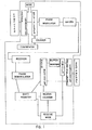
- digital data from an external COMPUTER passes through parallel channels to a LEVEL CONVERTER which merely changes the pulse levels from the computer to a level more readily usable within my logic circuitry, although my logic circuitry may indeed be employed without such conversion, if desired.
- a COMPARATOR samples the parallel stream of data signals from the LEVEL CONVERTER (illustratively what might be called TAG data) and compares that data stream one clock pulse of delay against itself to determine when a change occurs. At the change, a COMPARATOR pulse initiates a COUNTER which starts the MULTIPLEXER operation for serializing the parallel data from the LEVEL CONVERTER.
- Modes 2 and 3 are established by MODE sampling of data from the LEVEL CONVERTER and inserting special lead bits as the beginning bits of any byte passed or converted by the MULTIPLEXER into serial form. From the Multiplexer, the serialized data goes through a PHASE MODULATOR which simply enhances reliability for long distance transmission.
- a DRIVER for transmission sends the serialized data out a line of a coaxial cable.
- a RECEIVER at the other end of the cable passes the data through a PHASE DEMODULATOR. From that, it goes into a SHIFT REGISTER which converts the received data into parallel form.
- the lead message bit into the Shift Register initiates the action of a RECEIVE COUNTER which controls transfer of data from the SHIFT REGISTER to a MAIN REGISTER.
- the MAIN REGISTER may in fact be a first rank buffer register. However, before data is transferred from the SHIFT REGISTER into the MAIN REGISTER, lead bits establishing mode are sampled out of the SHIFT REGISTER to establish RECEIVE MODE signals which do two things.
- the SWITCH allows all parallel data to pass directly from the MAIN REGISTER to the RECEIVE LEVEL CONVERTER and then to the external PERIPHERAL device at the receiving end.
- a signal is generated which establishes a count of 12 by the RECEIVE COUNTER and also a signal is established that controls a SWITCH which blocks data from passing directly to the RECEIVE LEVEL CONVERTER.
- data in the MAIN REGISTER is passed through the BUFFER REGISTERS and collected until the PERIPHERAL requests data.
- a signal is generated for passage of the temporarily stored data, on a first-in/first-out basis, from the BUFFER REGISTERS to the RECEIVE LEVEL CONVERTER and then to the external PERIPHERAL unit or device.
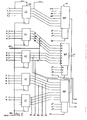
- Level Converters 100 also labeled LC, (quad BUS receivers, MC10129) are interfaced with a computer and particularly with the parallel output lines labeled 1 through 18 of the computer and provide a temporary latch storage of the data.
- serializing means 110 such as 3 eight-station Multiplexers (MC10164; within the box representing one of the Multiplexers are numbers illustrating specific pin connections as employed.)
- Serialized output from these Multiplexers in a sequence starting at the very top and terminating at the very bottom of the column of Multiplexers 110, passes out line 111 in Figure 2 and is incoming at line 111 of Figure 3 where it is delivered to a Phase Modulator 120 which may be of any suitable construction to enhance transmission--illustratively a dual Type D master-slave flip-flop 121 (MC10131), a quad OR/NOR Gate 122 (MC10101), and a triple 2-input exclusive-OR gate 123 (MC1672), in a known configuration for phase modulation.
- Phase Modulator 120 may be of any suitable construction to enhance transmission--illustratively a dual Type D master-slave flip-flop 121 (MC10131), a quad OR/NOR Gate 122 (MC10101), and a triple 2-input exclusive-OR gate 123 (MC1672)
- Modulated pulses pass then to a Driver 125 (MC10192) for differential transmission to the opposite or B end of my logic circuitry.
- a Driver 125 MC10192
- Any suitable Driver for sending the phase modulated pulses out through a conduit of any suitable type to the logic circuitry at the opposite end of the conduit may be employed.
- a conduit of coaxial cable is preferred. But even optical means such as fiber optics may be used, if desired. I favor differential transmission of parallel two lines each way for the comparative value inherent in the practice of differential transmission.
- the operation of the sending logic circuitry is controlled by clock pulses from a Crystal Clock CC 130 whose clock pulses may be generated in any suitable manner (not shown) and sent through the output lines shown from it.
- Clock line 132 (lower left of Figure 3) passes to Figure 4 where it continues as line 132 feeding clock pulses into a first bank of Registers 134, also labeled RGl, as well as a second bank of Registers 136, also labeled RG2.
- the uppermost registers of each of these banks may constitute master-slave flip-flops (MC10176), each containing 6-bit flip-flops with clocking being common to all 6 individual flip-flops.
- banks 134 and 136 each include two additional Registers, namely 134a and 134b and 136a and 136b.
- Each of these additional Registers suitably may consist of a dual master-slave Type D flip-flop (MC10131).
- Incoming lines 10L through 17L at the left of Figure 4 conduct samples of level converted output from lines of comparable number shown exiting from Figure 2.
- the sampled output of these lines is passed in parallel through each Register 134 and 136, with the data in Register 134 being one clock pulse behind that in Register 136.
- the sampling lines feed directly into the Register 134.
- line 12L which illustratively carries converted level of a "command" line from a computer
- line 16L which illustratively carries converted level of a "suppress” signal from a computer
- a special control box 137 and 138 respectively, each suitably consisting of a dual 2-wide 2-3-input OR- AND/OR AND-INVERT gate (MC10117).
- a Comparator CP suitably consisting of two gate units 140a and 140b, each suitably being a quad exclusive OR gate (MC10113). Outputs from each bank of Registers 134 and 136 are passed to the Comparator. Illustratively, lines exiting Register 134 labeled llR through 14R are shown to continue into the Comparator by the same labeling at inputs of the Comparator. Thus the signals of control (e.g. TAG) in the bank of Register 136 are compared against those in 134, which is one clock pulse behind the signals in Register 136. Where the data in the two Registers is the same, nothing occurs within the Comparator 140.
- TAG the signals of control
- the Comparator output 141 is that of a pulse of one clock width which is carried over and enters at OP at the middle left of Figure 5, marked as line 141.
- the same pulse of one clock width also travels out line 142.
- Gate 143 (a triple 2-3-2 input OR/NOR gate, MC10105) - - assuming that other circuitry of my logic does not dictate any mode other than Mode 1 - - allows it to pass through and set the flip-flop 144 (a master-slave flip-flop, MC10131) so as to provide a signal G024 at its lower or complement pin.
- the G024 signal from flip-flop 144 enters at 145 in Figure 3 and enters as G024 in Figure 6. Saving details of the circuitry of Figure 6 for later, the result of a G024 signal entering Figure 6, absent signals causing a different mode for transmission, is that of establishing at this point a Mode 1 transmission.
- the outputs Ml and M2 from the circuitry of Figure 6 enter the topmost Multiplexer in Figure 2 and dictate the mode condition to be transmitted to the receiver logic at the remote end of the transmission medium.
- the G024 signal entering line 145 of Figure 3 goes through logic which controls the Multiplexer operation in a manner that in fact causes the 24-bit transmission of Mode 1.
- a gate 146 (a triple 2-3-2 input OR/NOR gate, MC10105), having no contrary input, allows the G024 signal through. From that gate, it goes to two separate flip-flops 147 and 148 (each a dual type D master-slave flip-flop, MC10131). Also fed to these flip-flops 147 and 148 is the clock pulse coming from a like flip-flop 149 (MC10131) interposed in the line from clock 130.
- the input of half-clock time from flip-flop 149 is significant and perfectly times release of a signal for 24-bit operation from flip-flops 147 and 148 with the timed synchronization SYN. From flip-flop 148, the signal goes out line 102 as a Channel Latch CHLA signal to the line 102 of Figure 2 and prevents change of data while multiplexing and sending the message or byte.
- the signal triggers initiation of count by Counter 150 (a universal hexadecimal counter, MC10136) and counter means 151 (a dual Type D master-slave flip-flop, MC10131), both operating at crystal clock CC time.
- the LOGO input comes from like labeling in Figure 9 and is but a constant zero input.
- Outputs labeled 2 0 , 2 1 , and 2 of Counter 150 are fed into Multiplexer 110 in Figure 2 at the same respective labeling.
- Control of multiplexer propagation times is accomplished by signals OX, IX and 2X from translator shift gate 152 (a Dual Binary TO 1-4-DECODER, MC10171) responsively to counters 150 and 151 in Figure 3.
- the Synchronization Signals SYN from SYN in Figure 3, are constantly generated and go out the multiplexer to synchronize the entire logic at the receiving end during non-multiplexing times, that is non-message times.
- a translator gate 153 (Figure 3), also labeled TR (suitably a triple 2-3-2 input OR/NOR gate, MC 10105) senses the counts sent to the Multiplexers from the Counters 150 and 151.
- the receiver 200 ( Figure 9) is suitably a triple line receiver (MC10114), having one input connected to one line and a second input connected the second line of the coaxial cable, since differential transmission was employed in the illustrated case for greater accuracy and control.
- phase modulated data passes through a phase demodulator PD of conventional components and any suitable construction.
- the illustrated demodulator consists of OR/NOR gates 201, 202 and 203 (MC10101), exclusive OR gates 204 and 205 (MC1672), master-slave flip-flops 206 and 207 (MC10131), and a delay line with resistor 208.
- the function of the Phase Demodulator is simply to return the phase modulated data back to its condition before modulation.
- the illustrated demodulator also functions to separate the data and the clock signals when they are received in phase modulated form.
- the output of flip-flop 207 is that of non-return-to-zero data NRZ and the output of the OR/NOR gate 203 is that of the clock pulse CLP of data transmission.
- the NRZ data is immediately forwarded through Shift Registers 209 and 210, also labeled SR1 and SR2 (each a 4-bit universal Shift Register, MC10141), controlled by the clock signal from gate 203.
- the Shift Registers simply convert the serialized data coming in over the coaxial cable back to parallel outputs, which outputs are labeled A through F within circles in Figure 9. While two 4-bit Shift Registers are illustrated, only 6-bit capacity would be necessary under the particular conditions shown where the parallel output at this stage is 6 bits in parallel.
- the 1011 start output from the translator 212 sets a flip-flop 213 (master-slave, MC10131), also labeled GR, through the agency of a gate array 214 (a dual 4-5-input OR/NOR gate, MC10109).
- a gate array 214 a dual 4-5-input OR/NOR gate, MC10109.
- the flip-flop 213 puts out a signal GR, that is, "Go-Receive", which starts both counters 219 and 220 (universal hexadecimal counters, MC10136), with the input to Counter 219 coming from flip-flop 213.
- the input to Counter 219 sets gate 215 (triple 2-3-2 input OR/NOR gate, MC10105).
- the output from the counters is that of counts equalling 3, 6, 12, 18, and 24 as shown at the right in Figure 9. How this is accomplished is as follows: Counter 219 only initiates the count and only counts to 6; at which time an OR/NOR gate 221 (MC10105) resets counter 219 and steps counter 220, which counts in increments of six thereafter.
- the gate 222 (dual 4-5 input OR/NOR, MC10109) responds at the count of 3 to send out an equal 3 signal which causes sampling of outputs circle E and circle F from the Shift Register 209.
- the sample outputs at circle E and circle F will be noted, at the count of equal 3, to contain the two mode bits, Ml and M2 as transmitted. They will be noted to enter the logic circuit of Figure 10 at the left, where the labels circle E and circle F are found. That circuit will be explained below.
- a decoder 224 (dual binary TO 1-4 decoder, MC10171) is interposed and passes output to a quad OR/NOR gate 226 (MC10101) which provides a sequence of count outputs at equal 6, then equal 12, then equal 18, and finally equal 24.
- MC10101 quad OR/NOR gate 226
- MS a quad 2-input multiplexer/latch, MC10173
- a 24-bit Shift Register need not be used, and that the counts of 6, 12, 18, and 24 from the quad OR/NOR gate 226 are used to control the filling of four 6-bit Main Registers 240, 241, 242, and 243, all also labeled as a first bank Buffer Register BR1 (each being a Hex "D" master-slave flip-flop, MC10176).
- the first 6 bits of a received data byte fill Register 240, and then Registers 241, 242, and 243 are filled with the remaining 24-bit Mode 1 transmission (shifting to each in sequence according to the count input setting).
- the first 9 bits (after the internal first 3) pass through switches SW into the bank of receive level converters 250 (each being bus driver, MC10128), where they are converted back to levels understood by the peripheral device and made ready for feed out to the peripheral device on lines 1 through 9 at the right in Figure 11.
- the bits going out lines labeled A10 and Bll and C12 of register 242 (which illustratively represent service, data, and command signals from the computer, which are transmitted as "bits" and received here) are preferably handled somewhat differently, for reasons which will be evident below.
- MS a quad 2-input multiplexer/latch
- MC10173 a quad 2-input multiplexer/latch
- Those signals A10 and Bll leave selector 234 as MS and MD and enter switch 247 ( Figure 11). In Mode 1, they go directly through switch 247 and are converted by the level converter RLC for lines 10 and 11 to the peripheral device.
- the "command" signal of line C12 from register 242 of Figure 11 is passed directly to C12 of the gate 249 of Figure 11 (a dual 2-wide 2-3-input "OR-AND/OR-AND-INVERT”gate; MC10117). With no contrary input to that gate in Mode 1, the C12 signal passes to the Receive Level Converter and out line 12. Remaining outgoing lines of registers 242 and 243 go directly to the level converter RLC for conversion.
- lines A10, Bll, and C12 of register 242 could go directly to the level converter RLC in Mode 1, but they are preferably handled as aforenoted inasmuch as the bits or signals (e.g., service, data, and command) carried by those lines are not part of the smaller message transmissions in other modes and yet are important for some types of equipment serviced by my logic circuitry and important for special purposes in Modes 2 and 3, as will be explained. Thus even in Mode 1, I control those signals, as illustrated.
- the only significant action of the signal RR ( Figure 10) is that of passing through gate 255 (a dual 2-wide 2-3-Input OR-AND/OR-AND-INVERT gate, MC10117) to a controller or multiplex selector 256 (Quad 2-input multiplexer/latch, MC10173), and then out on line 257 as a gate channel signal GCH which enters Figure 11 at line 257 to effectively allow passage of all parallel bits simultaneously to the level converters RLC and out to the peripheral unit.
- gate 255 a dual 2-wide 2-3-Input OR-AND/OR-AND-INVERT gate, MC10117
- controller or multiplex selector 256 Quad 2-input multiplexer/latch, MC10173
- OR/NOR gate 260 (suitably a Quad OR/NOR gate, MC10101).
- the first and third inputs namely RM3 and RM2, pass selector 320; and to be especially noted is that these pass to gate 252 to cause an RR output for the A end at the counts of 12 and 6, respectively, both of which can be relevant for A end receipt of transmissions from the B end.
- two other OR/NOR gates 262 and 264 are also at the left in Figure 9 (each MC10101).
- Gate 262 controls the input of the Master Clear signal aforementioned.
- Gate 264 controls the condition for the logical zero connections, i.e., the LOGO condition.
- the response from an external peripheral unit back to the computer is communicated in the same manner as that hereinabove described for a communication from the computer to the peripheral.
- the sending circuitry of Figures 2, 3, 4 and 6 is present in my logic circuitry at the peripheral end and used by it to send a Mode 1 acknowledgment of 24 bits; and the receiving circuitry of Figures 9, 10 and 11 is present at the computer end and used to receive from the periphery.
- the bits of the periphery's acknowledgment back to the computer may carry different significance (e.g. instead of service and data "out” bits, the periphery's acknowledgment may be that of service and data "in” bits or signals for input to a computer, etc.).
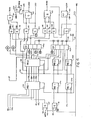
- Mode 2 the WRITE mode of transmission.
- the messages through my logic are sent only on the significant edge (leading or trailing) of service or data signals; and the significant edge of those signals varies depending on whether the A or B end is sending and whether the Mode is 2 or 3.
- Gates 180, 181, 182, 183 are AND gates (Quad 2-input AND, MC10104) for establishing a signal as labeled just to their right, namely TES, TED, LES and LED. Their input lines are shown; and it should be recognized that line 10L sampling is that of "service” and line 11L sampling is that of "data..
- Gates 184 and 185 are OR/NOR gates (triple 2-3-2 input, MC10105), with their output being that of TESD and LESD, respectively. In Mode 2 transmission, the LESD signal from Figure 4 enters at LESD in Figure 3.
- Gates 186, 187, and 188 in Figure 4 are Quad OR/NOR gates (MC10101), with signals relevant to service and data exiting the Comparator 140 going to gates 186 and 187 respectively.
- a gate 189 (dual 2-wide 2-3 Input "OR-AND/OR-AND-INVERT, MC10117) receives input from OR/NOR gate 188, which in turn is fed from line 301.
- the group of gates 186 through 189 controls the signal to gate 143 in a manner that, once a Mode 2 or Mode 3 condition is signaled from line 301, the resulting signal from gate 189 to OR/NOR gate 143 places gate 143 in a blocking or NOR position preventing any 24 bit transmission until the Mode 2 or 3 transmission is completed.
- Mode 2 (or Mode 3) from Mode 1 involves special circuitry in Figure 5.
- data bits for reading and writing and command are sampled after level conversion and before serialization.
- the lines marked DA through DE ( Figure 2) are sampled and the bundle of lines 104 for sampling connects with the lines of input marked respectively DA through DE in Figure 5.
- lines DA through DD carry data bits 6, 7, 4 and 5, respectively, bearing on instructions for read, read backwards, write, etc.
- line DE carries command signals.
- the sample lines DA through DE feed an array of gates as follows: OR/NOR gates 160, 161 and 162 (Quad OR/NOR, MC10101); OR/NOR gates 163, 164, 165 (dual 4-5 input OR/NOR, MC10109); and AND gates 166 and 167 (Quad 2-input AND, MC10104).
- the setting and gaining of the output signals is accomplished by a few steps, which will be illustrated as basically four.
- the steps may vary depending on the nature of external devices employed.
- a computer and peripheral may be exchanging random messages in Mode 1 and the computer may advise the peripheral that it has something which causes the peripheral to advise the computer that it has raised its "address in”.
- the computer responds with "command out” and other pertinent instruction signals (leading toward read or write) which on sampling into Figure 5 enter the first flip-flop in the series of four. Since the same steps are involved for establishing either a READ or WRITE condition, description of a WRITE condition is sufficient. Thus, the pulse enters WRT1 on the rise of the signal "command out".
- the response of the peripheral is a drop of address in; and the computer communicates back that it drops “command out”, which on sampling in Figure 5 is a “fall or drop of "command out” in flip-flop WRT2.
- the computer communicates "service out”, which is a rise or change entering WRT3.
- the peripheral responds dropping "status in”
- the computer communicates its fourth and last message in the process of establishing a Mode 2 (or Mode 3) condition. This fourth message from the computer at this phase is one which effectively is a fall of "service out” in flip-flop WRT4, which generates the Mode 2 output WRT4 in Figure 5.
- the comparator pulse entering line 141 of Figure 5 passes through gates 178 (MC10105) and 176 (MC10101), which delays the pulse until after the aforenoted clear action of it; and this delayed pulse sets or enables, as a clock input, the first and second flip-flops in each group of four. Recognize that once the command line signal of line 12L entering Figure 4 has performed its function at the comparator and for the first two flip-flops of each group of four in Figure 5, there should no longer be any comparator pulse out line 141.
- the SODO signal sets the clock input of the flip-flops RED3, RED4, WRT3, and WRT4, and by delay through gates 178 and 176 does the same for the first two flip-flops of each group; but the sequence of signals effectively accomplishes movement of the instruction pulses through the four flip-flops for establishing a Mode 2 (or 3) condition.
- Figure 5 shows an output signifying "false" WRT 4, or not write four (NWRT4). That output is a significant input signal for the circuitry of Figure 6, where Mode per se is established.
- the input of NWRT4 in Figure 6 forces a Mode 2 despite the fact that G024 is true and a 24 bit message is being sent. This is significant for that last or fourth communication from the computer to the peripheral in establishing a change of mode. It allows that last communication to be in full multiplexing, despite the introductory Mode instruction for Mode 2.
- a mode discriminator 190 receives its input directives from lines at its left. In tracing Mode 2 happenings, the relevant inputs are the NWRT4 and WRT4 inputs just mentioned. Output from the discriminator goes to a Quad AND gate 191 (a Quad 2-input AND, MC10104); and its output is that of the mode lines M1 and M2 feeding the multiplexer 110 of Figure 2.
- the B end adjacent an external peripheral receives the mode change messages and sends replies back to the A end in Mode 1 (i.e., 24 bits and G024), except for the reply to the fourth and last mode change message from the A end where the leading bits establish a Mode 2 condition despite the 24 bits employed for that transmission.
- Mode 1 i.e., 24 bits and G024
- the mode bits of that fourth transmission would normally be expected to cause the receiving Figure 9 circuitry at the B end to limit the count to 12; but I prevent that even though received message counts thereafter in Mode 2 are limited to 12.
- the signal BM 2 thus generated enters Figure 7, passes gate 340 (MC10101), sets flip-flop 342 (MC10131), and enters flip-flop 344 (MC10131) to cause the generation of a G06 output.
- the A end uses solely the mode bits of it to create for the computer an acknowledgment input that causes the computer to believe that the peripheral device itself has sent a "service in” message, even though the message is not one from the peripheral device.
- the A end does that by using the RM2 output from the A end decoder 232 ( Figure 10), which enters the A end multiplexer switch 320 ( Figure 9), passes to gate 252 and exits as RR at the count of 6 at the A end.
- the A end circuitry of Figure 8 is employed, with the RM2 signal entering flip-flop 366 (MC10131) and gate 370 (MC10105), and RR entering flip-flop 366 on clock.
- the resulting signal from gate 370 goes to flip-flop 362 (MC10131) and out as an SI signal. That signal SI enters the multiplex switch 352 (MC10173) at the A end Figure 10 circuitry, which emits a signal to selector switch 234 at the A end.
- the result at the A end is that the output MS of switch 234 is actually a "modified service in", which enters switch 247 of Figure 11 and passes to the computer, where it is received and interpreted as "service in” response from the peripheral.
- the M2 line of Figure 6 is connected to the M2 line in Figure 4, effectively causing a NOR condition for gate 143 and effectively blocking any "suppress" bits on line 16L from passing gate 138.
- the WRT4 signal entering Figure 4 from Figure .5 similarly blocks any "command" bits on line 12L from passing gate 137, for so long as the Mode 2 (or Mode 3) condition is maintained. (In Mode 3, the WRT4 input would be RED 4.)
- the LESD is an activator to cause the G012 signal for each Mode 2 transmission.
- the significance of LESD may be taken as "Leading Edge of Service Out Data Out.”
- this circuit there is an OR/NOR gate 193 (MC10105), another OR/NOR gate 194 (MC10101), and a flip-flop 195 (MC10131) from which two signals exit, namely a WRT6 and G012.
- the G012 goes to the input of identical marking in Figure 3.
- the G012 in Figure 3 initiates the transmission in a manner comparable to that described for the G024 transmission, except that transmission in Mode 2 is limited to 12 bits per message.
- the WRT4 (from Figure 5) with clock release by LESD (from Figure 4) goes to flip-flop 196 (MC10131) of Figure 3.
- Flip-flops 148 and 196 in Figure 3 suitably may function on an "or" basis for the channel latch signal of line 102.
- the WRT6 output in Figure 3 could, for high or highest speed transmission, be the input replacing the constant enabling WRT4 to flip-flop 196, if desired.)
- the signal RM2X enters Figure 9 in a multiplex switch 320 (MC10173). It sets that switch and effectively thereafter limits the count to 12 bits for so long as Mode 2 is maintained at the B end.
- a signal goes out line 253 to Go Receive 213 to stop the Receive Counter 220.
- the RR signal from gate 252 is generated.
- This signal BM2, apart from its function earlier mentioned, enters Figure 11 as the signal controlling the switches 245, 246 and 247, effectively causing subsequent data of Mode 2 (12 bits) to enter the buffer registers (all MC10176) instead of allowing subsequent Mode 2 data (after the special 24 bit mode setting communication) to by-pass the buffer registers.
- the signal RM2X from flip-flop 311 goes to Figure 11 and enters the lower second set buffer register BR2. (The RM2X of each Mode 2 receipt does this.)
- control for shifting all 12 bit WRITE data through the buffer registers of BR1 through BR12 of Figure 11 is initiated. How this is done requires reminder that the entire circuitry is present at both ends.
- the control or recognition at the A end as to the availability of buffer space at the B end is best understood after knowledge of what is happening as WRITE mode "bytes" (of 12 bits) are received at the B end.
- All flip-flops Fl through F12 are master-slave (MC10131); all gates G2 through G12 are triple input OR/NOR (MC10105) and all return gates marked ON are Quad OR/NOR (MC10101). What happens is that the X and Y signals at the B end set Fl to indicate register BR1 is full. But if BR2 is empty and BR1 full, a pulse is generated which causes gate G2 to open the Buffer Register BR2 for data from BR1 to move into it, or shift or transfer data from BRl to BR2. This simultaneously causes clearance of flip-flop Fl to indicate that buffer register BR1 is capable of receiving data and sets F2 indicating BR2 is full.
- the signal from G2, opening BR2 for data, also sets master-slave flip-flop F2 on clock causing G3 to permit the data to shift from BR2 into BR3 (if empty) and clear F2, etc., until the initial data is transferred into Buffer Register BR12, at which time a pulse from G12 sets F12 to indicate that the data has entered BR12 and that BR12 is full.
- the A end circuitry of Figure 11 is, to a limited extent, duplicating the B end.
- the output X and Y at the A end enters Fl flip-flop 331 (Fig. ll) at the A end and goes through the flip-flops Fl through F12, essentially duplicating their action at the B end, but without data in the A end buffer registers (which may be omitted, if desired). This is done at the A end solely for the purpose of keeping track of buffer register available space at the receiving end, for reasons which will be evident below.
- gates 314 and 315 as well as 255 are all OR-AND/OR-AND INVERT (Dual 2-wide 2-3-Input, MC10117).
- Gates 316 and 317 are OR/NOR gates (Quad, MC10101).
- Flip-flops 228, 313, 318 and 319 are dual type B master-slave flip-flops (MC10131).
- the multiplexer switches or selectors 234, 350 and 352 are all Quad 2-Input multiplexer latches (MC10173).
- gate 334 is an OR/NOR gate (MC10105); gate 335 is also OR/NOR (MC10101); and flip-flop 336 is master-slave (MC10131).
- the pulse from G12 passes an ON gate to set F12, but not on clock, and passes through gates 334 and 335 to set flip-flop 336, which may be considered the thirteenth in the flip-flop series.
- Flip-flops F12 and 336 remain set until the action by the peripheral device causes them to be cleared, as follows:
- a "service in" request for a byte by the peripheral enters LESD. (Recognize, as will be evident, that both the leading edge and trailing edge of service or data are significant signals for the B end operation adjacent the peripheral device.)
- the LESD enters the flip-flop 336 and clears it by clocking ground into it.
- the output MSB from flip-flop 318 is effectively a "service out” signal for the peripheral.
- the peripheral made a request by "data in”, effective response to it as “data out” would be generated as MDB in flip-flip 319, in a manner comparable to that of the service request.
- the "service out” together with the data in BR12 are gated as aforenoted and accepted into the peripheral; and the peripheral acknowledges by dropping its "service in”, which causes a TESD operation in the B end circuitry of Figure 4. (Remember that the sending circuitry discussed above is not just interfaced with the computer, but also the peripheral.)
- the RM2X signal from flip-flop 311 of Figure 10 passes with the byte through the buffer registers and exits BR12 as RM2Y.
- the signal RM2Y enters Figure 10 at flip-flop 313.
- the RM2Y of each byte sets flip-flip 313; and G13 off gate 334 then clocks it out or clears flip-flop 313 of the RM2Y for the byte at the time the peripheral empties or takes the byte from BR12.
- the pulse G13 from gate 334 in Figure 11 clears flip-flop 313 and that flip-flop is left clear when the buffers are clear of data.
- a computer adjacent the A end may well finish its WRITE to a peripheral before all bytes of Mode 2 have been removed from the buffer registers by the peripheral.
- the computer may signify its completion by raising "command out", which will effectively remove the A end from Mode 2 into Mode 1 and generate a 24 bit transmission to the B end. This could put the B end in danger of losing data but for the aforenoted control of its Mode 2 condition until it empties the buffer registers. But even that control can be dominated by a computer command; and to prevent that occurrence, the command line C12 in buffer 242 is connected to gate 249 (MC10117) in Figure 11 instead of directly to a receive level converter RLC.
- the second important event is that of generating an acknowledgment back to the A end.
- the acknowledgment is one of only 6 bits, as aforenoted, but is generated differently from the first "service in" acknowledgment.
- the control circuitry of Fl through F12 in Figure 11 is at least duplicated at the A end.
- the gating to and sequential setting and clearing of flip-flops at the A end takes place through to F12, with flip-flops F12 and those behind it set in parallel with flip-flops of the same designation at B.
- An Fl output (signifying clear) from flip-flop 331 at the A end is required as an input to gate 193 of Figure 5 to enable that gate before the A end will send a G012 signal for a WRITE message to the B end.
- the LESD from Figure 4 for each WRITE message the computer is about to send is a clocking input to flip-flop 192 for that sending circuit; but availability of buffer register space by the Fl input is required before a transmission of G012 is ordered.
- the RR signal so generated enters the A end selector 350 of Figure 10 which also has the WRT4 input of the A end.
- the availability of buffer space at B is monitored at the A end and permits great time saving.
- Transmission from A to B and vice versa can take place simultaneously since different lines are preferably employed; and each end contains logic used to maintain operation of the external devices by converting their own signals into ones each "believes" is from the other.
- flip-flop 360 To satisfy an external computer's requirement for a "service in” or “data in” communication (as from a peripheral unit) before a byte is released by it, I employ a special circuit illustrated in Figure 8 to generate response to the computer from the computer's own output.
- the circuit consists of flip-flops 360, 362 and 364 (MC10131) and a gate 368 (MC10117).
- Flip-flop 360 is equipped with a circuit shown in the drawing as having a conventional switch (left open in the drawing). In the condition shown in the drawing, but with the switch closed, flip-flop 360 toggles between service and data, that is, causes the output of SI and DI, as shown at the right in Figure 8.
- Figure 8 circuitry is specialized and adjustable to provide whatever return signal is needed to satisfy the demands of an external computer for continued release of bytes or messages.
- the circuit generates the return signal using the computer's output, which initiates action by my A end sending circuitry.
- the arrangement permits a computer to send WRITE message bytes as fast as it can, limited only by the availability of buffer receipt. In this respect, more buffers than illustrated (or less) may be employed.
- Gates 314 and 315 ( Figure 10) for channel latch at the A end are not necessary.
- the channel latch at the A end is essentially wide open at the A end in both Mode 2 and Mode 3.
- Most computers are capable of greater speed than peripheral devices.
- the line from the upper mode bit just before decoder 232 and extending to gate 255 is a line which always carries bits indicating either Mode 2 or Mode 3, controlling passage at gate 255 (MC10117).
- Mode 3 operation will normally be established at the end of my logic adjacent a computer.
- the steps are analogous to those for establishing Mode 2, as discussed above and illustrated in Figure 5.
- mode 3 at the "fall" of service establishing it, where RED4 input is made in the mode setting circuit of Figure 6, the B end's receipt of the 24 "bit” establishing transmission is held by flip-flop 228 ( Figure 10) in a manner analogous to that explained for flip-flop 311 for Mode 2.
- received messages of Mode 3 are processed through the circuit of Figure 9, with selector input RM3 (from Figure 10) setting the 12 count.
- Figure 12 shows replacement circuitry for the lower left of Figure 4.
- the Figure 12 circuitry is very effective in stopping a computer's suppress signal of line 16L from propagating into the first bank registers RG1 when the transition is taking place to a Mode 2 condition.
- the circuitry of Figure 4 is also effective to do so, but only when or after WRT4 from Figure 5 has been set to cause an M2 signal.
- Figure 12 circuitry is an improvement in that it is effective to stop a suppress in line 16L at any stage during the transition to the WRITE or READ condition.
- Figure 12 circuitry at the A end, has a gate 410 (dual 2-wide 2-3-input "OR-AND/OR-AND-INVERT", MC10117) whose inputs labeled REDl through RED4 inclusive and WRT1 through WRT4 inclusive are from the respective outputs of like labeling in Figure 5. All output from the gate goes through line 411 to a clock input of flip-flop 413 (a dual type D master-slave flip-flop, MC10131). Recognize also that the flip-flop receives clocking input from line 132; and that line also carries clocking for the shift through the registers RG1 and RG2 to the comparator as shown in Figure 4. Further at the A end, the output of gate 138 is passed to the flip-flop 413.
- flip-flop 413 a dual type D master-slave flip-flop
- the arrangement of the Figure 12 circuitry at the B end or B box employs a peripherals incoming signal on line 17L to pre-set flip-flop 413.
- This forces any "request in” entering line 16L from any peripheral into a false condition, a feature especially desirable when multiple peripherals are serviced at the B end.
- an "operational in” signal of line 17L prevents any "request in” on 16L from passage through the flip-flop 413. This is especially important where two different peripherals are serviced by the B box circuitry.
- the "operational in” peripheral is effectively the controlling peripheral to stop any "request in” signal from the other.
- Figure 12 circuitry is to not only stop any "request in” from generating a G024 signal, but also to make sure that the computer at the other end or A end does not see any "request in”. That feature is effectively accomplished by forcing any "request in” to zero.
- line 16 Figure 2 after leaving the level converter labeled LC is broken or removed between the joining of 16L to it and the multiplexer 110.
- line 414 is fed as a substitute line 16 to the multiplexer 110 at the B end, with the result that any "request in” signal on line 16L by any alternate peripheral is fed through as a zero.
- a still further improvement in the circuitry of Figure 8 for the A end is that of a substitution of trailing edge of service or data, TESD, for the WRT6 input to gate 368.
- the TESD input comes from the output of like labeling in Figure 4, and is generated at the A end as the Mode 2 messages are sent for filling the buffer registers at the B end.
- This improvement slightly slows down the "service in” or SI response generated by the Figure 8 circuit for sending back to the computer.
- the WRT6 input to gate 368 tends to cause the SI to occur too fast and allows the computer to change data in some instances.
- the noted improvement does not allow the sending of the next "service in” until the transition or "service out” drop.
- the fragmentarily delayed "service in” signal accomplished by employing TESD instead of WRT6 as an input to gate 368 slows response to the computer sufficiently so that there is no improvident change of data for any single byte.
- the added circuitry option there illustrated for the upper left of Figure 10 contributes to a forcing of a preset of Mode 2 condition in flip-flop 313 at the beginning of Mode 2 or the WRITE condition.
- gates 430, 431, and 432 are all triple 2-3-2 input OR/NOR gates (MC10105); and flip-flop 433 is a dual type D master-slave flip-flop (MC10131).
- BM2 functions to block passage of a line C12 signal in Mode 2.
- the ST will set flip-flop 433. That setting combined with gate 431 will effectively continue to prevent any incoming C12 signal (such as Command Out) from going to the peripheral during Mode 2.
- flip-flop 433 Once flip-flop 433 is set, it will only clear on Mode 1, on the RR input to gate 432 after that gate receives input of RM1, and absence of Command Out.
Landscapes
- Engineering & Computer Science (AREA)
- Theoretical Computer Science (AREA)
- Computer Networks & Wireless Communication (AREA)
- Signal Processing (AREA)
- Physics & Mathematics (AREA)
- General Engineering & Computer Science (AREA)
- General Physics & Mathematics (AREA)
- Power Engineering (AREA)
- Communication Control (AREA)
- Time-Division Multiplex Systems (AREA)
- Information Transfer Systems (AREA)
Applications Claiming Priority (2)
| Application Number | Priority Date | Filing Date | Title |
|---|---|---|---|
| US48642783A | 1983-04-18 | 1983-04-18 | |
| US486427 | 1983-04-18 |
Publications (2)
| Publication Number | Publication Date |
|---|---|
| EP0122870A2 true EP0122870A2 (fr) | 1984-10-24 |
| EP0122870A3 EP0122870A3 (fr) | 1987-06-24 |
Family
ID=23931846
Family Applications (1)
| Application Number | Title | Priority Date | Filing Date |
|---|---|---|---|
| EP84630061A Withdrawn EP0122870A3 (fr) | 1983-04-18 | 1984-04-17 | Système de transmission de données à portée étendue |
Country Status (4)
| Country | Link |
|---|---|
| EP (1) | EP0122870A3 (fr) |
| JP (1) | JPS60501088A (fr) |
| CA (1) | CA1276309C (fr) |
| WO (1) | WO1984004220A1 (fr) |
Cited By (1)
| Publication number | Priority date | Publication date | Assignee | Title |
|---|---|---|---|---|
| EP0401803A3 (fr) * | 1989-06-06 | 1992-01-22 | Comtrol Corporation | Multiplicité de postes de travail graphique à distance |
Family Cites Families (11)
| Publication number | Priority date | Publication date | Assignee | Title |
|---|---|---|---|---|
| US3909526A (en) * | 1972-04-20 | 1975-09-30 | Mi 2 74245 76919720420013 781 | Square wave oscillator for a data terminal |
| US4205200A (en) * | 1977-10-04 | 1980-05-27 | Ncr Corporation | Digital communications system utilizing controllable field size |
| US4187394A (en) * | 1978-04-25 | 1980-02-05 | The United States Of America As Represented By The Administrator Of The National Aeronautics And Space Administration | High-speed data link for moderate distances and noisy environments |
| JPS5698051A (en) * | 1980-01-07 | 1981-08-07 | Hitachi Ltd | Signal transmitting device of lsi component |
| FR2475827B1 (fr) * | 1980-02-13 | 1987-05-29 | Dauphin Jean Louis | Systeme de commutation numerique a division du temps pour voies mic vehiculant la parole et des donnees en mode-paquet |
| FR2476880A1 (fr) * | 1980-02-27 | 1981-08-28 | Ibm France | Procede et dispositif pour multiplexer un signal de donnees et plusieurs signaux secondaires, procede et dispositif de demultiplexage associes, et emetteur-recepteur d'interface en faisant application |
| US4325147A (en) * | 1980-06-16 | 1982-04-13 | Minnesota Mining & Manufacturing Co. | Asynchronous multiplex system |
| DE3068177D1 (en) * | 1980-06-19 | 1984-07-19 | Ibm | Flow control mechanism for block switching nodes |
| JPS57173255A (en) * | 1981-04-17 | 1982-10-25 | Mitsubishi Electric Corp | Facsimile transmitter |
| US4423414A (en) * | 1981-08-27 | 1983-12-27 | Burroughs Corporation | System and method for name-lookup in a local area network data communication system |
| JPS5859665A (ja) * | 1981-10-05 | 1983-04-08 | Mitsubishi Electric Corp | 書画伝送装置 |
-
1984
- 1984-04-16 CA CA000452086A patent/CA1276309C/fr not_active Expired - Lifetime
- 1984-04-16 JP JP59501835A patent/JPS60501088A/ja active Pending
- 1984-04-16 WO PCT/US1984/000567 patent/WO1984004220A1/fr not_active Ceased
- 1984-04-17 EP EP84630061A patent/EP0122870A3/fr not_active Withdrawn
Cited By (1)
| Publication number | Priority date | Publication date | Assignee | Title |
|---|---|---|---|---|
| EP0401803A3 (fr) * | 1989-06-06 | 1992-01-22 | Comtrol Corporation | Multiplicité de postes de travail graphique à distance |
Also Published As
| Publication number | Publication date |
|---|---|
| JPS60501088A (ja) | 1985-07-11 |
| CA1276309C (fr) | 1990-11-13 |
| EP0122870A3 (fr) | 1987-06-24 |
| WO1984004220A1 (fr) | 1984-10-25 |
Similar Documents
| Publication | Publication Date | Title |
|---|---|---|
| US4314367A (en) | Switching circuit for digital packet switching network | |
| EP0186420B1 (fr) | Systèmes de communication de données | |
| US4264954A (en) | Distributed function communication system for remote devices | |
| US4542380A (en) | Method and apparatus for graceful preemption on a digital communications link | |
| US20020112099A1 (en) | Method and apparatus for deskewing multiple incoming signals | |
| US5748684A (en) | Resynchronization of a synchronous serial interface | |
| JPH0241221B2 (fr) | ||
| US4797951A (en) | Parallel optical data transmission system | |
| US5524218A (en) | Dedicated point to point fiber optic interface | |
| EP0225024A2 (fr) | Système de transmission de données | |
| US4430702A (en) | Network access device | |
| EP0692117B1 (fr) | Systeme de fusion de donnees paralleles a ultra-haute vitesse | |
| US4642629A (en) | Enhanced distance data transmission system | |
| US4823305A (en) | Serial data direct memory access system | |
| EP0498359A2 (fr) | Station pour bus annulaire avec deux oscillateurs | |
| US4746918A (en) | Split bus system interface | |
| AU596459B2 (en) | Data transfer system having transfer discrimination circuit | |
| USRE33404E (en) | Enhanced distance data transmission system | |
| EP0122870A2 (fr) | Système de transmission de données à portée étendue | |
| US4612541A (en) | Data transmission system having high-speed transmission procedures | |
| US4787025A (en) | Remote fan out facility for data terminals | |
| JPH0143499B2 (fr) | ||
| EP0241622B1 (fr) | Méthode de transmission efficace intégrant les données et l'information non codée | |
| CA1170739A (fr) | Dispositif d'acces a un reseau | |
| US4959843A (en) | Content induced transaction overlap (CITO) block transmitter |
Legal Events
| Date | Code | Title | Description |
|---|---|---|---|
| PUAI | Public reference made under article 153(3) epc to a published international application that has entered the european phase |
Free format text: ORIGINAL CODE: 0009012 |
|
| AK | Designated contracting states |
Designated state(s): AT BE CH DE FR GB IT LI LU NL SE Kind code of ref document: A2 Designated state(s): AT BE CH DE FR GB IT LI LU NL SE |
|
| PUAL | Search report despatched |
Free format text: ORIGINAL CODE: 0009013 |
|
| AK | Designated contracting states |
Kind code of ref document: A3 Designated state(s): AT BE CH DE FR GB IT LI LU NL SE |
|
| 17P | Request for examination filed |
Effective date: 19871210 |
|
| 17Q | First examination report despatched |
Effective date: 19890915 |
|
| RAP1 | Party data changed (applicant data changed or rights of an application transferred) |
Owner name: MEGABIT COMMUNICATIONS, INC. |
|
| RIN1 | Information on inventor provided before grant (corrected) |
Inventor name: MILLIGAN, JAMES H. |
|
| STAA | Information on the status of an ep patent application or granted ep patent |
Free format text: STATUS: THE APPLICATION IS DEEMED TO BE WITHDRAWN |
|
| 18D | Application deemed to be withdrawn |
Effective date: 19921103 |