EP0123376A2 - Connecteur utilisant un élément en alliage à mémoire de forme - Google Patents
Connecteur utilisant un élément en alliage à mémoire de forme Download PDFInfo
- Publication number
- EP0123376A2 EP0123376A2 EP84300718A EP84300718A EP0123376A2 EP 0123376 A2 EP0123376 A2 EP 0123376A2 EP 84300718 A EP84300718 A EP 84300718A EP 84300718 A EP84300718 A EP 84300718A EP 0123376 A2 EP0123376 A2 EP 0123376A2
- Authority
- EP
- European Patent Office
- Prior art keywords
- pin
- connecter
- shape memory
- memory alloy
- sheets
- Prior art date
- Legal status (The legal status is an assumption and is not a legal conclusion. Google has not performed a legal analysis and makes no representation as to the accuracy of the status listed.)
- Withdrawn
Links
Images


Classifications
-
- H—ELECTRICITY
- H01—ELECTRIC ELEMENTS
- H01R—ELECTRICALLY-CONDUCTIVE CONNECTIONS; STRUCTURAL ASSOCIATIONS OF A PLURALITY OF MUTUALLY-INSULATED ELECTRICAL CONNECTING ELEMENTS; COUPLING DEVICES; CURRENT COLLECTORS
- H01R4/00—Electrically-conductive connections between two or more conductive members in direct contact, i.e. touching one another; Means for effecting or maintaining such contact; Electrically-conductive connections having two or more spaced connecting locations for conductors and using contact members penetrating insulation
- H01R4/01—Connections using shape memory materials, e.g. shape memory metal
Definitions
- the present invention relates to a connecter suitable for transmitting electric signals between electronic circuit devices.
- a connecter using a shape memory alloy is disclosed in e.g. Japanese Patent Laid-Open No.16056/1973 entitled "Low Temperature Physical Connection Method and Device".
- This connecter establishes electric connection by making use of the recovery of shape of a shape memory alloy resulting from a martensitic reverse transformation due to a temperature rise.
- the shape memory alloy returns to its initial state by making use of the softness of the martensite phase generated by a temperature drop and by the restoring force of a spring.
- the connecter utilizes a one-way shape memory effect resulting in a large deformation and combines a shape memory alloy with a spring so as to cause effective two-way deformation.
- the prior art device is satisfactory if the size of the connecter is large.
- the present invention seeks to provide a connecter in which the problem of the prior art connecter discussed above is resolved by making possible the omission of the spring. It does this by providing a connecter with a connection terminal in the form of a thin sheet of shape memory alloy on a substrate.
- the connection terminal is adapted to receive a pin, thereby establishing an electrical connection.
- connection and disconnection may be made small relative to those necessary in the prior art connecter.
- present invention permits the connecter itself to be made small relative to the prior art connecter, making it particularly suitable for use where a compact connecter is required such as in an electronic computer.
- shape memory alloy is used for those alloys such as Ti-Ni, Ag-Cd and Cu-Al-Ni, which exhibit a memory effect.
- Marttensite phase hereinafter referred to as the "M phase”
- M phase thermoelastic martensite transformation
- the stress occurring at the time of reverse transformation from the M phase to the parent phase may be as great as 60 to 70 kg/ mm 2 .
- the parent phase has a shape denoted by A, for example, which shape is memorized at high temperatures and the material is then deformed to another shape denoted by B, for example, within the temperature range corresponding to the parent phase. Then the material does not return to its original shape memorized in the parent phase, that is, A, but remains in shape B even if the material is held in shape B whilst the temperature is reduced to a temperature range corresponding to the M phase and then the material is released.
- A shape denoted by A
- B for example, within the temperature range corresponding to the parent phase.
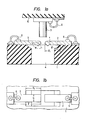
- the connecter shown in Figs. la and lb is formed by utilizing the properties of a shape memory alloy as described above.
- a metal film (not shown) is formed by sputter vapor deposition at a predetermined position on a heat- resistant oxidation-resistant flat insulator substrate 1 consisting of e.g. SiO 2 , or Al 2 O 3 .
- the thin sheet of shape memory alloy is then spot-welded onto the metal film. It is also possible to deposit the shape memory alloy film directly on the substrate by vapour deposition.
- the alloy film 2 thus formed is etched to a desired pattern, with a cross-sectional shape of the parent phase as shown in Fig. la, thereby forming a socket 4 of the connecter.
- Fig. lb shows a plan view of the socket 4 shown in Fig. la.
- Also shown in Fig. 1, are a pin 3 of a plug to be inserted into the socket, a fitting plate 5 and wire bonding 6 which connects the connecter to circuit wiring (not shown).
- the pin 3 of a plug (portions other than the pin are omitted for simplicity) is inserted into the hole of the socket 4 at a temperature substantially equal to the upper temperature limit of martensite transformation Ms or a temperature close to the upper limit of the temperature range, at which the M phase is stable, and which is lower than the former point. Then, the thin sheet 2 of shape memory alloy forming the socket 4 is pushed by the pin 3 and undergoes deformation as shown in Fig. 2b. However, the inserting force of the pin 3 in this instance is approximately 4 g, i.e. is not very large.
- the temperature of the connecter is reduced to a point lower than the lower temperature limit of martensite transformation Mf and the pin 3 is removed from the socket 4, as shown in Fig. 2d the connecter being maintained at that temperature.
- the pin 3 may be removed from the socket 4 using only an extremely small force for the following reason. If a martensite transformation is generated from the parent phase to the M phase when the pin 3 is in the socket 4 as described above, there is little spring- back of the thin sheet 2 even if the pin 3 is removed, so that the shape of the thin sheet 2 remains substantially the same as the shape when the pin 3 is first inserted into the socket 4. Thus, when the connecter is used again, a state corresponding to the state when the pin 3 was first removed (Fig. 2(d)) can be established both when the pin 3 is inserted and when it is removed. Thus the force necessary for inserting or removing the pin 3 a second or subsequent time may be extremely small.
- the size of the hole formed on the insulator substrate 1 is such that the minimum diameter or length of the hole should be at least equal to the diameter of the hole or its length in the longitudinal direction plus 20 ⁇ m.
- the taper angle ⁇ (see Fig. l(a)) of the hole is preferably 90° ⁇ ⁇ ⁇ 170°.
- the thin sheet 2 is normally a rectangle or a quadrilateral.
- the number n of the thin sheets 2 is 2 ⁇ n ⁇ n max (n max is a division number obtained from consideration of the case where the maximum sheet width is equal to the thickness of the sheets used).
- the bending direction at the tip of the thin sheet 2 may be either downward or upward (i.e. in the direction of insertion of the pin 3 or in the opposite direction),and the bending angle ⁇ (see Fig. l(b)) is preferably between 90° and 180°.
- the length of the bent portion between zero and t where t is the thickness of the thin sheet 2.
- Equation (3) E 1 and E 2 are constants that are determined by the material used for the alloy. Hence, it is desirable that a material is selected for which the ratio E 2 /E 1 is as large as possible.
- transformation temperatures of the alloy for the thin sheet 2 are selected to be :
- composition of the shape memory alloy is selected so that the transformation points Mf, Ms, Af, As are lower than the lower limit of the operating temperature of the device by between 10°C and 50°C.
- the thin sheet of shape memory alloy at the junction is preferably formed as a plate on the flat insulator substrate. This construction facilitates the application of techniques associated with photolithography and makes it possible to produce a large number of miniature sockets simultaneously.
- the thin sheet of the shape memory alloy on the upper surface (on the pin inserting side) of the insulator substrate than on its lower surface because higher strength is provided against peel forces acting upon the region of adhesion between the thin sheet and the insulator substrate .when the pin is inserted.
- a connecting terminal by which the thin sheet contacts a pin is bent by bending work such as illustrated in Fig. l(b) and by suitable selection of the various dimensions of the connecting terminal, the insertion and removal of the pin can be carried out smoothly.
- a plurality of connecters 4 can be superposed and connected one to another using a pin 3 in common, as shown in Fig. 4(a). This is based upon the phenomenon that the connecting terminal becomes soft in the M phase, and upon its shape memory effect.
- the number of connecting terminals 2 is preferably at least two, as shown in Fig. 1. To increase this number, however, the connecting terminals 2 may be disposed radially as shown in Fig. 4b or in a multistage arrangement as shown in Fig. 4a.
- the reaction per connecting terminal against deformation decreases. If the centering of the pin 3 in the socket hole deviates for some reason, therefore, the resultant change of the force necessary for insertion or removal of the pin is small, thereby making the connection between the pin and the socket reliable.
- This embodiment used two connecting terminals 2 consisting of a Ti-Ni alloy containing 50.5 at% Ni.
- An alloy sheet produced by ordinary plastic working was repeatedly subjected to cold rolling and annealing to form a thin sheet, and a hole having a length of 450 ⁇ m, a width of 200 ⁇ m and a taper angle of 146° was bored in advance in an alumina substrate 1 onto which a base metal had been evaporated.
- the thin sheet was spot-welded or was deposited by vapour deposition directly onto this substrate 1.
- the resulting T i-Ni alloy film 2 was etched by photolithography to a shape such as shown in Fig.
- the connecting terminal 2 was combined with a square prism-like pin 3 (Cu alloy) having a side of 100 ⁇ m.
- the temperature of the Af, As, Mf and Ms points of the Ti-Ni alloy used in this embodiment were 13°C, 3C, -10°C and -20°C, respectively and the temperature when the pin 3 is inserted and removed was from -30°C to -50°C.
- the operating temperature of the connecter was 20°C.
- Gold plating was applied to the pin 3 and to the connecting terminal 2 of the socket 4.
- the gap between the pins 3 is desirably 1,000 ⁇ m. After insertion and removal of the pin were repeated 100 times, the connecter operation was found to be satisfactory.
- the force necessary for inserting and pulling out the pin was 4 g/pin as described earlier.
- this second example involved simultaneous evaporation of Ti and Ni on an Si0 2 insulator substrate by electron beam vapour deposition in vacuum to form a 50 pm-thick Ti-Ni alloy film, from which the connecting terminal 2 described above was produced. The film was then uniformly treated at a temperature above 700°C. Gold plating was applied to the resulting Ti-Ni alloy film, and subsequent treatment was made for the insulator substrate.
- wet etching was carried out on the SiO 2 insulator substrate using an aqueous HF solution and dry etching was effected as a final step from the opposite side to the vacuum deposition surface, using CF 4 to bore a hole in the SiO 2 insulator substrate. Thereafter, the socket was produced in the same way as in Example 1.
- the insertion and removal test of the product in this example provided the same data as those of Example 1.
- the first insertion, heating, cooling and removal of the pin 3 were effected for each socket, and a pin jig having a diameter greater by 10% than the pin 3 used for a practical device was used. Since a considerably larger jig was used for the first insertion and removal, the increase of the stress load to the pin due to'the lamination can be mitigated. This method showed that the force necessary for inserting and pulling out the pin 3 did not increase significantly even when a plurality of sockets were superposed.
- the present invention may provide an electric connecter requiring a significantly reduced force for inserting and removal of a pin, as compared with the conventional spring type connecter. Moreover, since the present invention makes possible miniaturization of the connecter, a connecter having a large number of pin connections may be produced. Since the connecter is highly reliable, it is suitable for apparatus requiring particularly high reliability, such as computers and communication equipment.
Landscapes
- Connections Effected By Soldering, Adhesion, Or Permanent Deformation (AREA)
- Coupling Device And Connection With Printed Circuit (AREA)
Applications Claiming Priority (2)
| Application Number | Priority Date | Filing Date | Title |
|---|---|---|---|
| JP58019824A JPS59146175A (ja) | 1983-02-10 | 1983-02-10 | 電気接続装置 |
| JP19824/83 | 1983-02-10 |
Publications (2)
| Publication Number | Publication Date |
|---|---|
| EP0123376A2 true EP0123376A2 (fr) | 1984-10-31 |
| EP0123376A3 EP0123376A3 (fr) | 1986-08-13 |
Family
ID=12010051
Family Applications (1)
| Application Number | Title | Priority Date | Filing Date |
|---|---|---|---|
| EP84300718A Withdrawn EP0123376A3 (fr) | 1983-02-10 | 1984-02-06 | Connecteur utilisant un élément en alliage à mémoire de forme |
Country Status (2)
| Country | Link |
|---|---|
| EP (1) | EP0123376A3 (fr) |
| JP (1) | JPS59146175A (fr) |
Cited By (14)
| Publication number | Priority date | Publication date | Assignee | Title |
|---|---|---|---|---|
| EP0130719A3 (en) * | 1983-06-15 | 1986-02-05 | Hitachi, Ltd. | A connector and packaging structure for a semiconductor device employing the connector |
| FR2579380A1 (fr) * | 1985-03-19 | 1986-09-26 | Souriau & Cie | Borne de contact electrique thermo-enfichable sur une carte de circuit imprime et connecteur comportant de telles bornes |
| EP0196256A1 (fr) * | 1985-03-19 | 1986-10-01 | Souriau Et Cie | Borne de contact électrique thermo-enfichable sur une carte de circuit imprimé et connecteur comportant de telles bornes |
| US4717352A (en) * | 1985-03-19 | 1988-01-05 | Souriau & Cie | Connection element between an electric connector and a connector contact |
| US4720270A (en) * | 1985-03-19 | 1988-01-19 | Souriau & Cie | Electric connector with a contact element of shape-memory material |
| US4753689A (en) * | 1984-04-12 | 1988-06-28 | Souriau & Cie | Method of conditioning an object of shape-memory metallic alloy with two reversible shape-memory states and an object thus obtained |
| US4781605A (en) * | 1986-01-30 | 1988-11-01 | Souriau & Cie | Shape memory element for connecting braid onto a connector |
| US4810201A (en) * | 1985-07-19 | 1989-03-07 | Souriau & Cie | Electrical coupling using a material having shape memory |
| DE10243900B3 (de) * | 2002-09-21 | 2004-04-01 | Daimlerchrysler Ag | Steuergerätestecker mit Diebstahlsicherung |
| EP2259380A1 (fr) * | 2009-06-02 | 2010-12-08 | Robert Bosch GmbH | Agencement de connexion et procédé de fabrication d'un agencement de connexion |
| US11283228B2 (en) | 2019-11-12 | 2022-03-22 | Toyota Motor Engineering And Manufacturing North America, Inc. | Universal adapter for sensors |
| WO2022084162A1 (fr) * | 2020-10-23 | 2022-04-28 | Banks And Acquirers International Holding | Connecteur pour la connexion d'une terminaison électrique sur un circuit imprimé, procédés d'assemblage correspondants |
| WO2023016369A1 (fr) * | 2021-08-07 | 2023-02-16 | 长春捷翼汽车零部件有限公司 | Structure de connexion électrique, douille de charge et automobile |
| CN116411232A (zh) * | 2023-04-06 | 2023-07-11 | 佛山市顺德区精艺万希铜业有限公司 | 一种记忆合金薄片的记忆训练方法 |
Family Cites Families (1)
| Publication number | Priority date | Publication date | Assignee | Title |
|---|---|---|---|---|
| US3740839A (en) * | 1971-06-29 | 1973-06-26 | Raychem Corp | Cryogenic connection method and means |
-
1983
- 1983-02-10 JP JP58019824A patent/JPS59146175A/ja active Pending
-
1984
- 1984-02-06 EP EP84300718A patent/EP0123376A3/fr not_active Withdrawn
Cited By (18)
| Publication number | Priority date | Publication date | Assignee | Title |
|---|---|---|---|---|
| EP0130719A3 (en) * | 1983-06-15 | 1986-02-05 | Hitachi, Ltd. | A connector and packaging structure for a semiconductor device employing the connector |
| US4753689A (en) * | 1984-04-12 | 1988-06-28 | Souriau & Cie | Method of conditioning an object of shape-memory metallic alloy with two reversible shape-memory states and an object thus obtained |
| FR2579380A1 (fr) * | 1985-03-19 | 1986-09-26 | Souriau & Cie | Borne de contact electrique thermo-enfichable sur une carte de circuit imprime et connecteur comportant de telles bornes |
| EP0196256A1 (fr) * | 1985-03-19 | 1986-10-01 | Souriau Et Cie | Borne de contact électrique thermo-enfichable sur une carte de circuit imprimé et connecteur comportant de telles bornes |
| FR2589287A2 (fr) * | 1985-03-19 | 1987-04-30 | Souriau & Cie | Borne de contact electrique thermo-enfichable sur une carte de circuit imprime multicouche et connecteur comportant celle-ci |
| US4687269A (en) * | 1985-03-19 | 1987-08-18 | Souriau & Cie | Electric contact terminal thermo-insertable onto a printed circuit card and a connector having such terminals |
| US4717352A (en) * | 1985-03-19 | 1988-01-05 | Souriau & Cie | Connection element between an electric connector and a connector contact |
| US4720270A (en) * | 1985-03-19 | 1988-01-19 | Souriau & Cie | Electric connector with a contact element of shape-memory material |
| US4810201A (en) * | 1985-07-19 | 1989-03-07 | Souriau & Cie | Electrical coupling using a material having shape memory |
| US4781605A (en) * | 1986-01-30 | 1988-11-01 | Souriau & Cie | Shape memory element for connecting braid onto a connector |
| DE10243900B3 (de) * | 2002-09-21 | 2004-04-01 | Daimlerchrysler Ag | Steuergerätestecker mit Diebstahlsicherung |
| EP2259380A1 (fr) * | 2009-06-02 | 2010-12-08 | Robert Bosch GmbH | Agencement de connexion et procédé de fabrication d'un agencement de connexion |
| US11283228B2 (en) | 2019-11-12 | 2022-03-22 | Toyota Motor Engineering And Manufacturing North America, Inc. | Universal adapter for sensors |
| WO2022084162A1 (fr) * | 2020-10-23 | 2022-04-28 | Banks And Acquirers International Holding | Connecteur pour la connexion d'une terminaison électrique sur un circuit imprimé, procédés d'assemblage correspondants |
| FR3115637A1 (fr) * | 2020-10-23 | 2022-04-29 | Banks And Acquirers International Holding | Connecteur pour la connexion d’une terminaison électrique sur un circuit imprimé, procédés d’assemblage correspondants. |
| US12512611B2 (en) | 2020-10-23 | 2025-12-30 | Banks And Acquirers International Holding | Connector for connecting an electrical termination on a printed circuit, corresponding assembly methods |
| WO2023016369A1 (fr) * | 2021-08-07 | 2023-02-16 | 长春捷翼汽车零部件有限公司 | Structure de connexion électrique, douille de charge et automobile |
| CN116411232A (zh) * | 2023-04-06 | 2023-07-11 | 佛山市顺德区精艺万希铜业有限公司 | 一种记忆合金薄片的记忆训练方法 |
Also Published As
| Publication number | Publication date |
|---|---|
| JPS59146175A (ja) | 1984-08-21 |
| EP0123376A3 (fr) | 1986-08-13 |
Similar Documents
| Publication | Publication Date | Title |
|---|---|---|
| EP0123376A2 (fr) | Connecteur utilisant un élément en alliage à mémoire de forme | |
| CA1203862A (fr) | Connecteur et boitier de dispositif a semiconducteur utilisant ce connecteur | |
| US6114221A (en) | Method and apparatus for interconnecting multiple circuit chips | |
| EP1277696B1 (fr) | Ressort avec revêtement conducteur | |
| US5299939A (en) | Spring array connector | |
| US4184729A (en) | Flexible connector cable | |
| US6684499B2 (en) | Method for fabricating a spring structure | |
| TWI466384B (zh) | 批次製造彈簧元件之方法及系統 | |
| US6290510B1 (en) | Spring structure with self-aligned release material | |
| US6938338B2 (en) | Method of making an electronic contact | |
| US4221448A (en) | Connector for printed circuit boards | |
| US20020173146A1 (en) | Metal plated spring structure | |
| EP0693796A1 (fr) | Connecteur avec des bandes métalliques comme membre de contacte, assemblage de connecteurs comprenant un tel connecteur | |
| US7985081B2 (en) | Transferable micro spring structure | |
| EP0305597A2 (fr) | Contacts fabriqués en bande | |
| EP0312550B1 (fr) | Bornes de deplacement d'isolation | |
| US11942737B2 (en) | Joint connector | |
| US4908942A (en) | Method of making an electrical terminal | |
| US4370017A (en) | Complanate contact terminal | |
| US4211466A (en) | Crimped electrical connections for conductors on thin substrates | |
| EP0005356B1 (fr) | Borne électrique et connecteur en bordure de carte comprenant une telle borne | |
| JPH05217619A (ja) | 雌形電気コンタクト | |
| US4062610A (en) | Square matrix electrical post receptacle | |
| EP0347561A2 (fr) | Connexion électrique séparable | |
| EP0396292B1 (fr) | Système de connexion électrique |
Legal Events
| Date | Code | Title | Description |
|---|---|---|---|
| PUAI | Public reference made under article 153(3) epc to a published international application that has entered the european phase |
Free format text: ORIGINAL CODE: 0009012 |
|
| 17P | Request for examination filed |
Effective date: 19840326 |
|
| AK | Designated contracting states |
Designated state(s): DE FR GB NL |
|
| PUAL | Search report despatched |
Free format text: ORIGINAL CODE: 0009013 |
|
| RHK1 | Main classification (correction) |
Ipc: H01R 4/18 |
|
| AK | Designated contracting states |
Kind code of ref document: A3 Designated state(s): DE FR GB NL |
|
| 17Q | First examination report despatched |
Effective date: 19880707 |
|
| STAA | Information on the status of an ep patent application or granted ep patent |
Free format text: STATUS: THE APPLICATION IS DEEMED TO BE WITHDRAWN |
|
| 18D | Application deemed to be withdrawn |
Effective date: 19881118 |
|
| RIN1 | Information on inventor provided before grant (corrected) |
Inventor name: MASAKI, AKIRA Inventor name: ITO, SHINICHI Inventor name: MUKAI, KIICHIRO Inventor name: NAKANISHI, KEIICHIROU |