EP0123955A1 - Circuit pour dispositifs de mémoire pour la mémorisation de donnée avec un indice de validité - Google Patents
Circuit pour dispositifs de mémoire pour la mémorisation de donnée avec un indice de validité Download PDFInfo
- Publication number
- EP0123955A1 EP0123955A1 EP84103726A EP84103726A EP0123955A1 EP 0123955 A1 EP0123955 A1 EP 0123955A1 EP 84103726 A EP84103726 A EP 84103726A EP 84103726 A EP84103726 A EP 84103726A EP 0123955 A1 EP0123955 A1 EP 0123955A1
- Authority
- EP
- European Patent Office
- Prior art keywords
- counter
- data
- validity
- atm
- memory
- Prior art date
- Legal status (The legal status is an assumption and is not a legal conclusion. Google has not performed a legal analysis and makes no representation as to the accuracy of the status listed.)
- Granted
Links
Images
Classifications
-
- G—PHYSICS
- G06—COMPUTING OR CALCULATING; COUNTING
- G06F—ELECTRIC DIGITAL DATA PROCESSING
- G06F12/00—Accessing, addressing or allocating within memory systems or architectures
- G06F12/02—Addressing or allocation; Relocation
- G06F12/08—Addressing or allocation; Relocation in hierarchically structured memory systems, e.g. virtual memory systems
- G06F12/10—Address translation
- G06F12/1027—Address translation using associative or pseudo-associative address translation means, e.g. translation look-aside buffer [TLB]
- G06F12/1036—Address translation using associative or pseudo-associative address translation means, e.g. translation look-aside buffer [TLB] for multiple virtual address spaces, e.g. segmentation
-
- G—PHYSICS
- G11—INFORMATION STORAGE
- G11C—STATIC STORES
- G11C15/00—Digital stores in which information comprising one or more characteristic parts is written into the store and in which information is read-out by searching for one or more of these characteristic parts, i.e. associative or content-addressed stores
- G11C15/04—Digital stores in which information comprising one or more characteristic parts is written into the store and in which information is read-out by searching for one or more of these characteristic parts, i.e. associative or content-addressed stores using semiconductor elements
Definitions
- the invention relates to a circuit arrangement for memory devices in which the stored data are assigned indicators which indicate the validity or non-validity of the respectively associated data and can be changed independently of the data, and in the event of access to non-valid data, these may be valid data are replacing.
- data to be stored are often provided with a validity indicator, which indicates whether the associated data is valid and is therefore available for further processing.
- a bit position is generally used as the identifier which indicates the validity for content "1" and invalidates the associated data for content "0".
- An address translation memory which can contain between 64 and 1024 entries, may serve as an example for such storage devices. If all entries are to be declared invalid at once, then all entries must be activated one after the other and the associated validity bit set to zero. This requires a lot of time, which is often not sustainable.
- the object of the invention is therefore to provide a circuit arrangement of the type mentioned, which with only little additional work on components significantly reduces the time required for resetting all validity bits. This object is achieved by the characterizing features of patent claim 1.
- the comparison indicator supplied by a counter is simply changed by one step by cyclical advancement. Only when the counter is at zero is it necessary, according to a development of the invention, that all the identifiers contained in the memory are successively replaced by the current comparison identifier and then the counter is switched on by one step. This prevents invalid data from suddenly becoming valid again when the counter position corresponding to the associated validation characters is reached.
- the counting capacity of the meter can be selected accordingly cheaply.
- the indicator required for new valid data to be entered is simply supplied by the meter.
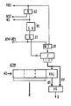
- FIG. 1 The only figure in the drawing shows a schematic representation of an entry line of an address translation memory ATM which can be controlled with the address AD and has the section VAL for the validation character K1, which is fed to the comparator VG each time the entry is activated.
- the instantaneous meter reading supplied by the cyclically operating meter Z serves as the comparison indicator KV. If the two characters match, the data contained in the entered entry but not specified are valid, which is reported in a known manner with the output signal g of the comparator VG to the device (not shown) which further processes the data contained in the entry.
- the associated validity indicator is derived from the output of the counter Z and transferred to the associated section VAL.
- the counter Z is only incremented by a step if all entries in the ATM memory are to be declared invalid. This is done by the ATM-RES signal.
- the comparison indicator KV always deviates from the validity indicator stored in the VAL sections of the memory ATM after a counter advance. All entries are therefore invalid at once, without the individual entries being activated one after the other - as before - and without changing the validity indicators.
- the overflow signal ue which is triggered when the last count position is reached before the counter Z is at zero position and which sets a flip-flop KS via the AND gate U1 with the advance signal ATM-RES which then brings about the zero position.
- the end of this change in entry is reported with the signal NSE, which is transmitted via the AND gate U2 in connection with the set flip-flop then triggers another increment pulse for the counter, which is fed to it via the OR gate 01.
- the flip-flop KS is reset and the memory is released again for normal work.
Landscapes
- Engineering & Computer Science (AREA)
- Theoretical Computer Science (AREA)
- Physics & Mathematics (AREA)
- General Engineering & Computer Science (AREA)
- General Physics & Mathematics (AREA)
- Data Exchanges In Wide-Area Networks (AREA)
- Techniques For Improving Reliability Of Storages (AREA)
Priority Applications (1)
| Application Number | Priority Date | Filing Date | Title |
|---|---|---|---|
| AT84103726T ATE29082T1 (de) | 1983-04-06 | 1984-04-04 | Schaltungsanordnung fuer speichereinrichtungen zur speicherung von daten mit gueltigkeitszeichen. |
Applications Claiming Priority (2)
| Application Number | Priority Date | Filing Date | Title |
|---|---|---|---|
| DE3312391 | 1983-04-06 | ||
| DE3312391A DE3312391C2 (de) | 1983-04-06 | 1983-04-06 | Schaltungsanordnung für Speichereinrichtungen zur Speicherung von Daten mit Gültigkeitskennzeichen |
Publications (2)
| Publication Number | Publication Date |
|---|---|
| EP0123955A1 true EP0123955A1 (fr) | 1984-11-07 |
| EP0123955B1 EP0123955B1 (fr) | 1987-08-19 |
Family
ID=6195603
Family Applications (1)
| Application Number | Title | Priority Date | Filing Date |
|---|---|---|---|
| EP84103726A Expired EP0123955B1 (fr) | 1983-04-06 | 1984-04-04 | Circuit pour dispositifs de mémoire pour la mémorisation de donnée avec un indice de validité |
Country Status (3)
| Country | Link |
|---|---|
| EP (1) | EP0123955B1 (fr) |
| AT (1) | ATE29082T1 (fr) |
| DE (1) | DE3312391C2 (fr) |
Cited By (2)
| Publication number | Priority date | Publication date | Assignee | Title |
|---|---|---|---|---|
| EP0336821A3 (fr) * | 1988-04-04 | 1991-09-04 | EVANS & SUTHERLAND COMPUTER CORPORATION | Système d'antémémoire à utilisation pour ordinateur |
| EP1426867A3 (fr) * | 2002-12-04 | 2006-09-20 | Bull HN Information Systems Inc. | Invalidation rapide de TLB pour adressage de mémoire virtuelle |
-
1983
- 1983-04-06 DE DE3312391A patent/DE3312391C2/de not_active Expired
-
1984
- 1984-04-04 AT AT84103726T patent/ATE29082T1/de not_active IP Right Cessation
- 1984-04-04 EP EP84103726A patent/EP0123955B1/fr not_active Expired
Non-Patent Citations (3)
| Title |
|---|
| IBM TECHNICAL DISCLOSURE BULLETIN, Band 13, Nr. 11, April 1971, Seiten 3380-3381, New York, USA; J.R. DAILEY et al.: "Associative information manipulator" * |
| IBM TECHNICAL DISLOSURE BULLETIN, Band 14, Nr. 2, Juli 1971, Seiten 358-361, New York, USA; J.G. EARLE et al.: "Multiprocessing checkpoint retry" * |
| INFORMATION PROCESSING 68, Proceedings of the I.F.I.P. Congres 68 organised by the International Federation for Information Processing, Edingburgh, 5.-10. August 1968, Seiten 796-800, North-Holland Publishing Company, 1969, Amsterdam, NL; * |
Cited By (2)
| Publication number | Priority date | Publication date | Assignee | Title |
|---|---|---|---|---|
| EP0336821A3 (fr) * | 1988-04-04 | 1991-09-04 | EVANS & SUTHERLAND COMPUTER CORPORATION | Système d'antémémoire à utilisation pour ordinateur |
| EP1426867A3 (fr) * | 2002-12-04 | 2006-09-20 | Bull HN Information Systems Inc. | Invalidation rapide de TLB pour adressage de mémoire virtuelle |
Also Published As
| Publication number | Publication date |
|---|---|
| ATE29082T1 (de) | 1987-09-15 |
| DE3312391A1 (de) | 1984-10-11 |
| EP0123955B1 (fr) | 1987-08-19 |
| DE3312391C2 (de) | 1987-04-02 |
Similar Documents
| Publication | Publication Date | Title |
|---|---|---|
| DE2523414A1 (de) | Hierarchische speicheranordnung | |
| DE2656123C3 (de) | Eingabeeinrichtung zum Zufuhren einer Vielzahl von Zeichen, die ein Datenfeld bilden | |
| DE2418653C3 (de) | Vorrichtung zum Anzeigen eines Extremwertes einer Folge von Digitalwerten | |
| DE2302074A1 (de) | Speicherschutzanordnung in einem multiprozessorsystem | |
| DE2551239C3 (de) | Datenverarbeitungsanlage | |
| DE2756352B2 (de) | Schaltungsanordnung zum Aussuchen und Sortieren von Daten m gleichartig aufgebauten Sätzen | |
| DE2939411C2 (de) | Datenverarbeitungsanlage mit virtueller Speicheradressierung | |
| DE1499182B2 (de) | Datenspeichersystem | |
| DE1474062B2 (de) | Datenverarbeitungsanlage mit einer anzahl von pufferspeichern | |
| DE2703559C2 (fr) | ||
| DE2432608A1 (de) | Speicheranordnung fuer datenverarbeitungseinrichtungen | |
| DE4421640C1 (de) | Hash-Adressierungs- und Speicherverfahren zum Ablegen und Wiedergewinnen von Daten in einem adressierbaren Speicher | |
| DE2729617B2 (de) | Einrichtung zur fortlaufenden Ermittlung eines über eine Meßperiode konstanter Dauer gemittelten Wertes eines Verbrauchs | |
| DE3410496C2 (fr) | ||
| EP0123955B1 (fr) | Circuit pour dispositifs de mémoire pour la mémorisation de donnée avec un indice de validité | |
| EP0026460B1 (fr) | Dispositif de circuit pour adresser des données pour accès de lecture et d'enregistrement dans un système de traitement de données | |
| DE1499170C3 (de) | Datenverarbeitungsanlage | |
| DE2853147C2 (de) | Datenein- und -ausgabeanordnung | |
| DE2639806B1 (de) | Verfahren und einrichtung zum verschluesseln oder entschluesseln von datenbloecken in binaerer darstellung | |
| DE1524179A1 (de) | Einrichtung zur wahlfreien Zusammenstellung und Verteilung von Datenbytes | |
| EP0133569A2 (fr) | Montage pour installations de télécommunications, en particulier centraux téléphoniques avec protection des données par éléments binaires de parité | |
| DE3909267C2 (de) | Schaltungsanordnung für Speichereinrichtungen zur Speicherung von Daten mit Gültigkeitskennzeichen | |
| EP0531559B1 (fr) | Dispositif de commande pour commander une transmission de données entre un, parmi plusieurs modules d'entrée et de sortie et une mémoire de travail d'un dispositif de traitement de données | |
| EP0489248B1 (fr) | Commande d'adresse pour une mémoire à première entrée/première sortie | |
| DE69620834T2 (de) | Abrufvorrichtung zum Holen von Daten aus einem Hauptspeicher |
Legal Events
| Date | Code | Title | Description |
|---|---|---|---|
| PUAI | Public reference made under article 153(3) epc to a published international application that has entered the european phase |
Free format text: ORIGINAL CODE: 0009012 |
|
| AK | Designated contracting states |
Designated state(s): AT BE CH FR GB IT LI NL SE |
|
| 17P | Request for examination filed |
Effective date: 19841128 |
|
| GRAA | (expected) grant |
Free format text: ORIGINAL CODE: 0009210 |
|
| AK | Designated contracting states |
Kind code of ref document: B1 Designated state(s): AT BE CH FR GB IT LI NL SE |
|
| REF | Corresponds to: |
Ref document number: 29082 Country of ref document: AT Date of ref document: 19870915 Kind code of ref document: T |
|
| ET | Fr: translation filed | ||
| ITF | It: translation for a ep patent filed | ||
| PLBE | No opposition filed within time limit |
Free format text: ORIGINAL CODE: 0009261 |
|
| STAA | Information on the status of an ep patent application or granted ep patent |
Free format text: STATUS: NO OPPOSITION FILED WITHIN TIME LIMIT |
|
| 26N | No opposition filed | ||
| ITTA | It: last paid annual fee | ||
| PGFP | Annual fee paid to national office [announced via postgrant information from national office to epo] |
Ref country code: AT Payment date: 19930319 Year of fee payment: 10 |
|
| PGFP | Annual fee paid to national office [announced via postgrant information from national office to epo] |
Ref country code: SE Payment date: 19930422 Year of fee payment: 10 |
|
| PGFP | Annual fee paid to national office [announced via postgrant information from national office to epo] |
Ref country code: FR Payment date: 19930423 Year of fee payment: 10 |
|
| PGFP | Annual fee paid to national office [announced via postgrant information from national office to epo] |
Ref country code: NL Payment date: 19930430 Year of fee payment: 10 |
|
| PGFP | Annual fee paid to national office [announced via postgrant information from national office to epo] |
Ref country code: CH Payment date: 19930712 Year of fee payment: 10 |
|
| PG25 | Lapsed in a contracting state [announced via postgrant information from national office to epo] |
Ref country code: AT Effective date: 19940404 |
|
| PG25 | Lapsed in a contracting state [announced via postgrant information from national office to epo] |
Ref country code: SE Effective date: 19940405 |
|
| PG25 | Lapsed in a contracting state [announced via postgrant information from national office to epo] |
Ref country code: LI Effective date: 19940430 Ref country code: CH Effective date: 19940430 |
|
| PG25 | Lapsed in a contracting state [announced via postgrant information from national office to epo] |
Ref country code: NL Effective date: 19941101 |
|
| NLV4 | Nl: lapsed or anulled due to non-payment of the annual fee | ||
| PG25 | Lapsed in a contracting state [announced via postgrant information from national office to epo] |
Ref country code: FR Effective date: 19941229 |
|
| REG | Reference to a national code |
Ref country code: CH Ref legal event code: PL |
|
| EUG | Se: european patent has lapsed |
Ref document number: 84103726.0 Effective date: 19941110 |
|
| REG | Reference to a national code |
Ref country code: FR Ref legal event code: ST |
|
| PGFP | Annual fee paid to national office [announced via postgrant information from national office to epo] |
Ref country code: GB Payment date: 19950320 Year of fee payment: 12 |
|
| PGFP | Annual fee paid to national office [announced via postgrant information from national office to epo] |
Ref country code: BE Payment date: 19950419 Year of fee payment: 12 |
|
| PG25 | Lapsed in a contracting state [announced via postgrant information from national office to epo] |
Ref country code: GB Effective date: 19960404 |
|
| PG25 | Lapsed in a contracting state [announced via postgrant information from national office to epo] |
Ref country code: BE Effective date: 19960430 |
|
| BERE | Be: lapsed |
Owner name: SIEMENS A.G. BERLIN UND MUNCHEN Effective date: 19960430 |
|
| GBPC | Gb: european patent ceased through non-payment of renewal fee |
Effective date: 19960404 |