EP0124209A1 - Elektronische Ballast-Wechselrichterschaltung - Google Patents
Elektronische Ballast-Wechselrichterschaltung Download PDFInfo
- Publication number
- EP0124209A1 EP0124209A1 EP84301059A EP84301059A EP0124209A1 EP 0124209 A1 EP0124209 A1 EP 0124209A1 EP 84301059 A EP84301059 A EP 84301059A EP 84301059 A EP84301059 A EP 84301059A EP 0124209 A1 EP0124209 A1 EP 0124209A1
- Authority
- EP
- European Patent Office
- Prior art keywords
- transistor
- circuit
- tank circuit
- voltage
- current
- Prior art date
- Legal status (The legal status is an assumption and is not a legal conclusion. Google has not performed a legal analysis and makes no representation as to the accuracy of the status listed.)
- Ceased
Links
Images

Classifications
-
- H—ELECTRICITY
- H05—ELECTRIC TECHNIQUES NOT OTHERWISE PROVIDED FOR
- H05B—ELECTRIC HEATING; ELECTRIC LIGHT SOURCES NOT OTHERWISE PROVIDED FOR; CIRCUIT ARRANGEMENTS FOR ELECTRIC LIGHT SOURCES, IN GENERAL
- H05B41/00—Circuit arrangements or apparatus for igniting or operating discharge lamps
- H05B41/14—Circuit arrangements
- H05B41/26—Circuit arrangements in which the lamp is fed by power derived from DC by means of a converter, e.g. by high-voltage DC
- H05B41/28—Circuit arrangements in which the lamp is fed by power derived from DC by means of a converter, e.g. by high-voltage DC using static converters
- H05B41/282—Circuit arrangements in which the lamp is fed by power derived from DC by means of a converter, e.g. by high-voltage DC using static converters with semiconductor devices
- H05B41/285—Arrangements for protecting lamps or circuits against abnormal operating conditions
- H05B41/2851—Arrangements for protecting lamps or circuits against abnormal operating conditions for protecting the circuit against abnormal operating conditions
- H05B41/2853—Arrangements for protecting lamps or circuits against abnormal operating conditions for protecting the circuit against abnormal operating conditions against abnormal power supply conditions
-
- H—ELECTRICITY
- H02—GENERATION; CONVERSION OR DISTRIBUTION OF ELECTRIC POWER
- H02M—APPARATUS FOR CONVERSION BETWEEN AC AND AC, BETWEEN AC AND DC, OR BETWEEN DC AND DC, AND FOR USE WITH MAINS OR SIMILAR POWER SUPPLY SYSTEMS; CONVERSION OF DC OR AC INPUT POWER INTO SURGE OUTPUT POWER; CONTROL OR REGULATION THEREOF
- H02M7/00—Conversion of AC power input into DC power output; Conversion of DC power input into AC power output
- H02M7/42—Conversion of DC power input into AC power output without possibility of reversal
- H02M7/44—Conversion of DC power input into AC power output without possibility of reversal by static converters
- H02M7/48—Conversion of DC power input into AC power output without possibility of reversal by static converters using discharge tubes with control electrode or semiconductor devices with control electrode
- H02M7/53—Conversion of DC power input into AC power output without possibility of reversal by static converters using discharge tubes with control electrode or semiconductor devices with control electrode using devices of a triode or transistor type requiring continuous application of a control signal
- H02M7/537—Conversion of DC power input into AC power output without possibility of reversal by static converters using discharge tubes with control electrode or semiconductor devices with control electrode using devices of a triode or transistor type requiring continuous application of a control signal using semiconductor devices only, e.g. single switched pulse inverters
- H02M7/5383—Conversion of DC power input into AC power output without possibility of reversal by static converters using discharge tubes with control electrode or semiconductor devices with control electrode using devices of a triode or transistor type requiring continuous application of a control signal using semiconductor devices only, e.g. single switched pulse inverters in a self-oscillating arrangement
- H02M7/53832—Conversion of DC power input into AC power output without possibility of reversal by static converters using discharge tubes with control electrode or semiconductor devices with control electrode using devices of a triode or transistor type requiring continuous application of a control signal using semiconductor devices only, e.g. single switched pulse inverters in a self-oscillating arrangement in a push-pull arrangement
- H02M7/53835—Conversion of DC power input into AC power output without possibility of reversal by static converters using discharge tubes with control electrode or semiconductor devices with control electrode using devices of a triode or transistor type requiring continuous application of a control signal using semiconductor devices only, e.g. single switched pulse inverters in a self-oscillating arrangement in a push-pull arrangement of the parallel type
-
- Y—GENERAL TAGGING OF NEW TECHNOLOGICAL DEVELOPMENTS; GENERAL TAGGING OF CROSS-SECTIONAL TECHNOLOGIES SPANNING OVER SEVERAL SECTIONS OF THE IPC; TECHNICAL SUBJECTS COVERED BY FORMER USPC CROSS-REFERENCE ART COLLECTIONS [XRACs] AND DIGESTS
- Y10—TECHNICAL SUBJECTS COVERED BY FORMER USPC
- Y10S—TECHNICAL SUBJECTS COVERED BY FORMER USPC CROSS-REFERENCE ART COLLECTIONS [XRACs] AND DIGESTS
- Y10S315/00—Electric lamp and discharge devices: systems
- Y10S315/07—Starting and control circuits for gas discharge lamp using transistors
Definitions
- the present invention relates to an electronic ballast-inverter circuit usable for powering fluorescent lamps or the like, and more particularly to an electronic ballast-inverter circuit designed to reduce the high voltage stress on power switching transistors used in the circuit.
- High frequency electronic ballast circuits for powering fluorescent lamps generally provide the advantages of higher efficiencies and smaller size when compared with older 60 Hz ballast circuits.
- These high frequency ballast circuits which usually include DC to AC inverters, have shortcomings in other areas, however, such as in the area of switching losses in the power switching transistors usually used in such applications, when operating at the power levels required by the fluorescent lamps.
- Such circuits have also generally been sensitive to the amplitude of the D C source voltage, in that a change in voltage will adversely affect the frequency of operation of such circuits.
- these circuits generally have a very poor crest factor since they draw current from the AC supply in short bursts every half cycle of the input voltage, whereby the circuit (particularly if a large number of them are used) can adversely affect the input supply waveform. Fourth, it can be difficult to satisfactorily design these circuits to have a sufficiently high power factor. Fifth, where the inverter includes a pair of push-pull transistors, the base drive to each is usually through a resistor, an arrangement which creates an excessive amount of heat under certain conditions.
- bridge inverter instead of the typical parallel transistor inverter.
- the bridge inverter provides the benetit that each transistor in the bridge inverter is subjected only to the voltage supply during cutoff because there is no induced voltage present derived from the operation of the power transformer.
- bridge inverters operate safely with twice the supply voltage for a given transistor type.
- a primary disadvantage of the bridge inverter is its greater complexity, including the fact that it requires four transistors, instead of the two required in a normal parallel inverter, to provide the same power conversion.
- Half bridge converters are known in the art, but they have the disadvantage of being only able to generate a square wave output. Such an output creates harmonic distortion and inefficient power transfer to the fluorescent lamps.
- Half-bridge convertors also do not provide for rapid turn off of the switching transistors, thereby adding to the inefficiencies inherent in such circuits.
- the present invention is directed towards providing the benefits of a bridge inverter in allowing a given transistor type to operate at the equivalent of twice its normal voltage rating, while minimizing the complexity of the circuit, whilst also enabling such operation using only two transistors rather than the four required for a bridge type inverter.
- an inverter circuit for powering one or more fluorescent lamps or the like comprising a DC voltage source including a power input terminal and a ground return terminal; a transformer having first and second primary windings and at least one secondary winding adapted to be connected in series with a fluorescent lamp; a first circuit including a first tank circuit having a predetermined resonant frequency, a first inductor connected in series between one side of said first tank circuit and said power input terminal and a first transistor connected to the other side of said first tank circuit operative when turned on to switchably connect said second side of said first tank circuit to an intermediate potential terminal, said first tank circuit comprising a first capacitor connected in parallel with said first primary winding; a second circuit including a second tank circuit having a resonant frequency identical to said first tank circuit, a second inductor inductively coupled to said first inductor and connected in series between one side of said tank circuit and said intermediate potential terminal, and a second transistor connected to the other side of said second tank circuit operative when turned on to
- the circuit of the present invention will operate at twice its normal voltage rating without the need for the complexity and increased expense of a bridge type inverter.
- the circuit overcomes the disadvantages of prior art circuits in that the frequency of the inverter is substantially independent of the amplitude of the DC source voltage, and, due to the absence of the need to provide smoothing, no electrolytic capacitor is needed across the input to the inverter, thereby improving circuit reliability and efficiency and reducing its cost.
- the circuit may be powdered from a conventional AC power source which is then rectified to provide the DC source voltage used by the inverter circuit lO. It is envisioned that the circuit will be used in areas where higher input voltage levels are experienced, e.g. AC voltage levels on the order of 277 volts RMS.
- the DC source voltage Vl which is input to the inverter circuit 10 at the power input terminal 12, is preferably generated from a conventional rectifier means comprising a full wave diode bridge 14.
- Diode bridge 14 has coupled to it an AC input voltage which is supplied to a pair of input terminals 16 from the AC power source.
- a conventional EMI filter means 18 may be connected between terminals 16 and rectifier means 14.
- a fuse 20 and a thermal cutout switch 22 may also be added to provide further protection for the components of the ballast-inverter circuit 10.
- series inductor 24 and a capacitor 26 may be connected on the output of the rectifier means 14.
- Inductor 24 is connected in series between the output of rectifier means 14 and input terminal 12 and provides further series filtering to filter out any high voltage transients appearing on either side of that inductor.
- Capacitor 26 is added between rectifier means 14 and a ground return terminal 28 to further smooth out the high frequency voltage transients on this line.
- the present invention is operable using a filtered DC source voltage, as described above, it is desirable to operate the present invention, for efficiency of power consumption, from a pulsed DC, i.e. using the unsmoothed AC full wave rectified voltage output by the rectifier means 14.
- Capacitor 26 operates only as a high frequency filter for preventing any signal generated by the ballast-inverter according to the present invention from feeding back onto the AC input power line. It does not filter the input DC voltage in the manner of an electrolytic capacitor. Consequently, the value of this capacitor 26 need only be high enough to provide a low impedance path to the ground return terminal 28 at the high operating frequency of the inverter circuit 10 according to the present invention.
- the ballast-inverter 10 includes two substantially identical circuits shown at 100 and at 200.
- Each circuit 100, 200 is designed to function in an identical way but in alternating cycles of the output sine wave.
- the two circuits 100 and 200 are connected to the input DC voltage source in a manner so as to enable them to operate at different DC offsets from one another.
- the upper circuit 100 is designed to operate off of the voltage amplitude appearing between the power input terminal 12 and an intermediate terminal 30, while the lower circuit 200 is designed to operate off of the voltage amplitude existing between the intermediate terminal 30 and the ground return terminal 28.
- This DC voltage offset is enabled by capacitors 32 and 34, capacitor 32 being connected between the power input terminal 12 and the intermediate terminal 30 and capacitor 34 being connected between the input terminal 30 and the ground return terminal 28.
- the inverter 10 also includes a transformer Tl which includes two 42 turn primary windings, windings 102 and 202, and two 51 turn secondary windings 36 and 38.
- a transformer Tl which includes two 42 turn primary windings, windings 102 and 202, and two 51 turn secondary windings 36 and 38.
- Two fluorescent lamps, indicated at 40 and 42, are shown connected in an exemplary manner in series with the two secondary windings 36 and 38.
- two ballast inductors 44 and 46 which are operable in a conventional manner to enable operation of the fluorescent lamps 40 and 42.
- conventional filament heater secondary windings 48, 50 and 52 for initial heating of the filaments of the fluorescent lamps 40 and 42 to facilitate rapid, non-destructive starting of these lamps.
- a capacitor 54 may be connected in parallel with lamp 40 to substantially short out this lamp during initial start up of the circuit.
- capacitor 54 enables substantially all of the initial voltage generated on start-up to appear only across fluorescent lamp 42 to facilitate its rapid turn on. This is necessary because both lamps initially appear to be substantially open circuits, and do not reduce to a substantially lower impedance until ignition of the lamp has been established. That is, a higher voltage is required to ignite the lamp than is required to maintain its operating state once ignition has occurred. Capacitor 54 facilitates this process.
- the first circuit 100 includes a tank circuit 101 comprising a capacitor 104 in parallel with primary winding 102.
- the values of primary winding 102 and capacitor 104 are chosen to provide a predetermined resonant frequency equal to the desired frequency of operation of the output sinusoid fed to the fluorescent lamp or lamps to be powered by the inverter circuit 10.
- a resonant frequency of at least 20 kHz is preferable for the operation of this circuit.
- the components of this tank circuit are therefore chosen to produce a resonant frequency in this frequency range.
- the first circuit 100 also includes a transistor switch 106 that is associated with the tank circuit 101.
- tank circuit 101 point 128, is connected to the power input terminal 12 via an inductor 108, and the other side of tank circuit 101, point 140, is connected to the collector of transistor 106.
- the emitter of transistor 106 is connected to the intermediate terminal 30.
- some other type of solid state switch such as an SCR or power FET, could be used in place of transistor 106 in circuit 100, in a manner known to those skilled in the art.
- the second circuit 200 also includes a tank circuit, shown at 201, comprising a capacitor 204 in parallel with primary winding 202.
- the values of primary winding 202 and capacitor 204 are chosen to provide the same resonant frequency as that chosen for tank circuit 101.
- the primary windings 102 and 202 need to be closely coupled together to ensure this operation.
- the second circuit 200 also includes a transistor or other solid state switch 206 that is associated with the tank circuit 201. As can be seen, one side of tank circuit 201, point 228, is connected to the intermediate terminal via an inductor 208, and the other side of tank circuit 201, point 240, is connected to the collector of transistor 206.
- the emitter of transistor 206 is connected to the ground return terminal 28.
- Inductors 108 and 208 are necessary to enable the tank circuits 101 and 201 to operate at voltage ranges exceeding the power input voltage Vl.
- inductors 108 and 208 are wound as bifilar windings on a common core to maximize the coupling between these two components.
- the current that is driven through one of these inductors 108, 208 during one half cycle of the inverter according to the present invention needs to be coupled to the other respective inductor 108, 208 during the second half cycle of the inverter. This cross-coupling construction enables this result. Further details concerning the operation of inductors 108 and 208 are given below.
- the base of transistor 106 (as well as transistor 206) is driven from one of four current sources.
- the main current source to transistor 106 comprises capacitor 110, inductor 112 and diode 114, with this network of components providing current during the normal operation of circuit 100 for driving the base of transistor 106 when it is turned on. Two other current sources are provided, and function to start or restart the switching action of transistor 106.
- Capacitor 116, resistor 118 and diodes 120 and 122 operate as a current source to provide current to the base of transistor 106 whenever the DC voltage source V1 at power input terminal 12 has just begun rising from substantially 0 volts (which it will do 120 times a second since it is a 60 Hz signal).
- Resistor 124 provides another current path to start the operation of transistor 106 when power is first coupled to circuit 100 or thereafter if the circuit stalls at some point other than when Vl is approximately 0 volts.
- Voltage dependent resistor 126 provides a fourth current path to the base of transistor 106 to protect transistor 106 if it inadvertently has turned off and the voltage at point 128 at the top of tanK circuit 101 has risen above a predetermined safe level.
- the identical current paths to those described with respect to circuit 100 operation are provided in circuit 200 for driving the base of transistor 206.
- the main current source to transistor 206 comprises capacitor 210, inductor 212 and diode 214, with this network of components providing current during the normal operation of circuit 200 for driving the base of transistor 206 when it is turned on.
- Two other current sources are provided to provide starting current for transistor 206.
- Capacitor 216, resistor 218 and diodes 220 and 222 operate as a current source to provide current to the base of transistor 206 whenever the voltage source at the intermediate point 30 has just begun rising from substantially 0 volts, which it will also do 120 times a second.
- Resistor 224 provides another current path to start the operation of transistor 206 when power is first initiated to circuit 200 or thereafter if the circuit stalls at some point other than when Vl is approximately 0 volts.
- Voltage dependent resistor 226 provides a fourth current path to the base of transistor 206 to protect transistor 206 if it has inadvertently gone off and the voltage at the top of tank circuit 201, indicated as point 228, rises above a predetermined safe level.
- Diode 60 connected between point 228 and the input terminal 12, functions as a clamp to ensure that the voltage at point 228, the top of tank 201, is never significantly higher in voltage than the voltage at terminal 12. This protects the circuit from unexpected voltage transients that may otherwise cause the second circuit 200 to operate at a higher voltage than the first circuit 100.
- an additional primary winding shown at 130 and preferably having one or two turns, is connected between the base of transistor 106 and the intermediate terminal 30 to provide a steering means for this current.
- a diode 132 Also included in series with coil 130 is a diode 132. As will be described in greater detail hereinbelow, coil 130 and diode 132 function to divert base current from transistor 106 during alternate half cycles of the output sine wave, generated by inverter 10, when transistor 106 is to be held off and transistor 206 is on. This is because capacitor 110 and inductor 112 continue to act as a for delivery of current to the base of transistor 106.
- Coil 130 functions to deliver this current out to intermediate terminal 30 when transistor 106 is off since the voltage across the primary windings 102, 202 also appears across coil 130. The polarity of this coil 130 voltage controls this pulling out of current from the base of transistor 106. Diode 132 merely provides a DC offset generating means to match the base to emitter voltage drop of transistor 106.
- another additional primary winding shown at 230, is connected in series with a diode 232 between the base of transistor 206 and the ground return terminal 28 to control the current coupled to the base of transistor 206 and thus provide of the output sine wave generated by the inverter 10 according to the present invention.
- a diode 134 is connected between the base of transistor 106 and point 128 at the top side of the tank circuit 101.
- This diode provides means for causing the rapid switching off of transistor 106 when a half cycle of the output sine wave has been completed.
- This diode functions to pull current out of the base of transistor 106 to provide very rapid turn off of this transistor and to provide a path for the current flowing in this transistor back to the top of tank circuit 101.
- a diode 234 is connected between the base of transistor 206 and point 228 at the top side of tank circuit 201 to provide the same function in circuit 200.
- the ballast-inverter 10 operates in the following manner. For simplicity of description, the operation of only one of the two circuits 100, 200 will be described. It should be understood that the other circuit will operate in essentially an identical manner, but only in an opposite half cycle of the output sine wave, i.e. 180 0 out of phase. During normal operation, with the circuit already operating, both tank circuits 101 and 201 would be oscillating. Assume for the purpose of explanation that transistor 106 has just turned on. Transistor 106 creates thereby a conductive path between its collector, point 140, and the intermediate terminal 30, the ground point for circuit 100. This causes current to flow through the transistor from the tank circuit out to the intermediate terminal 30.
- the other side of the tank circuit, at point 128, is swinging in a half sine wave starting off from 0 volts going through a positive peak of up to 600 volts, depending on the present voltage of the unsmoothed DC voltage Vl, and then back down to 0 volts at the end of the sine wave half cycle.
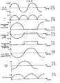
- the frequency of this sine wave corresponds to the resonant frequency of tanK circuit 101. See, e.g., FIGURE 2H, which illustrates an exemplary voltage waveform between point 128 and intermediate terminal 30.
- transisor 106 when transisor 106 goes on, there is no voltage across capacitor 104 since both sides of the capacitor are at 0 volts at that point. That means that at that point there is a maximum current in the primary winding inductor 102. That current flows into capacitor 104 building up its voltage until it reaches a peak, which may be upwards of 600 volts, at the top of the sine wave. The capacitor then begins to discharge, with the current flowing back into inductor 102, causing it to store an increasing amount of current until the voltage again drops to 0. See, e.g., FIGURES 2F and 2G, which illustrate capacitor 104 operation. At that point we would like the transistor 106 to turn off.
- FIGURE 2C illustrates the collector voltage at point 140 of transistor 106.
- FIGURE 2D shows the voltage variation seen at the base of transistor 106.
- inductor 108 acts to couple power to tank circuit 101 and power transistor 106 from the power input terminal during one of two half cycles of the output sine wave (power is coupled to tank circuit 201 and transistor 206 via inductor 208 during the other half cycle).
- transistor 106 When the half cycle when transistor 106 is on, therefore, it causes current to be pulled through inductor 108 and tank circuit 101 essentially independent of the tank circuit current that is normally flowing in the tank.
- An example of the current through transistor 106 is shown in the current curve of FIGURE 2E. It is this latter current that is inductively coupled to secondary windings 36 and 38 of transformer Tl by primary winding 102 to power flourescent lamps 40 and 42.
- Inductor 108 further acts to isolate the sine wave oscillations of tank circuit 101 from the 60 Hz pulsating DC source voltage at the power input terminal 12. Without inductor 108, the voltage across inductor 102 would be limited to the maximum RMS voltage of the DC voltage source. This would cause tank circuit 101 to essentially operate as a square wave inverter rather than a sine wave inverter. In addition, inductor 108 acts to limit the current to tank circuit 101 to thereby protect transistor 106 from drawing a maximum current from the DC power source. Without current limiting, transformer Tl could become saturated, such that the impedance of windings 102 and 202 would disappear. The result would be that the input power source would be connected directly across the collector of transistor 106 without resistive loading, thereby enabling excessive current to flow through transistor 106. The probable result is that transistor 106 would be rapidly destroyed.
- inductor 112 In addition to providing the base current to enable transistor 106 to turn on and stay on during alternate half cycles at the 20kHz tank circuit frequency, inductor 112 also assists in turning on transistor 106 when the DC input voltage Vl at power input terminal 12 goes to 0 volts 120 times a second. After Vl goes to zero volts, inductor 112 continues to output current for a short time. Tank circuit 101 will also generally ring (continue to oscillate) for a short time after power is removed. This ringing helps to steer the current output by inductor 112 and 212 to either transistor 106 or 206, depending on the polarity of the voltage across coils 102 and 202, and thereby the polarity across corresponding coils 130 and 230.
- Capacitor 110 acts as a current source, since point 128 is going from a ground potential up to a high voltage level. Of course, point 128 will make this positive going transition once every cycle at the tank circuit frequency. As previously mentioned, the maximum voltage that point 128 will normally reach depends on the voltage level of the DC input voltage terminal 12, which will vary from a low of 0 volts to a normal high of between 250 and 500 volts. Consequently, for a small capacitor, one normally will obtain a fairly large amount of current passing through capacitor 110, i.e. on the order of 300 milliamps peak, and the current is in the form of a square wave. Diode 114 acts as a half wave rectifier enabling capacitor 110 to conduct current only in the forward direction into inductor 112. In summary, capacitor 110 acts as a source for the primary running current for the base of transistor 106 during its normal switching operation.
- Capacitor 116, resistor 118, and diodes 120 and 122 provide starting current for the base of transistor 106 via inductor 112 at those times when the DC voltage Vl is starting at 0 volts. This current is limited by resistor 118. This current flows through diode 122, inductor 112, and into the base of transistor 106. Diode 122 prevents current generated by capacitor 110 from flowing in any direction except through inductor 112. Diode 120 allows current to flow only in the forward direction through capacitor 116.
- resistor 124 is a high impedance resistor, e.g. 150 kilohms, which is connected in parallel with capacitor 116 and resistor 118. More importantly, however, resistor 124 provides current to the base of transistor 106 if the circuit stalls, i.e. if both transistors 106 and 206 are off at any point other than when the input voltage is at 0 volts. The resistance of resistor 124 is high enough so that little current flows through this resistor during the normal start up operation. This current path is needed because, at higher voltage levels, insufficient current may be available from the starting means, comprising capacitor 116 and resistor 118, to turn on transistor 106 without such assistance.
- the current provided by capacitor 116 is designed to be sufficient to supply enough starting current to drive the base of transistor 106. Since the corresponding components in circuit 200 are designed to supply the same starting current to the . base of transistor 206, and since one of the two transistors 106, 206 will always have a slightly higher gain than the other, the transistor having such higher gain will turn on first. As this transistor goes on, it will cause a voltage drop in the 42 turn winding of its corresponding tank circuit (winding 102 or 202), which then couples this voltage back to steering windings 130 and 230. This reinforces the flow of current into the transistor that has gone on, and ensures that the other transistor remains off for a complete sine wave half cycle.
- resistor 126 Another protective device for transistor 106 is voltage dependent resistor 126.
- Resistor 126 provides another path for current to flow into the base of transistor 106.
- Resistor 126 is designed to operate when current is flowing in inductor 108 and neither transistor 106 and 206 is on. If resistor 126 were not there, this current would cause the voltage at point 128 to rapidly increase to destructive levels. Consequently, resistor 126 operates to create a current path to the base of transistor 106 whenever point 128 goes above a certain predetermined voltage, e.g. 600 volts. At this point, resistor 126 begins to conduct, dumping current into the base of transistor 106. This causes transistor 106 to turn on in the same manner as the starting circuit would.
- a certain predetermined voltage e.g. 600 volts.
- FIGURES 2A-2H illustrate certain of the waveforms present in the electronic ballast circuit 10 according to the present invention.
- FIGURE 2A shows the input 60 Hz AC sine wave power source
- FIGURE 2B illustrates the operation of the rectifier means 14 on this AC input voltage, creating a full wave rectified AC sine wave. This constitutes the unsmoothed 60 Hz DC voltage Vl which appears at power input terminal 12.
- FIGURES 2C-2G illustrate the operation of exemplary portions of circuit 100 according to the present invention. Specifically, FIGURE 2C illustrates the voltage at point 140, the collector of transistor 106, with respect to intermediate terminal 30. This voltage varies at the 20 kHz tank circuit frequency rate, corresponding to the switching rate of transistor 106.
- FIGURE 2D illustrates the voltage appearing at the base of transistor 106. With transistor 106 on, the base is biased slightly positive due to diode 132. When coil 130 changes polarity, the base reflects the increasingly negative voltage across this coil.
- FIGURE 2E illustrates the current flowing through transistor 106 from its collector, point 140, to its emitter, which is tied to intermediate terminal 30, during its normal switching operation.
- FIGURES 2F and 2G illustrate respectively the voltage across, and the current through, capacitor 104 in tank circuit 101. This current is substantially independent of the current that flows through tank circuit 101 and into transistor 106.
- FIGURE 2H illustrates the voltage across the tank circuit and transistor 106, between point 128 and intermediate terminal 30.
Landscapes
- Engineering & Computer Science (AREA)
- Power Engineering (AREA)
- Inverter Devices (AREA)
- Circuit Arrangements For Discharge Lamps (AREA)
Applications Claiming Priority (2)
| Application Number | Priority Date | Filing Date | Title |
|---|---|---|---|
| US472153 | 1983-03-04 | ||
| US06/472,153 US4513226A (en) | 1983-03-04 | 1983-03-04 | Electronic ballast-inverter circuit |
Publications (1)
| Publication Number | Publication Date |
|---|---|
| EP0124209A1 true EP0124209A1 (de) | 1984-11-07 |
Family
ID=23874399
Family Applications (1)
| Application Number | Title | Priority Date | Filing Date |
|---|---|---|---|
| EP84301059A Ceased EP0124209A1 (de) | 1983-03-04 | 1984-02-17 | Elektronische Ballast-Wechselrichterschaltung |
Country Status (3)
| Country | Link |
|---|---|
| US (1) | US4513226A (de) |
| EP (1) | EP0124209A1 (de) |
| JP (1) | JPS59224100A (de) |
Cited By (1)
| Publication number | Priority date | Publication date | Assignee | Title |
|---|---|---|---|---|
| GB2299469A (en) * | 1995-03-06 | 1996-10-02 | Kijima Co Ltd | Output transformer arrangement for a push-pull inverter |
Families Citing this family (18)
| Publication number | Priority date | Publication date | Assignee | Title |
|---|---|---|---|---|
| US5083255A (en) * | 1983-04-22 | 1992-01-21 | Nilssen Ole K | Inverter with electrically controllable output |
| US4663570A (en) * | 1984-08-17 | 1987-05-05 | Lutron Electronics Co., Inc. | High frequency gas discharge lamp dimming ballast |
| JPH01160374A (ja) * | 1987-12-17 | 1989-06-23 | Toshiba Electric Equip Corp | インバータ |
| JP2503588B2 (ja) * | 1988-03-31 | 1996-06-05 | 東芝ライテック株式会社 | 放電灯点灯装置 |
| US5030892A (en) * | 1989-05-03 | 1991-07-09 | Brigham Young University | Means for preventing damage to electronic ballasts as a result of failure of gas discharge lamps |
| US4972124A (en) * | 1990-04-12 | 1990-11-20 | Powers Charles D | Electronic ballast inverter |
| DE59009728D1 (de) * | 1990-07-03 | 1995-11-02 | Siemens Ag | Schaltungsanordnung für ein freischwingendes Sperrwandler-Schaltnetzteil. |
| US5063331A (en) * | 1991-01-04 | 1991-11-05 | North American Philips Corporation | High frequency oscillator-inverter circuit for discharge lamps |
| US5146395A (en) * | 1991-08-09 | 1992-09-08 | Mckie Richard L | Power supply including two tank circuits |
| US6377087B1 (en) * | 1993-01-19 | 2002-04-23 | U.S. Philips Corporation | Driving scheme for bipolar transistors |
| US5557176A (en) * | 1994-01-31 | 1996-09-17 | Diversitec Incorporated | Modulated electronic ballast for driving gas discharge lamps |
| US5461287A (en) * | 1994-02-25 | 1995-10-24 | Energy Savings, Inc. | Booster driven inverter ballast employing the output from the inverter to trigger the booster |
| US5493180A (en) * | 1995-03-31 | 1996-02-20 | Energy Savings, Inc., A Delaware Corporation | Lamp protective, electronic ballast |
| US5877592A (en) * | 1996-11-01 | 1999-03-02 | Magnetek, Inc. | Programmed-start parallel-resonant electronic ballast |
| JPH10285941A (ja) * | 1997-04-04 | 1998-10-23 | Tec Corp | 電源装置 |
| US7286670B2 (en) * | 1999-11-09 | 2007-10-23 | Chaoticom, Inc. | Method and apparatus for chaotic opportunistic lossless compression of data |
| US6359391B1 (en) | 2000-09-08 | 2002-03-19 | Philips Electronics North America Corporation | System and method for overvoltage protection during pulse width modulation dimming of an LCD backlight inverter |
| US6376999B1 (en) | 2000-09-15 | 2002-04-23 | Philips Electronics North America Corporation | Electronic ballast employing a startup transient voltage suppression circuit |
Citations (1)
| Publication number | Priority date | Publication date | Assignee | Title |
|---|---|---|---|---|
| GB898580A (en) * | 1959-08-21 | 1962-06-14 | Gen Electric Co Ltd | Improvements in or relating to circuit arrangements for operating low pressure electric discharge lamps |
Family Cites Families (16)
| Publication number | Priority date | Publication date | Assignee | Title |
|---|---|---|---|---|
| US3754160A (en) * | 1971-10-28 | 1973-08-21 | Radiant Ind Inc | Four-lamp driver circuit for fluorescent lamps |
| US4004187A (en) * | 1974-10-21 | 1977-01-18 | General Electric Company | Push-pull inverter ballast for arc discharge lamps |
| US4060751A (en) * | 1976-03-01 | 1977-11-29 | General Electric Company | Dual mode solid state inverter circuit for starting and ballasting gas discharge lamps |
| US4060752A (en) * | 1976-03-01 | 1977-11-29 | General Electric Company | Discharge lamp auxiliary circuit with dI/dt switching control |
| US4051413A (en) * | 1976-05-26 | 1977-09-27 | Abadie Henry J L | Transistorized static inverters |
| US4127795A (en) * | 1977-08-19 | 1978-11-28 | Gte Sylvania Incorporated | Lamp ballast circuit |
| US4277728A (en) * | 1978-05-08 | 1981-07-07 | Stevens Luminoptics | Power supply for a high intensity discharge or fluorescent lamp |
| US4277726A (en) * | 1978-08-28 | 1981-07-07 | Litton Systems, Inc. | Solid-state ballast for rapid-start type fluorescent lamps |
| US4245177A (en) * | 1978-12-29 | 1981-01-13 | General Electric Company | Inverter for operating a gaseous discharge lamp |
| US4199710A (en) * | 1979-02-12 | 1980-04-22 | Gte Sylvania Incorporated | Ballast circuit for high intensity discharge (HID) lamps |
| US4237403A (en) * | 1979-04-16 | 1980-12-02 | Berkleonics, Inc. | Power supply for fluorescent lamp |
| US4259616A (en) * | 1979-07-09 | 1981-03-31 | Gte Products Corporation | Multiple gaseous lamp electronic ballast circuit |
| US4259614A (en) * | 1979-07-20 | 1981-03-31 | Kohler Thomas P | Electronic ballast-inverter for multiple fluorescent lamps |
| US4469988A (en) * | 1980-06-23 | 1984-09-04 | Cronin Donald L | Electronic ballast having emitter coupled transistors and bias circuit between secondary winding and the emitters |
| JPS5950782A (ja) * | 1982-09-14 | 1984-03-23 | Matsushita Electric Works Ltd | インバ−タ装置 |
| JPS5961483A (ja) * | 1982-09-30 | 1984-04-07 | Ikeda Denki Kk | インバ−タ回路 |
-
1983
- 1983-03-04 US US06/472,153 patent/US4513226A/en not_active Expired - Lifetime
-
1984
- 1984-02-17 EP EP84301059A patent/EP0124209A1/de not_active Ceased
- 1984-02-20 JP JP59030127A patent/JPS59224100A/ja active Pending
Patent Citations (1)
| Publication number | Priority date | Publication date | Assignee | Title |
|---|---|---|---|---|
| GB898580A (en) * | 1959-08-21 | 1962-06-14 | Gen Electric Co Ltd | Improvements in or relating to circuit arrangements for operating low pressure electric discharge lamps |
Non-Patent Citations (2)
| Title |
|---|
| Patent Abstracts of Japan vol. 4, no. 79, 7 June 1980 page 131E14 & JP-A-55-46881 * |
| Patent Abstracts of Japan vol. 7, no. 17, 22 January 1983 & JP-A-57-173383 * |
Cited By (2)
| Publication number | Priority date | Publication date | Assignee | Title |
|---|---|---|---|---|
| GB2299469A (en) * | 1995-03-06 | 1996-10-02 | Kijima Co Ltd | Output transformer arrangement for a push-pull inverter |
| GB2299469B (en) * | 1995-03-06 | 1999-11-03 | Kijima Co Ltd | Push-pull inverter |
Also Published As
| Publication number | Publication date |
|---|---|
| JPS59224100A (ja) | 1984-12-15 |
| US4513226A (en) | 1985-04-23 |
Similar Documents
| Publication | Publication Date | Title |
|---|---|---|
| US4388562A (en) | Electronic ballast circuit | |
| US4513226A (en) | Electronic ballast-inverter circuit | |
| US4857806A (en) | Self-ballasted screw-in fluorescent lamp | |
| US4060751A (en) | Dual mode solid state inverter circuit for starting and ballasting gas discharge lamps | |
| US5313142A (en) | Compact fluorescent lamp with improved power factor | |
| US5747943A (en) | MOS gate driver integrated circuit for ballast circuits | |
| US3753071A (en) | Low cost transistorized inverter | |
| US5148087A (en) | Circuit for driving a gas discharge lamp load | |
| EP0189680A2 (de) | Geregelte Stromversorgung | |
| JPH05508965A (ja) | ガス放電ランプ負荷を駆動する回路 | |
| WO1994010823A1 (en) | A circuit for driving gas discharge lamps having protection against diode operation of the lamps | |
| US4408270A (en) | Stored charge inverter circuit with rapid switching | |
| US6211625B1 (en) | Electronic ballast with over-voltage protection | |
| US5341067A (en) | Electronic ballast with trapezoidal voltage waveform | |
| US4042855A (en) | High frequency transistor ballast | |
| US5019959A (en) | Ballast circuit | |
| US4503361A (en) | Electronic ballast system | |
| US5962985A (en) | DC/AC converter with improved starter circuit | |
| GB2261332A (en) | Driving circuits for discharge devices | |
| US6211619B1 (en) | Electronic ballast cathode heating circuit | |
| US5510680A (en) | Electronic ballast with special voltage waveforms | |
| US5032767A (en) | High frequency oscillator-inverter with improved regenerative power supply | |
| US4961029A (en) | Discharge lamp lighting device | |
| US5343123A (en) | Series-resonant inverter ballast | |
| EP0606665B1 (de) | Schaltung |
Legal Events
| Date | Code | Title | Description |
|---|---|---|---|
| PUAI | Public reference made under article 153(3) epc to a published international application that has entered the european phase |
Free format text: ORIGINAL CODE: 0009012 |
|
| AK | Designated contracting states |
Designated state(s): AT CH DE FR GB IT LI LU NL SE |
|
| 17P | Request for examination filed |
Effective date: 19850507 |
|
| RAP1 | Party data changed (applicant data changed or rights of an application transferred) |
Owner name: ASTEC COMPONENTS LTD. |
|
| STAA | Information on the status of an ep patent application or granted ep patent |
Free format text: STATUS: THE APPLICATION HAS BEEN REFUSED |
|
| 18R | Application refused |
Effective date: 19870514 |
|
| RIN1 | Information on inventor provided before grant (corrected) |
Inventor name: JOSEPHSON, ELLIOT |