EP0124281B1 - Einrichtung und Verfahren zur Aussetzfehlerausgleichung - Google Patents
Einrichtung und Verfahren zur Aussetzfehlerausgleichung Download PDFInfo
- Publication number
- EP0124281B1 EP0124281B1 EP84302201A EP84302201A EP0124281B1 EP 0124281 B1 EP0124281 B1 EP 0124281B1 EP 84302201 A EP84302201 A EP 84302201A EP 84302201 A EP84302201 A EP 84302201A EP 0124281 B1 EP0124281 B1 EP 0124281B1
- Authority
- EP
- European Patent Office
- Prior art keywords
- dropout
- sample
- characteristic
- digital
- digital data
- Prior art date
- Legal status (The legal status is an assumption and is not a legal conclusion. Google has not performed a legal analysis and makes no representation as to the accuracy of the status listed.)
- Expired
Links
- 238000000034 method Methods 0.000 title claims description 15
- 230000004044 response Effects 0.000 claims description 9
- 238000001514 detection method Methods 0.000 claims description 3
- 238000006467 substitution reaction Methods 0.000 claims description 2
- 238000012545 processing Methods 0.000 description 6
- 238000010586 diagram Methods 0.000 description 4
- 239000002131 composite material Substances 0.000 description 3
- 230000000694 effects Effects 0.000 description 3
- 238000012546 transfer Methods 0.000 description 3
- 238000012937 correction Methods 0.000 description 1
- 230000007547 defect Effects 0.000 description 1
- 230000003111 delayed effect Effects 0.000 description 1
- 230000001419 dependent effect Effects 0.000 description 1
- 238000013461 design Methods 0.000 description 1
- 230000006870 function Effects 0.000 description 1
- 238000005070 sampling Methods 0.000 description 1
Images


Classifications
-
- H—ELECTRICITY
- H04—ELECTRIC COMMUNICATION TECHNIQUE
- H04N—PICTORIAL COMMUNICATION, e.g. TELEVISION
- H04N9/00—Details of colour television systems
- H04N9/79—Processing of colour television signals in connection with recording
- H04N9/87—Regeneration of colour television signals
- H04N9/88—Signal drop-out compensation
- H04N9/888—Signal drop-out compensation for signals recorded by pulse code modulation
Definitions
- the invention relates to dropout compensation and particularly to dropout compensation performed at the read side of a time base corrector memory, wherein dropout timing is preserved by selectively encoding the incoming video data.
- dropout compensation In the field of color television, the process commonly known as dropout compensation is performed during the reproduction of video signals.
- the corresponding dropout compensators provide compensation by replacing an incorrect or missing portion of the color television signal, commonly called a "dropout", which is caused by an improper recording or reproduction process, or by a defect in the recording medium.
- a dropout an incorrect or missing portion of the color television signal
- disturbing effects which would be caused in a television picture by the presence of such a dropout, and which are readily seen by a viewer, are removed by the dropout compensation process.
- Typical of such process and apparatus for performing digital dropout compensation is the system described, for example, in U.S. Pat. No. 4,251,831 to B.Y.
- Kamath wherein a suitable band-pass filter, and a dropout compensator employing the filter, provide digital circuits for separating the components of a composite signal for further processing, and for subsequently recombining the components to reconstitute an altered composite signal during reproduction from magnetic tape.
- dropout compensators In order to perform the dropout compensation process, the location of the dropout must be detected and preserved; that is, dropout timing must be preserved to allow subsequently replacing the specific incorrect video data with dropout corrected video data. Since dropout timing inherently is related to tape input video, dropout compensators traditionally have been placed on the input, i.e., write side, of the time base corrector memory employed in a conventional video processing system. Since the input clock of a video signal being read from tape is highly unstable and capable of varying rates of, for example, from 0.5 to 1.7 times normal, as when operating in the high speed shuttle mode, complex counters and very high speed memory are required in a dropout compensator located at the write side of memory in order to perform the dropout compensation process.
- the dropout compensator when the dropout compensator is at the write side of memory it is more dependent upon tape speed. That is, the voltage controlled oscillator located at the input to memory, produces a clock that is continously changing wth tape speed as it tries to track the video information played back from the tape. It follows that the dropout compensator circuit must also operate with the unstable clock, particularly when in the shuttle mode of operation. The dropout compensator circuit must be capable of operating over a wide range of frequencies corresponding to the range of tape speeds and the resulting unstable high rate input clock, and is therefore subject to the requirement for complex counters and the very high speed memory of previous mention.
- the dropout compensator system on the output or read side of memory, since the read clock for the memory always operates at a fixed frequency; for example, at 14.3 megaHertz, for a system in which a color television signal is sampled at four times the color sub-carrier frequency. Since a stable clock of fixed frequency is available at the read side of the memory, a dropout compensator of simplified design, with reduced memory speed requirements, may be utilized. However, since the read and write operations, and thus the timing thereof, are operating independently of each other, preserving the location of the dropout on the write side of memory and transferring thetiming information to the read side of memory, becomes a problem.
- time base correction systems typically read out the stored digital vide several lines later relative to the location in which the data was loaded into memory.
- the initial dropout location that is, the delayed timing information indicative thereof, must be transferred with precision to the output side of memory.
- Time base corrector systems are available wherein the dropout compensator is disposed at the read side of memory.
- the dropout timing information is transferred from the write to the read side of memory by employing a separate dropout memory and memory control to preserve and transfer the dropout timing information, which is loaded into the dropout memory, while video data is being written into the memory of the time-base corrector.
- the dropout timing information is simultaneously extracted from the dropout memory, whereby the time of occurrence of dropouts in the video data is detected, and dropout compensation is effected. It may be seen that in such systems the location of the dropout compensator at the rear side of memory requires an extra memory and associated control circuit in order to preserve the timing information.
- the invention provides a method of compensating for a dropout in video signal, in which the video signal is converted to or is in the form of a succession of digital data samples, is stored and is subsequently readout from storage and a dropout is compensated by substitution of data, characterised in that the dropout is identified by representation within the video signal by at least one digital data sample of predetermined characteristic value.
- the invention provides a system for compensating dropouts in a video signal converted to digital data samples, comprising means for identifying a dropout; memory means for storing an indication of the dropout and for storing the digital data samples; means for detecting the indication of the dropout during read out from the memory means of the stored digital data samples; and means for replacing the dropout sample with a valid digital data sample; characterised in that the means for identifying the dropout provides a digital data sample of characteristic value for representing the dropout and the memory means is arranged to store this characteristic dropout sample within the digital data samples that represent the video signal.
- the present invention generally provides transfer of the dropout information to the read side of memory by modifying video data samples to preserve the time of occurrence of a dropout. It is convenient to transfer the dropout timing information, in an 8-bit system, by assigning an incorrect video data sample the maximum or minimum digital value of 255 or zero, respectively, and inserting the sample in the video data path.
- the occurrence of a dropout may be represented as a digital word, within the video data path, of all "1"s or all "0"s, whereupon the word is subsequently detected by sensing the all "1"s or all "0”s.
- a dropout compensator system may be located at the read side of a time-base corrector memory, the video data is selectively encoded as it is being written into memory to indicate the exact location of a dropout, or dropouts.
- the video samples are modified to provide a digital value which is indicative of the occurrence of the dropout.
- the invention contemplates the use of an 8-bit data sample with the maximum digital value of 255 corresponding to all "1" bits (FFH in the hex notation) to indicate that a dropout has occurred.
- valid video data is precluded from using the value of 255, but is limited to a maximum digital value of 254, i.e., FEH in the hex notation.
- the value 255 (FFH) indicative of the dropout is inserted in the video data path along with the valid video data.
- the value 255 readily is detected on the read side of memory and is used to activate the associated dropout compensator circuit to replace the incorrect video data with dropout compensated video data.
- One advantage of the present invention is that it is now convenient to locate a dropout compensator system at the read side of a memory such as a time-base corrector memory; moreover, it is possible to avoid the use of a separate dropout memory and control therefor, while precisely transferring the dropout timing information to the read side of memory. It is also convenient to operate a dropout compensator with the stable read clock of fixed frequency on the output side of memory.
- the dropout compensator (DOC) of the invention allows the dropout compensator (DOC) of the invention to always read out video data from memory using a stable reference clock.
- the read clock is 14.3 MHz.
- the dropout timing information must be transferred to the read side of memory, since reading out of the video data is conducted several lines after the memory has been loaded.
- the invention provides a relatively simple technique and circuit for effectively realizing the above features.
- the system is described hereinbelow in a typical digital video processing system employing 8-bit data samples, whereby accordingly, the digital sample values normally used to represent the video data range from zero to 255, and a sample rate of 4Fsc (four times sub-carrier frequency) but by way of example only.
- the digital sample values representing the video data are limited to the range of zero to 254, i.e., are limited to FEH in the conventional hex notation. It follows that even if the analog-to-digital (A/D) converter were overloaded with video levels higher than it can sample, the maximum sample value employed to represent the video signal is FEH, i.e., the digital value 254.
- the digital value FFH corresponding to the maximum digital sample value 255, thus is available and is assigned as a characteristic dropout sample to represent the occurrence of a dropout at the particular sample time interval. Since FFH is assigned to represent a dropout, its presence in a video data stream indicates that the corresponding sample, or samples, etc, are invalid video.
- a dropout is detected in conventional fashion; for example, by means of an RF envelope level detector which monitors the amplitude level of the modulated television signal carrier waveform.
- the incorrect video data is replaced with the digital value 255, corresponding to all "1"s in the 8-bit word system employed by way of example only in the description herein.
- the system of the invention may employ the digital value of zero, i.e., a digital sample of all "0"s, to represent the dropout.
- the dropout may be represented by a unique digital value which lies at either end of the range of digital values normally used to represent the video data samples. Since the digital "dropout" sample is inserted in the video data path, its presence at the read side of memory relative to the video data, is precisely at the location at which the dropout occurred on the write side of memory. It is 'therefore a readily simple matter to detect the maximum or minimum digital value at the read side of memory, whereby dropout compensation may be performed to replace the incorrect video with dropout compensated video in generally conventional fashion.
- the invention further contemplates assigning to the dropout sample a digital value which lies within the range of digital values, and which is detected during read out.
- the encoding scheme replaces the valid video sample with 255 or with zero.
- the valid video can be limited to a more resticted range if desired; for example to a range of zero to 253, or 2 to 254, etc.
- the invention contemplates assigning any digital value to the unique dropout sample within the range employed to represent valid video.
- the invention combination provides the further advantage of not having to keep track of the dropout timing information, but to simply monitor the video data as it is read from memory to detect the unique dropout samples.
- a generally conventional time base corrector (TBC) memory system 10 is disposed to receive digitized video data in response to a write clock, and to provide read out of temporarily stored digital video data in response to a read clock.
- TBC time base corrector
- Such memory system as well as address and clocking control therefor, may be found in the aforementioned U.S. Patent No. 4,251,831.
- Digital input video data from off-tape is provided on an 8-bit input data bus 12, which is coupled to a first data path through an input switch means 14.
- An FFH input 16 is coupled to a second data path through the switch means 14, and provides, in effect, the unique dropout sample FFH upon the occurrence of a dropout, as further described in FIGURE 3.
- the input switch means 14 is controlled via a dropout (DO) signal on a control line 18, which is supplied by the video.tape recorder system, and particularly by an RF envelope level detector which monitors the amplitude level of the modulated television signal carrier waveform and herein supplies a logic low in the event of a dropout.
- DO dropout
- switch means 14 inserts the digital value FFH from line 16 into the video data stream in a data bus 17, in place of the incorrect sample or samples of incoming video data on bus 12.
- the valid video data samples, along with the dropout samples, are clocked into the TBC memory system 10 via a write clock on a line 20, which comprises the 4Fsc timing clock conventionally derived off-tape.
- the write clock is generally unstable and capable of rates varying from below normal to 1.7 times normal as when the tape is being pulled at shuttle speeds.
- the video and dropout sample data are supplied via a bus 22 from TBC memory system 10 to a dropout detector means 26, i.e., a value FFH, etc., detector, which detects ne dropout sample corresponding to the presence of a dropout.
- An output switch means 28 is depicted as coupled at a first data path thereof to the dropout detector means 26.
- a video data output corresponding to valid video data, or dropout compensated (DOC) video data is provided on an output data bus 30.
- Dropout compensator means 32 which may be of generally conventional configuration, is coupled to the output data bus 30, and thence back to a second data path through the output switch means 28.
- a control signal is supplied from the detector 26 to the output switch means 28 via a control line 34.
- the TBC memory system 10 is read out in response to a read clock on a line 36, which clock is supplied by a reference timing source 38.
- the latter provides the stable read clock at a fixed frequency such as, in this example, the reference 4Fsc frequency of 14.3 MHz corresponding to the data sample rate of the tape recorder system.
- the reference timing source 38 also provides a timing control (which may be the same 4Fsc read clock) via a line 40 to the dropout compensator means 32, to synchronize the operation thereof with the unloading of the TBC memory system 10.
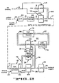
- FIGURE 2 there is shown in greater detail the combination of FIGURE 1, wherein like components are similarly numbered. Accordingly, composite video from off-tape in the analog domain is supplied on an input line 42, extending to an A/D converter 44.
- the components video signal is digitized via the A/D converter 44 at the 4Fsc sample rate used by way of description, and is supplied on input data bus 13 to digital value limiter means 46 as successive 8-bit digital video data samples.
- the limiter means 46 is coupled to a first tri-state input latch 52 corresponding to part of the input switch means 14 of FIGURE 1.
- a second tri-state input latch 54 has coupled thereto the FFH input 16which, in effect, provides the unique dropout value 255 corresponding to the presence of a dropout.
- the tri-state input latches 52, 54 are controlled via the dropout signal of previous mention on the control line 18. Thus, the presence of a low logic state on the line 18 indicates the occurrence of a dropout, whereby tri-state input
- latch 52 is turned off and tri-state input latch 54 is turned on.
- the incorrect video sample or samples on input data bus 12 thus are replaced with a sample or samples of the digitial value 255, via a bus 66 coupled from latch 54 to the video data bus 17.
- the video data bus 17 is coupled to the write side of the TBC memory system 10.
- the write clock on line 20, and the read clock on line 36 provide loading and readout, respectively, of video data samples along with the unique dropout samples FFH which were inserted upon the occurrence of dropouts.
- the data are read from the memory system 10 at the fixed read rate of reference 4Fsc and are fed via a data bus 64 to a first tri-state output latch 68, as well as to the dropout detector means 26 of previous mention.
- the latter has a dropout compensator (DOC) on/ off switch 70 which provides for disabling the dropout detector means 26.
- DOC dropout compensator
- valid video data are supplied from the output of the tristate output latch 68 to an output bus data latch 72, and thence to the output data bus 30.
- the valid video data also are fed to the input of the dropout compensator means 32 of FIGURE 1, via a tri-state data bus 74.
- the data bus 74 is coupled to a DOC memory/ control means 76 and thence to a DOC digital transversal filter means 78 via a DOC memory data bus 77.
- the output of the transversal filter means 78 is supplied via a filter output bus 80 to a second tri-state output latch 82.
- the tri-state output latches 68 and 82 comprise the output switch means 28 of FIGURE 1.
- the tri-state output latch 82 provides dropout corrected video data back to the DOC memory/control means 76 in the event the dropout detector means 26 continues to detect the unique dropout sample.
- the dropout corrected video data is also supplied to the output bus data latch 72 via the tri-state data bus 74.
- the conditions of the tri-state output latches 68, 82 are controlled via the logic state on the control lines 34 extending from the dropout detector means 26.
- the dropout compensator means 32 of FIGURES 1 and 2 are typified by dropout compensators conventionally known in the art and shown, for example, in the U.S. patent 4,251,831 and the AVR-2 catalog of previous mention.
- the dropout compensator means 32 may replace one or more samples in a line of video data, or may replace an entire line, or lines of video data, if such lines have incorrect video throughout.
- the DOC memory/control means 76 may include a one-line delay, wherein the video data is fed to the DOC digital transversal filter means 78 for processing of the chrominance component in conventional fashion to preserve the phase relationship between chrominance and luminance when processing different lines of video data.
- the chrominance and luminance components are then re-combined and supplied via bus 80 and latch 82 to the latch 72. Since the dropout compensator means 32 and the associated process of luminance and chrominance component processing per se are generally conventional and described in the above-mentioned references, which are incorporated herein by reference, no further description is included herein.
- FIGURE 3 includes in greater detail the means for selectively encoding the video data samples, to define a particular dropout sample indicative of the occurrence of a dropout.
- the means include one implementation of the limiter means 46 by way of example only.
- input data bus 13 is coupled to an input bus latch 84 and thence to the tri-state input latch 52 of the input data bus 12.
- the output of latch 52 couples to the data bus 17 of the previous figures.
- the limiter means 46 for encoding the unique dropout sample and for limiting the valid video samples to FEH generally extend from the input data bus 12 to provide control signals to the tri-state input latches 52, 54.
- a NAND gate 88 includes seven inputs corresponding to the seven most significant bit (MSB) lines of the data bus 12, and further includes an eighth or least significant bit (LSB) input coupled to the control line 18 extending from the tape recorder system.
- the output of the NAND gate 88 is coupled to one input of an OR gate 90, whose output is coupled to the inputs of a pair of latches 92, 94.
- the second input of OR gate 90 is coupled to the dropout control line 18.
- the output of NAND gate 88 also is coupled to the LSB input of the tri-state input latch 54.
- the true output of the latch 92 is coupled to the control input of the tri-state input latch 52, while the not-true output of the latch 94 is coupled to the control input of the tri-state input latch 54.
- the seven MSB inputs of the input latch 54 are coupled to a +5 volt source, which supplies thus seven digital "1"s corresponding to the seven MSB of the unique dropout sample FFH.
- the output of the tri-state input latch 54 is coupled via the bus 66 to the data bus 17.
- the input bus latch 84, latches 92,94 and the tri-state input latches 52, 54 all are clocked by the off-tape 4Fsc timing clock on a clock line 95.
- the dropout signal on the control line 18 is a logical high, which places a digital "1" on the LSB input of the NAND gate 88, as well as on the second input to the OR gate 90.
- the NAND gate 88 detects eight "1"s at its input, which is indicative at NAND gate 88, that the video data should be limited since no dropout exists.
- the limiter means 46 must limit the valid video samples to a digital value of 254 (FEH).
- the NAND gate 88 supplies a low to one input of the OR gate 90, therefore providing a high logic level at its output.
- high logic levels are applied to the inputs of the latches 92, 94 which in turn, turn off the tri-state input latch 52 and turn on the tri-state input latch 54, respectively.
- the tri-state input latch 54 how-
- the output of the tri-state input latch 54 comprises seven “1”s and a "0" at its LSB, thereby supplying the digital sample value of 254 corresponding to FEH to the data bus 17. This is indicative of valid video data, and thus a dropout is not indicated.
- the dropout signal on control line 18 goes low, which places a zero on the LSB input of the NAND gate 88.
- the latter places a high on the first input of the OR gate 90, which however, also receives a low from the control line 18 on its second input.
- the OR gate 90 thus supplies a high to the latches 92, 94 which supply a high to the tri-state input latch 52 to turn it off, and a low to the tri-state input latch 54 to turn it on. Since a dropout is detected, the tri-state input latch 54 now receives a "1" at its LSB input as supplied by the high on the output of NAND gate 88.
- the tri-state input latch 54 now supplies an output of eight "1"s, i.e., FFH, to the data bus 17, which is indicative of a dropout and the fact that incorrect video data is on the data bus 12.
- the incorrect data sample is replaced by the unique dropout sample FFH which is inserted into the data stream on the data bus 17 and is supplied to the TBC memory system 10 for storage along with the valid video data samples, as previously described in FIGURE 2.
- FIGURE 4 there is included a schematic of the dropout detector means 26 and the tri-state output latches 68, 82 of FIGURE 2.
- the circuit provides means for detecting the unique dropout sample inserted in the valid video data supplied via the data bus 17 and read out from the TBC memory system 10 via the data bus 64. More particularly, the data bus 64 supplies the 8-bit samples from the memory to a detector NAND gate 96 which, in turn, is coupled to a latch 98 which provides suitable delay to allow switching of the tri-state output latches 68, 82 on the next incoming clock pulse after detection of the dropout.
- the true output of latch 98 is coupled to the control input of tri-state output latch 82, while the not-true output thereof is coupled to the tri-state output latch 68.
- the DOC on/off switch 70 is coupled to the latch 98 to disable the latter.
- a zero is supplied to the LSB input of the NAND gate 96.
- the latter supplies a high to the latch 98 which allows the tri-state output latch 68 to pass valid video data to the output bus data latch 72 and the output data bus 30.
- a unique dropout sample i.e., FFH
- the latch 98 turns off the tri-state output latch 68 and turns on the tri-state output latch 82.
- dropout corrected video data from the dropout compensator means 32 is supplied via the tri-state output latch 82 and the data bus 74 to replace the corresponding dropout sample.
- tri-state latches are shown herein for latches 52, 54, 68 and 82, same may be replaced by multiplexing circuits configured to receive respective input buses and to switch therebetween to provide the functions of the latches in response to control signals from the respective controlling devices, viz, limiter means 46 and dropout detector means 26.
- system of the invention may be used in other than 8-bit digital systems.
- the unique dropout sample would be assigned the value FH in hex notation; a 12-bit system would use the value FFFH, etc.
Landscapes
- Engineering & Computer Science (AREA)
- Multimedia (AREA)
- Signal Processing (AREA)
- Television Signal Processing For Recording (AREA)
- Preparation Of Compounds By Using Micro-Organisms (AREA)
- Radio Transmission System (AREA)
Claims (15)
Applications Claiming Priority (2)
| Application Number | Priority Date | Filing Date | Title |
|---|---|---|---|
| US483060 | 1983-04-06 | ||
| US06/483,060 US4591925A (en) | 1983-04-06 | 1983-04-06 | Encoded dropout compensator system |
Publications (3)
| Publication Number | Publication Date |
|---|---|
| EP0124281A2 EP0124281A2 (de) | 1984-11-07 |
| EP0124281A3 EP0124281A3 (en) | 1986-03-05 |
| EP0124281B1 true EP0124281B1 (de) | 1989-11-02 |
Family
ID=23918480
Family Applications (1)
| Application Number | Title | Priority Date | Filing Date |
|---|---|---|---|
| EP84302201A Expired EP0124281B1 (de) | 1983-04-06 | 1984-03-30 | Einrichtung und Verfahren zur Aussetzfehlerausgleichung |
Country Status (4)
| Country | Link |
|---|---|
| US (1) | US4591925A (de) |
| EP (1) | EP0124281B1 (de) |
| JP (1) | JPS59198512A (de) |
| DE (1) | DE3480373D1 (de) |
Cited By (1)
| Publication number | Priority date | Publication date | Assignee | Title |
|---|---|---|---|---|
| DE19736517A1 (de) * | 1997-08-22 | 1999-02-25 | Alsthom Cge Alcatel | Verfahren zur Reduzierung von Störungen bei der Übertragung eines elektrischen Nachrichtensignals |
Families Citing this family (12)
| Publication number | Priority date | Publication date | Assignee | Title |
|---|---|---|---|---|
| JPS6169286A (ja) * | 1984-09-13 | 1986-04-09 | Sony Corp | ドロツプアウト補正装置 |
| US4864422A (en) * | 1985-09-21 | 1989-09-05 | Robert Bosch Gmbh | Processor for video signals obtained from an information carrier such as a magnetic tape |
| JP2537181B2 (ja) * | 1985-10-08 | 1996-09-25 | キヤノン株式会社 | 映像信号補正装置 |
| US4716454A (en) * | 1985-10-17 | 1987-12-29 | Ampex Corporation | Chroma phase word encode/decode in a video processing system |
| EP0283282B1 (de) * | 1987-03-20 | 1993-05-26 | Pioneer Electronic Corporation | Ausfall-Detektorschaltung |
| NL8801206A (nl) * | 1988-05-09 | 1989-12-01 | Philips Nv | Drop-out kompensatieschakeling. |
| US5239422A (en) * | 1989-04-28 | 1993-08-24 | Pioneer Electronic Corporation | Rotary head type digital magnetic recording-reproducing apparatus |
| SG45361A1 (en) * | 1989-05-16 | 1998-01-16 | Canon Kk | Device for processing transmitted digital video signal |
| JPH0391170A (ja) * | 1989-09-01 | 1991-04-16 | Hitachi Ltd | Pcm信号再生装置 |
| JPH0767181B2 (ja) * | 1989-09-19 | 1995-07-19 | 株式会社東芝 | 再生fm信号処理用半導体集積回路 |
| JP2688725B2 (ja) * | 1991-05-07 | 1997-12-10 | シャープ株式会社 | 映像信号記録再生装置 |
| US5451999A (en) * | 1992-11-05 | 1995-09-19 | Ampex Corporation | Method and apparatus for detecting stability of a digital component video signal |
Family Cites Families (7)
| Publication number | Priority date | Publication date | Assignee | Title |
|---|---|---|---|---|
| US4054903A (en) * | 1975-07-11 | 1977-10-18 | Sony Corporation | Video time base corrector |
| GB2008888B (en) * | 1977-10-27 | 1982-06-30 | Quantel Ltd | Drop-out compensation system |
| JPS54143017A (en) * | 1978-04-28 | 1979-11-07 | Sony Corp | Time base error correction unit |
| US4251831A (en) * | 1979-10-26 | 1981-02-17 | Kamath Bantval Y | Filter and system incorporating the filter for processing discrete samples of composite signals |
| JPS5683154A (en) * | 1979-12-07 | 1981-07-07 | Sony Corp | Transmission method for pcm data |
| JPS5750307A (en) * | 1980-09-05 | 1982-03-24 | Sony Corp | Time base correcting device |
| US4477842A (en) * | 1981-04-20 | 1984-10-16 | Victor Company Of Japan, Ltd. | Data reproducing circuit |
-
1983
- 1983-04-06 US US06/483,060 patent/US4591925A/en not_active Expired - Lifetime
-
1984
- 1984-03-30 EP EP84302201A patent/EP0124281B1/de not_active Expired
- 1984-03-30 DE DE8484302201T patent/DE3480373D1/de not_active Expired
- 1984-04-05 JP JP59068344A patent/JPS59198512A/ja active Pending
Cited By (1)
| Publication number | Priority date | Publication date | Assignee | Title |
|---|---|---|---|---|
| DE19736517A1 (de) * | 1997-08-22 | 1999-02-25 | Alsthom Cge Alcatel | Verfahren zur Reduzierung von Störungen bei der Übertragung eines elektrischen Nachrichtensignals |
Also Published As
| Publication number | Publication date |
|---|---|
| JPS59198512A (ja) | 1984-11-10 |
| US4591925A (en) | 1986-05-27 |
| EP0124281A3 (en) | 1986-03-05 |
| DE3480373D1 (en) | 1989-12-07 |
| EP0124281A2 (de) | 1984-11-07 |
Similar Documents
| Publication | Publication Date | Title |
|---|---|---|
| US4414677A (en) | Synchronization word extractor | |
| US4199780A (en) | Video drop out compensator incorporating digital field storage | |
| US4591925A (en) | Encoded dropout compensator system | |
| USRE34810E (en) | Fast acting phase shifting apparatus for use in digital sampling systems | |
| US4212027A (en) | Time base compensator | |
| US4203076A (en) | Clock pulse signal generator having an automatic frequency control circuit | |
| EP0065365A2 (de) | Digitaler Fernsehapparat | |
| US4053926A (en) | Timing error compensator | |
| CA1086422A (en) | Video time base corrector | |
| US4698698A (en) | Digital television signal processing apparatus | |
| EP0044713B1 (de) | Schaltungsanordnungen zur Verarbeitung digitaler Daten | |
| US5142377A (en) | Time base correction apparatus | |
| JPS6258196B2 (de) | ||
| US4315331A (en) | Apparatus for providing drop-out compensation in recording and reproducing systems | |
| US5121207A (en) | Digital circuit arrangement for processing an analog video signal at a free running system clock | |
| US5034823A (en) | Drop-out compensation circuit | |
| US4849833A (en) | Image signal recording apparatus | |
| JPS5883489A (ja) | Palフオ−マツトビデオ情報信号におけるサンプリングおよびドロツプアウト補償並びに誤り隠閉を行なう装置 | |
| US5587804A (en) | Reproduction error correction circuit for a video reproduction system & the method for operating it | |
| EP0432668B1 (de) | Vorrichtung und Verfahren zur Videosignalverarbeitung für Zeitbasiskompensation | |
| US5497200A (en) | Digital time base corrector | |
| KR0169618B1 (ko) | 스큐 보상 및 잡음을 제거하기 위한 영상신호 처리장치 | |
| US4321704A (en) | Parity checking circuitry for use in multi-bit cell PCM recording and reproducing apparatus | |
| JPS60105386A (ja) | 情報信号の時間軸を変更する装置 | |
| US5606426A (en) | Digital time base corrector for reproducing video signals |
Legal Events
| Date | Code | Title | Description |
|---|---|---|---|
| PUAI | Public reference made under article 153(3) epc to a published international application that has entered the european phase |
Free format text: ORIGINAL CODE: 0009012 |
|
| AK | Designated contracting states |
Designated state(s): CH DE FR GB LI NL |
|
| PUAL | Search report despatched |
Free format text: ORIGINAL CODE: 0009013 |
|
| AK | Designated contracting states |
Kind code of ref document: A3 Designated state(s): CH DE FR GB LI NL |
|
| 17P | Request for examination filed |
Effective date: 19860807 |
|
| 17Q | First examination report despatched |
Effective date: 19880324 |
|
| GRAA | (expected) grant |
Free format text: ORIGINAL CODE: 0009210 |
|
| AK | Designated contracting states |
Kind code of ref document: B1 Designated state(s): CH DE FR GB LI NL |
|
| REF | Corresponds to: |
Ref document number: 3480373 Country of ref document: DE Date of ref document: 19891207 |
|
| ET | Fr: translation filed | ||
| PLBI | Opposition filed |
Free format text: ORIGINAL CODE: 0009260 |
|
| PLBI | Opposition filed |
Free format text: ORIGINAL CODE: 0009260 |
|
| 26 | Opposition filed |
Opponent name: BTS BROADCAST TELEVISION SYSTEMS GMBH Effective date: 19900620 |
|
| 26 | Opposition filed |
Opponent name: N.V. PHILIPS' GLOEILAMPENFABRIEKEN Effective date: 19900801 Opponent name: GRUNDIG E.M.V. ELEKTRO-MECHANISCHE VERSUCHSANSTALT Effective date: 19900801 Opponent name: LOEWE OPTA GMBH Effective date: 19900731 Opponent name: BTS BROADCAST TELEVISION SYSTEMS GMBH Effective date: 19900620 |
|
| NLR1 | Nl: opposition has been filed with the epo |
Opponent name: BTS BROADCAST TELEVISION SYSTEMS GMBH |
|
| NLR1 | Nl: opposition has been filed with the epo |
Opponent name: N.V. PHILIPS KGLOEILAMPENFABRIEKEN. Opponent name: GRUNDIG E.M.V. ELEKTRO-MECHANISCHE VERSUCHSANSTAL Opponent name: LOEWE OPTA GMBH |
|
| PGFP | Annual fee paid to national office [announced via postgrant information from national office to epo] |
Ref country code: FR Payment date: 19911223 Year of fee payment: 9 |
|
| PGFP | Annual fee paid to national office [announced via postgrant information from national office to epo] |
Ref country code: GB Payment date: 19920320 Year of fee payment: 9 |
|
| PGFP | Annual fee paid to national office [announced via postgrant information from national office to epo] |
Ref country code: CH Payment date: 19920326 Year of fee payment: 9 |
|
| PGFP | Annual fee paid to national office [announced via postgrant information from national office to epo] |
Ref country code: NL Payment date: 19920331 Year of fee payment: 9 |
|
| PGFP | Annual fee paid to national office [announced via postgrant information from national office to epo] |
Ref country code: DE Payment date: 19920430 Year of fee payment: 9 |
|
| RDAG | Patent revoked |
Free format text: ORIGINAL CODE: 0009271 |
|
| STAA | Information on the status of an ep patent application or granted ep patent |
Free format text: STATUS: PATENT REVOKED |
|
| 27W | Patent revoked |
Effective date: 19920420 |
|
| GBPR | Gb: patent revoked under art. 102 of the ep convention designating the uk as contracting state | ||
| REG | Reference to a national code |
Ref country code: CH Ref legal event code: PL |
|
| NLR2 | Nl: decision of opposition |