EP0124712A1 - Support de plaques, en particulier pour plaque à circuit RF et son procédé de fabrication - Google Patents
Support de plaques, en particulier pour plaque à circuit RF et son procédé de fabrication Download PDFInfo
- Publication number
- EP0124712A1 EP0124712A1 EP84102492A EP84102492A EP0124712A1 EP 0124712 A1 EP0124712 A1 EP 0124712A1 EP 84102492 A EP84102492 A EP 84102492A EP 84102492 A EP84102492 A EP 84102492A EP 0124712 A1 EP0124712 A1 EP 0124712A1
- Authority
- EP
- European Patent Office
- Prior art keywords
- plate
- solder
- frame part
- groove
- channels
- Prior art date
- Legal status (The legal status is an assumption and is not a legal conclusion. Google has not performed a legal analysis and makes no representation as to the accuracy of the status listed.)
- Granted
Links
Images

Classifications
-
- H—ELECTRICITY
- H05—ELECTRIC TECHNIQUES NOT OTHERWISE PROVIDED FOR
- H05K—PRINTED CIRCUITS; CASINGS OR CONSTRUCTIONAL DETAILS OF ELECTRIC APPARATUS; MANUFACTURE OF ASSEMBLAGES OF ELECTRICAL COMPONENTS
- H05K9/00—Screening of apparatus or components against electric or magnetic fields
- H05K9/0007—Casings
- H05K9/002—Casings with localised screening
- H05K9/0039—Galvanic coupling of ground layer on printed circuit board [PCB] to conductive casing
-
- H—ELECTRICITY
- H05—ELECTRIC TECHNIQUES NOT OTHERWISE PROVIDED FOR
- H05K—PRINTED CIRCUITS; CASINGS OR CONSTRUCTIONAL DETAILS OF ELECTRIC APPARATUS; MANUFACTURE OF ASSEMBLAGES OF ELECTRICAL COMPONENTS
- H05K7/00—Constructional details common to different types of electric apparatus
- H05K7/14—Mounting supporting structure in casing or on frame or rack
- H05K7/1417—Mounting supporting structure in casing or on frame or rack having securing means for mounting boards, plates or wiring boards
Definitions
- the invention is based on a plate holder, in particular for RF printed circuit boards, according to the preamble of claim 1.
- Such a plate holder has long been used in electronic devices in which certain circuit parts, combined into assemblies, are accommodated on a number of printed circuit boards with printed circuits and are held interchangeably.
- the frame parts which are usually made of an insulating plastic, have grooves in their longitudinal direction which are matched to the dimensions of the printed circuit board in such a way that the board can be pushed in and pulled out again from the front without difficulty.
- connector strips are often attached at right angles to the groove direction, into which corresponding devices on the printed circuit board are automatically inserted when they are inserted and establish the necessary electrical connections to other circuit parts.
- the present invention is therefore based on the object of providing a plate holder which likewise enables the simple construction of a complete shield, allows a very good and stable electrical and mechanical connection between the circuit and the shielding housing, and can be implemented without great effort.
- the plate holder according to the invention has the advantage that it has a mechanically and electrically secure connection has between the plate and the frame parts, can be expanded without problems to a high-frequency-tight shielding housing by means of corresponding upper and lower cover plates and can be produced with the aid of the soldering channels in a simple manner suitable for automated production.
- the edges of the plate are first inserted into the groove of the frame parts provided with the solder channels.
- a suitable solder is then filled into the soldering channels from above.
- the frame parts are then heated to a temperature above the melting temperature of the solder used and kept above the melting temperature until the now liquid solder has flowed from the soldering channels on both sides between the plate edges and the inner surfaces of the groove and has been distributed there. Finally, a firm solder connection between the plate and the frame parts is made by cooling.
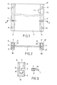
- a plate holder according to the invention is shown in plan view.
- a plate for example a Teflon or polyether sulfone plate laminated with copper on both sides and provided with conductor tracks, is arranged between two elongated and rod-shaped frame parts 2 and 2 'and inserted with the opposite edges into corresponding grooves 3 and 3', the depth of which is shown by the dashed lines is indicated within the frame parts 2, 2 '.
- Soldering channels 4 and 4 ' run from the top of the frame parts 2, 2' to the grooves 3, 3 'underneath and thereby connect them to the outside space.
- various types of fastening holes 14 can be provided in the frame parts 2, 2', which, in the form of continuous bores or threaded holes, serve to connect the frame parts 2, 2 'to a base and / or cover plates. Furthermore, it is possible to leave recesses 11 on the edge of the plate, which in connection with a corresponding through-bore 15 through the frame part 2 'has space for externally operable circuit elements, e.g. Trimmer, or power supply through feedthrough capacitors.
- circuit elements e.g. Trimmer
- FIG. 2 shows the cross section through a plate holder according to FIG. 1 in a plane identified by the line AA 'in FIG. 1.
- the frame parts 2, 2 typically have a prismatic cross section.
- the grooves 3, 3 ' run in the longitudinal direction on the frame inner sides 5, 5' and have a depth of several millimeters, which is sufficient on the one hand to give the plate 1 sufficient support and on the other hand does not take up an unnecessarily large area from the plate 1 takes. If the plate is a double sided printed.
- Printed circuit board is, which is equipped from the top and bottom with electronic components of a certain height, it is expedient that the grooves 3 and 3 'run in the central region of the frame inner sides 5, 5' to complete on both sides of the board Shielding housing to gain enough space.
- solder channels 4, 4 ' extend at least to the grooves 3, 3' from the frame tops 6, 6 ', but are closed towards the frame undersides 16 and 16', so that the liquid solder from the solder channels 4, 4 during the soldering process 'into the groove 3, 3', but cannot flow out downwards.
- the solder channels 4, 4' it is advantageous to design the solder channels 4, 4' as vertical blind holes to the plate 1, which extend through the groove 3, 3 'in depth if the soldering is to be carried out on both sides, and with them Central axes are arranged with respect to the groove depth such that they are only partially cut by the grooves. Such blind holes are very easy to make using automatic drills.
- a recess 11 at the edge of the plate, as shown in FIG. 1.
- a trimmer can be arranged lying, which is connected to the circuit by conductor tracks on the plate 1 is. Since such a recess 11 interrupts the continuous soldering of the plate edge 12 ', in this case 11 solder channels must be provided on both sides of the recess in order to supply the solder required for the soldering process on both sides.
- the frame parts 2, 2' have a surface which has excellent solderability with excellent electrical conductivity combined. This is achieved very advantageously and at the same time economically in that the frame parts are made of an inexpensive metal, e.g. Brass, are made and have a silver-plated surface.
- the soldered connection is then expediently imparted by a solder saturated with silver, which prevents silver from dissolving from the surface layer of the frame parts during the soldering process and impairing the quality of the soldered joint.
- the distribution of the liquid solder from the soldering channels 4, 4 'into the gap-shaped spaces formed on both sides of the plate edges between the grooves 3, 3' and the plate edges 12, 12 ' takes place by capillary forces and is therefore closely related to the geometric dimensions of the latter Spaces together. So that the capillary forces are effective but also the amount of solder required is kept low, it is advantageous that the width of the grooves 3, 3 'only exceeds the thickness of the plate edges 12, 12' in them by less than 0.2 mm. For example, if the thickness is 1.6 mm, excellent results with regard to the soldered connection are obtained with a groove width of 1.7 mm.
- the flow properties of the solder used and the geometric dimensions of frame parts 2, 2 ' and plate 1 determines the appropriate distribution of the various solder channels along the frame parts. If the solder from a solder channel penetrates only a few millimeters sideways into the gap between the frame part and the edge of the plate, the solder channels must be arranged in a correspondingly denser sequence than if the maximum propagation path is several centimeters. In the case of frame parts with a silver-plated surface and a groove depth of approximately 2.5 mm and when using a conventional soft solder, distances between adjacent solder channels of 10-30 mm have proven effective.
- Fig. 3 the cross section through a frame part 2 and the edge part of the plate 1 is shown on an enlarged scale before assembly.
- the groove inner surfaces 8 and 8 'are used which are opposite edge surfaces 7 and 7' in the inserted state.
- these edge surfaces 7, 7 'are copper layers with a width that is at least approximately as large as the groove depth and a surface that pretreated to improve the solderability, e.g. can be pre-tinned. It is particularly advantageous if the edge surfaces 7, 7 'are somewhat wider than the groove depth, because after the soldering process the quality of the soldering can then be checked optically using the visible soldering strip.
- the shielding of the circuit is completed in the manner shown in FIG. 4.
- the shielding housing is closed at the top and bottom by electrically conductive cover plates 9 and 9 ', which bear against the frame parts 2 and 2' with good electrical contact and are fastened to them.
- the lower cover plate 9 ' can also are replaced by the fact that the frame parts 2 and 2 ', with the soldered plate 1 in between, are scraped onto a larger, conductive carrier plate which takes over the lower part of the shield and also carries other plate holders of the same type.
- the transverse sides can be covered together with the open upper side if an upper cover plate 9 with angled and adapted side surfaces is used.
- the solder is filled into the soldering channels 4, 4'. This can be done in such a way that pieces of a solder wire of the required length and with a diameter not much smaller than that of the solder channel are inserted into the solder channel. When heated, the molten solder then fills the solder channel and spreads sideways along the groove from the solder channel.
- the frame parts are heated until the solder melts in the solder channels and flows into the groove. So that the flow process is not impaired by a very different temperature distribution in the frame parts 2, 2 ', the heating should take place as uniformly as possible over the entire length of the frame. This can be achieved with a soldering arrangement as shown in FIG. 5.
- the frame parts 2, 2 'with the inserted plate 1 are placed on a highly heat-conductive and dimensionally stable, flat base 19, which is heated from its underside with the necessary heat H and, due to its good thermal conductivity, distributes the temperature evenly.
- a plate holder according to the invention proves to be a mechanically stable and electrically reliable arrangement for a printed circuit board, which on the one hand requires a good earth connection and on the other hand has to be adequately shielded.
- a particular advantage of the holder is that it can be produced automatically in a simple manner.
Landscapes
- Engineering & Computer Science (AREA)
- Microelectronics & Electronic Packaging (AREA)
- Shielding Devices Or Components To Electric Or Magnetic Fields (AREA)
- Waveguide Aerials (AREA)
- Vehicle Step Arrangements And Article Storage (AREA)
- Casings For Electric Apparatus (AREA)
- Push-Button Switches (AREA)
- Reinforced Plastic Materials (AREA)
- Holding Or Fastening Of Disk On Rotational Shaft (AREA)
- Other Liquid Machine Or Engine Such As Wave Power Use (AREA)
- Table Devices Or Equipment (AREA)
- Adornments (AREA)
Priority Applications (1)
| Application Number | Priority Date | Filing Date | Title |
|---|---|---|---|
| AT84102492T ATE25913T1 (de) | 1983-03-25 | 1984-03-08 | Plattenhalterung, insbesondere fuer rfleiterplatten, sowie ein verfahren zu deren herstellung. |
Applications Claiming Priority (2)
| Application Number | Priority Date | Filing Date | Title |
|---|---|---|---|
| CH164983 | 1983-03-25 | ||
| CH1649/83 | 1983-03-25 |
Publications (2)
| Publication Number | Publication Date |
|---|---|
| EP0124712A1 true EP0124712A1 (fr) | 1984-11-14 |
| EP0124712B1 EP0124712B1 (fr) | 1987-03-11 |
Family
ID=4215391
Family Applications (1)
| Application Number | Title | Priority Date | Filing Date |
|---|---|---|---|
| EP84102492A Expired EP0124712B1 (fr) | 1983-03-25 | 1984-03-08 | Support de plaques, en particulier pour plaque à circuit RF et son procédé de fabrication |
Country Status (5)
| Country | Link |
|---|---|
| US (1) | US4609970A (fr) |
| EP (1) | EP0124712B1 (fr) |
| AT (1) | ATE25913T1 (fr) |
| DE (1) | DE3462652D1 (fr) |
| NO (1) | NO161770C (fr) |
Cited By (3)
| Publication number | Priority date | Publication date | Assignee | Title |
|---|---|---|---|---|
| EP0278382A3 (fr) * | 1987-02-06 | 1989-10-18 | Siemens Aktiengesellschaft Österreich | Filtre barrière |
| EP0381378A3 (fr) * | 1989-02-03 | 1992-01-08 | Nokia Mobile Phones Ltd. | Méthode de fabrication du châssis d'un radiotéléphone et châssis fabriqué selon cette méthode |
| EP0608718A3 (en) * | 1993-01-27 | 1996-01-10 | Siemens Nixdorf Inf Syst | Device for reducing stray radiation from flat assemblies. |
Families Citing this family (6)
| Publication number | Priority date | Publication date | Assignee | Title |
|---|---|---|---|---|
| US5244840A (en) * | 1989-05-23 | 1993-09-14 | Mitsubishi Denki Kabushiki Kaisha | Method for manufacturing an encapsulated IC card having a molded frame and a circuit board |
| SE468575B (sv) * | 1991-06-14 | 1993-02-08 | Ericsson Telefon Ab L M | Anordning med laminaera ledningsmoenster och valbara dielektrika |
| US5285353A (en) * | 1992-12-28 | 1994-02-08 | Delco Electronics Corporation | Support bar for circuit boards |
| FI119756B (fi) * | 1995-01-18 | 2009-03-13 | Alteon Inc | Tiatsoliumyhdisteiden käyttö pitkälle edenneen glykosylaation lopputuotteiden muodostumisen estossa ja suunnan muutoksessa |
| US20050014747A1 (en) * | 2003-04-18 | 2005-01-20 | Emily Reinhard | Dihydrothiazine prodrugs of thiazolium agents |
| JP6683670B2 (ja) * | 2017-11-21 | 2020-04-22 | ファナック株式会社 | ロック機構 |
Citations (4)
| Publication number | Priority date | Publication date | Assignee | Title |
|---|---|---|---|---|
| CH379211A (de) * | 1960-09-01 | 1964-06-30 | Sulzer Ag | Verbindung zweier zylindrischer metallischer Werkstücke durch Spaltlötung |
| GB1073108A (en) * | 1965-02-16 | 1967-06-21 | Siemens Ag | Improvements in or relating to the screening of printed circuit boards |
| FR2116630A5 (fr) * | 1970-12-01 | 1972-07-21 | Cit Alcatel | |
| GB2029645A (en) * | 1978-08-07 | 1980-03-19 | Mitsumi Electric Co Ltd | High-frequency circuit device |
Family Cites Families (4)
| Publication number | Priority date | Publication date | Assignee | Title |
|---|---|---|---|---|
| US3806767A (en) * | 1973-03-15 | 1974-04-23 | Tek Wave Inc | Interboard connector |
| FR2246154A1 (en) * | 1974-06-06 | 1975-04-25 | Precitec Gmbh | Grips for printed circuit boards - which can easily and rapidly be installed use sharp edged clips to dig into board |
| US3992653A (en) * | 1975-08-18 | 1976-11-16 | Sperry Rand Corporation | Zero insertion force card guide |
| US4517625A (en) * | 1983-11-09 | 1985-05-14 | Lockheed Corporation | Circuit board housing with zero insertion force connector |
-
1984
- 1984-03-08 AT AT84102492T patent/ATE25913T1/de not_active IP Right Cessation
- 1984-03-08 DE DE8484102492T patent/DE3462652D1/de not_active Expired
- 1984-03-08 EP EP84102492A patent/EP0124712B1/fr not_active Expired
- 1984-03-16 NO NO841047A patent/NO161770C/no unknown
- 1984-03-22 US US06/592,279 patent/US4609970A/en not_active Expired - Fee Related
Patent Citations (4)
| Publication number | Priority date | Publication date | Assignee | Title |
|---|---|---|---|---|
| CH379211A (de) * | 1960-09-01 | 1964-06-30 | Sulzer Ag | Verbindung zweier zylindrischer metallischer Werkstücke durch Spaltlötung |
| GB1073108A (en) * | 1965-02-16 | 1967-06-21 | Siemens Ag | Improvements in or relating to the screening of printed circuit boards |
| FR2116630A5 (fr) * | 1970-12-01 | 1972-07-21 | Cit Alcatel | |
| GB2029645A (en) * | 1978-08-07 | 1980-03-19 | Mitsumi Electric Co Ltd | High-frequency circuit device |
Cited By (3)
| Publication number | Priority date | Publication date | Assignee | Title |
|---|---|---|---|---|
| EP0278382A3 (fr) * | 1987-02-06 | 1989-10-18 | Siemens Aktiengesellschaft Österreich | Filtre barrière |
| EP0381378A3 (fr) * | 1989-02-03 | 1992-01-08 | Nokia Mobile Phones Ltd. | Méthode de fabrication du châssis d'un radiotéléphone et châssis fabriqué selon cette méthode |
| EP0608718A3 (en) * | 1993-01-27 | 1996-01-10 | Siemens Nixdorf Inf Syst | Device for reducing stray radiation from flat assemblies. |
Also Published As
| Publication number | Publication date |
|---|---|
| EP0124712B1 (fr) | 1987-03-11 |
| NO841047L (no) | 1984-09-26 |
| NO161770C (no) | 1989-09-20 |
| US4609970A (en) | 1986-09-02 |
| NO161770B (no) | 1989-06-12 |
| ATE25913T1 (de) | 1987-03-15 |
| DE3462652D1 (en) | 1987-04-16 |
Similar Documents
| Publication | Publication Date | Title |
|---|---|---|
| EP0920055B1 (fr) | Dispositif de refroidissement pour un composant générant de la chaleur sur un circuit imprimé | |
| DE3790315C2 (fr) | ||
| DE2532670C2 (fr) | ||
| DE4020498C2 (de) | Verfahren zum Herstellen von Multiwire-Leiterplatten mit isolierten Metalleitern und/oder optischen Leitern | |
| DE2037553C3 (de) | Rücklötbare Anschlußverbindung | |
| DE19634202C2 (de) | Halbleitervorrichtung | |
| DE4203605A1 (de) | Elektrischer verbinder | |
| DE3535923A1 (de) | Substrathaltender aufbau | |
| DE2103064A1 (de) | Vorrichtung zur Herstellung von Modulelementen | |
| EP0124712B1 (fr) | Support de plaques, en particulier pour plaque à circuit RF et son procédé de fabrication | |
| DE3149236C2 (de) | Schweißwerkzeug | |
| DE2639979B2 (de) | Halbleiterbaueinheit | |
| DE69838604T2 (de) | Gedruckte platte und verfahren zu deren herstellung | |
| DE3525012A1 (de) | Busleiste fuer die oberflaechenmontage | |
| DE10001180B4 (de) | Doppelseitenmuster-Verbindungskomponente, gedruckte Schaltungsplatte und Verfahren zum Verbinden von auf beiden Seiten einer gedruckten Schaltungsplatte gebildeten Verbindungsmustern | |
| DE3902998C2 (fr) | ||
| DE3143339C2 (de) | Halbleiteranordnung | |
| DE10064221B4 (de) | Leiterplatine mit gekühltem SMD-Baustein | |
| EP0166817B1 (fr) | Méthode et dispositif pour braser des sorties d'éléments électriques aussi bien qu'un arrangement d'éléments électriques | |
| DE3323830C2 (de) | Anordnung zum Auflöten einer elektrischen Schaltungsplatte auf einen Grundkörper | |
| DE1059988B (de) | Elektrische Baugruppe | |
| DE1927387A1 (de) | Sonnenbatterie | |
| EP0204379B1 (fr) | Procédé de fabrication d'un boîtier hermétiquement fermé pour composants, en particulier pour résonateur en quartz | |
| EP0651598B1 (fr) | Module de circuit électronique | |
| DE4008658C2 (fr) |
Legal Events
| Date | Code | Title | Description |
|---|---|---|---|
| PUAI | Public reference made under article 153(3) epc to a published international application that has entered the european phase |
Free format text: ORIGINAL CODE: 0009012 |
|
| AK | Designated contracting states |
Designated state(s): AT CH DE GB LI |
|
| 17P | Request for examination filed |
Effective date: 19840914 |
|
| GRAA | (expected) grant |
Free format text: ORIGINAL CODE: 0009210 |
|
| AK | Designated contracting states |
Kind code of ref document: B1 Designated state(s): AT CH DE GB LI |
|
| REF | Corresponds to: |
Ref document number: 25913 Country of ref document: AT Date of ref document: 19870315 Kind code of ref document: T |
|
| REF | Corresponds to: |
Ref document number: 3462652 Country of ref document: DE Date of ref document: 19870416 |
|
| RAP2 | Party data changed (patent owner data changed or rights of a patent transferred) |
Owner name: BBC BROWN BOVERI AG |
|
| PLBE | No opposition filed within time limit |
Free format text: ORIGINAL CODE: 0009261 |
|
| STAA | Information on the status of an ep patent application or granted ep patent |
Free format text: STATUS: NO OPPOSITION FILED WITHIN TIME LIMIT |
|
| 26N | No opposition filed | ||
| PGFP | Annual fee paid to national office [announced via postgrant information from national office to epo] |
Ref country code: GB Payment date: 19890228 Year of fee payment: 6 |
|
| PGFP | Annual fee paid to national office [announced via postgrant information from national office to epo] |
Ref country code: AT Payment date: 19890302 Year of fee payment: 6 |
|
| PGFP | Annual fee paid to national office [announced via postgrant information from national office to epo] |
Ref country code: DE Payment date: 19890526 Year of fee payment: 6 |
|
| PGFP | Annual fee paid to national office [announced via postgrant information from national office to epo] |
Ref country code: CH Payment date: 19890626 Year of fee payment: 6 |
|
| PG25 | Lapsed in a contracting state [announced via postgrant information from national office to epo] |
Ref country code: GB Effective date: 19900308 Ref country code: AT Effective date: 19900308 |
|
| PG25 | Lapsed in a contracting state [announced via postgrant information from national office to epo] |
Ref country code: LI Effective date: 19900331 Ref country code: CH Effective date: 19900331 |
|
| GBPC | Gb: european patent ceased through non-payment of renewal fee | ||
| REG | Reference to a national code |
Ref country code: CH Ref legal event code: PL |
|
| PG25 | Lapsed in a contracting state [announced via postgrant information from national office to epo] |
Ref country code: DE Effective date: 19901201 |