EP0124719A1 - Stromtyp-GTO-Inverter - Google Patents
Stromtyp-GTO-Inverter Download PDFInfo
- Publication number
- EP0124719A1 EP0124719A1 EP84102580A EP84102580A EP0124719A1 EP 0124719 A1 EP0124719 A1 EP 0124719A1 EP 84102580 A EP84102580 A EP 84102580A EP 84102580 A EP84102580 A EP 84102580A EP 0124719 A1 EP0124719 A1 EP 0124719A1
- Authority
- EP
- European Patent Office
- Prior art keywords
- capacitor
- inverter
- reactor
- surge voltage
- thyristor
- Prior art date
- Legal status (The legal status is an assumption and is not a legal conclusion. Google has not performed a legal analysis and makes no representation as to the accuracy of the status listed.)
- Granted
Links
- 239000003990 capacitor Substances 0.000 claims abstract description 140
- 238000004804 winding Methods 0.000 claims description 53
- 230000001052 transient effect Effects 0.000 claims description 18
- 230000006698 induction Effects 0.000 claims description 12
- 230000001186 cumulative effect Effects 0.000 claims description 8
- 238000000034 method Methods 0.000 claims description 2
- 230000001939 inductive effect Effects 0.000 abstract description 4
- 230000001172 regenerating effect Effects 0.000 description 7
- 230000002441 reversible effect Effects 0.000 description 7
- 238000010586 diagram Methods 0.000 description 3
- 230000008929 regeneration Effects 0.000 description 3
- 238000011069 regeneration method Methods 0.000 description 3
- 230000004044 response Effects 0.000 description 3
- 238000010521 absorption reaction Methods 0.000 description 2
- 230000000903 blocking effect Effects 0.000 description 2
- 230000007423 decrease Effects 0.000 description 2
- 230000000694 effects Effects 0.000 description 2
- 238000009499 grossing Methods 0.000 description 2
- 238000004891 communication Methods 0.000 description 1
- 230000003247 decreasing effect Effects 0.000 description 1
- 230000003111 delayed effect Effects 0.000 description 1
- 230000001419 dependent effect Effects 0.000 description 1
- 230000004907 flux Effects 0.000 description 1
- 238000012986 modification Methods 0.000 description 1
- 230000004048 modification Effects 0.000 description 1
- 230000026683 transduction Effects 0.000 description 1
- 238000010361 transduction Methods 0.000 description 1
Images


Classifications
-
- H—ELECTRICITY
- H02—GENERATION; CONVERSION OR DISTRIBUTION OF ELECTRIC POWER
- H02M—APPARATUS FOR CONVERSION BETWEEN AC AND AC, BETWEEN AC AND DC, OR BETWEEN DC AND DC, AND FOR USE WITH MAINS OR SIMILAR POWER SUPPLY SYSTEMS; CONVERSION OF DC OR AC INPUT POWER INTO SURGE OUTPUT POWER; CONTROL OR REGULATION THEREOF
- H02M5/00—Conversion of AC power input into AC power output, e.g. for change of voltage, for change of frequency, for change of number of phases
- H02M5/40—Conversion of AC power input into AC power output, e.g. for change of voltage, for change of frequency, for change of number of phases with intermediate conversion into DC
- H02M5/42—Conversion of AC power input into AC power output, e.g. for change of voltage, for change of frequency, for change of number of phases with intermediate conversion into DC by static converters
- H02M5/44—Conversion of AC power input into AC power output, e.g. for change of voltage, for change of frequency, for change of number of phases with intermediate conversion into DC by static converters using discharge tubes or semiconductor devices to convert the intermediate DC into AC
- H02M5/443—Conversion of AC power input into AC power output, e.g. for change of voltage, for change of frequency, for change of number of phases with intermediate conversion into DC by static converters using discharge tubes or semiconductor devices to convert the intermediate DC into AC using devices of a thyratron or thyristor type requiring extinguishing means
- H02M5/45—Conversion of AC power input into AC power output, e.g. for change of voltage, for change of frequency, for change of number of phases with intermediate conversion into DC by static converters using discharge tubes or semiconductor devices to convert the intermediate DC into AC using devices of a thyratron or thyristor type requiring extinguishing means using semiconductor devices only
- H02M5/4505—Conversion of AC power input into AC power output, e.g. for change of voltage, for change of frequency, for change of number of phases with intermediate conversion into DC by static converters using discharge tubes or semiconductor devices to convert the intermediate DC into AC using devices of a thyratron or thyristor type requiring extinguishing means using semiconductor devices only having a rectifier with controlled elements
-
- H—ELECTRICITY
- H02—GENERATION; CONVERSION OR DISTRIBUTION OF ELECTRIC POWER
- H02M—APPARATUS FOR CONVERSION BETWEEN AC AND AC, BETWEEN AC AND DC, OR BETWEEN DC AND DC, AND FOR USE WITH MAINS OR SIMILAR POWER SUPPLY SYSTEMS; CONVERSION OF DC OR AC INPUT POWER INTO SURGE OUTPUT POWER; CONTROL OR REGULATION THEREOF
- H02M7/00—Conversion of AC power input into DC power output; Conversion of DC power input into AC power output
- H02M7/42—Conversion of DC power input into AC power output without possibility of reversal
- H02M7/44—Conversion of DC power input into AC power output without possibility of reversal by static converters
- H02M7/48—Conversion of DC power input into AC power output without possibility of reversal by static converters using discharge tubes with control electrode or semiconductor devices with control electrode
- H02M7/505—Conversion of DC power input into AC power output without possibility of reversal by static converters using discharge tubes with control electrode or semiconductor devices with control electrode using devices of a thyratron or thyristor type requiring extinguishing means
- H02M7/515—Conversion of DC power input into AC power output without possibility of reversal by static converters using discharge tubes with control electrode or semiconductor devices with control electrode using devices of a thyratron or thyristor type requiring extinguishing means using semiconductor devices only
- H02M7/5152—Conversion of DC power input into AC power output without possibility of reversal by static converters using discharge tubes with control electrode or semiconductor devices with control electrode using devices of a thyratron or thyristor type requiring extinguishing means using semiconductor devices only with separate extinguishing means
-
- H—ELECTRICITY
- H02—GENERATION; CONVERSION OR DISTRIBUTION OF ELECTRIC POWER
- H02M—APPARATUS FOR CONVERSION BETWEEN AC AND AC, BETWEEN AC AND DC, OR BETWEEN DC AND DC, AND FOR USE WITH MAINS OR SIMILAR POWER SUPPLY SYSTEMS; CONVERSION OF DC OR AC INPUT POWER INTO SURGE OUTPUT POWER; CONTROL OR REGULATION THEREOF
- H02M7/00—Conversion of AC power input into DC power output; Conversion of DC power input into AC power output
- H02M7/66—Conversion of AC power input into DC power output; Conversion of DC power input into AC power output with possibility of reversal
- H02M7/68—Conversion of AC power input into DC power output; Conversion of DC power input into AC power output with possibility of reversal by static converters
- H02M7/72—Conversion of AC power input into DC power output; Conversion of DC power input into AC power output with possibility of reversal by static converters using discharge tubes with control electrode or semiconductor devices with control electrode
- H02M7/75—Conversion of AC power input into DC power output; Conversion of DC power input into AC power output with possibility of reversal by static converters using discharge tubes with control electrode or semiconductor devices with control electrode using devices of a thyratron or thyristor type requiring extinguishing means
- H02M7/757—Conversion of AC power input into DC power output; Conversion of DC power input into AC power output with possibility of reversal by static converters using discharge tubes with control electrode or semiconductor devices with control electrode using devices of a thyratron or thyristor type requiring extinguishing means using semiconductor devices only
Definitions
- the present invention relates generally to a current type GTO (gate turn-off thyristor) inverter, and more specifically to a surge voltage clamping circuit for clamping the surge voltage generated when each GTO incorporated in a current type GTO bridge-connected inverter is turned off.
- the clamped surge voltage is stored once in a capacitor and then returned to the terminals between the rectifier and the GTO inverter for energy restoration.
- GTOs gate turn-off thyristors
- the terminology "commutation” means that the load current of one phase is switched to that. of another phase or vice versa by thyristor switching operation.
- a surge voltage clamping circuit for a current type GTO inverter comprises (a) a diode bridge-connected commutation surge voltage rectifier, (b) a capacitor for storing commutation surge voltage energy, (c) a cumulative reactor, (d) a first gate turn-off thyristor, (e) a second gate turn-off thyristor, (f) a first diode, (g) a second diode, and (h) a DC reactor.
- the commutation surge voltage energy stored in the capacitor is restored to the DC source terminals of the GTO inverter through the first and second gate turn-off thyristors when the charged-up capacitor voltage exceeds a predetermined value beyond the DC source voltage, and additionally the magnetic energy stored in the reactor is recharged to the capacitor through the first and second diodes after the two gate turn-off thyristors have been turned off.
- the method of restoring the commutation surge voltage to the DC source terminals of the GTO inverter comprising the following steps of:
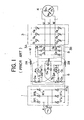
- the GTO inverter provided with a surge voltage clamping circuit is roughly made up of a thyristor bridge-connected current rectifier 1, a DC reactor having two .inductive reactances 2A and 2B magnetically connected each other, a GTO (gate turn-off thyristor) bridge-connected inverter 3, an induction motor 4, a diode bridge-connected commutation surge voltage rectifier 5, and a commutation surge voltage clamping circuit 6 including an electrolytic capacitor C l .
- the above clamping circuit 6 functions also as a commutation surge voltage energy restoring circuit.
- the thyristor bridge-connected rectifier 1 includes six rectifying thyristors RT 1 to RT 6 , which are turned on sequentially in the order of RT 1 and RT6, RT 3 and RT 2 and RT 5 and RT 4 so that each half cycle of the sine wave of a three-phase power source can be passed in sequence. Therefore, when the rectifying thyristors RT 2 and RT 6 are both turned on, a first-phase current is supplied from the terminal A to the terminal C by way of thyristor RT 1 , reactor 2A, terminal 3A, GTO bridge-connected inverter 3, motor 4, GTO bridge-connected inverter 3, terminal 3B, reactor 2B, and thyristor RT 6 .
- a second-phase current is supplied from the terminal B to the terminal A by way of rectifying thyristor RT 3 , reactor 2A, terminal 3A, GTO bridge-connected inverter 3, motor 4, GTO bridge-connected inverter 3, terminal 3B, reactor 2B and the rectifying thyristor RT 2 ;
- a third phase current is supplied from the terminal C to the terminal B by way of the rectifying thyristor RT 5 , reactor 2A, terminal 3A, GTO bridge-connected inverter 3, motor 4, GTO bridge-connected inverter 3, terminal 3B, reactor 2B, and rectifying thyristor RT 4 .
- the rectified full-wave direct current is further smoothed through the DC cumulative reactor having two inductances 2A and 2B magnetically connected each other. Therefore, the smoothed direct current Id is further converted into an alternate current of an appropriate frequency through the GTO inverter 3 to drive the induction motor 4 at any desired speed.
- the GTO inverter 3 includes six bridge-connected GTOs G1 to G 6 .
- GTOs When the GTOs are turned on in the order of G 1 and G 6 and then G 3 with G 6 on in sequence for each 60 degrees, an alternate square-wave U-phase current i with a pulse width of 60 degrees is first obtained by the GTO inverter.
- GTOs When the GTOs are turned on in the order of G 3 and G 6 and then G 2 with G 3 on in sequence for each 60 degrees, an alternate square-wave V-phase current i v with a pulse width of 120 degrees is obtained by the GTO inverter.
- GTO inverter When the GTOs are turned on in the order of G 3 and G 2 and then G 5 with G 2 on in sequence for each 60 degrees, an alternate square-wave W-phase current i w with a pulse width of 120 degrees is obtained by the GTO inverter.
- the rectified direct current Id flows as the U-phase current (the latter half of 120 degrees) i u through the first U-phase winding having reactance X u and the third W-phase winding having reactance X w of.the motor.
- the current Id flows as the V-phase current (the first half of 120 degrees) i through the second V-phase winding having reactance X v and the third W-phase winding having reactance X .
- the current Id flows as the V-phase current (the latter half of 120 degrees) i v through X v and X u .
- the current Id flows as the W-phase current (the first half of 120 degrees) i w through X W and X u .
- GTOs are turned off in the order of G 1 , G 6 , G 3 , G 2 , G 5 and G 4 for each 60 degrees.
- the current passed through these three-phase windings having motor reactances X u , X v , and X w generates a rotational magnetic flux.
- a surge voltage clamping circuit including a diode bridge-connected commutation surge voltage rectifying section 5 made up of fix diodes D 1 to D 6 and a surge voltage clamping section 6 made u p of an electrolytic capacitor C 1 ,two capacitors C 2 and C 31 two ordinary thyristors T 1 and T 2 , four diodes D 8 to D 11 , two turning-off indictors L 1 and L 2 , and a reactor having two reactances Lr 1 and Lr 2 , as shown in Fig. 1.
- the positive side of the first reactance Lr 1 is connected to the positive terminal of the DC rectifier 1 through the diode D 10 ; the negative side of the second reactance Lr 2 is connected to the negative terminal of the DC rectifier through the diode D 11 , respectively.
- mode I When mode I (G 1 and G 6 are on) is switched to mode II ( G1 is off, G6 is on, G 3 is on), for instance, as depicted in Fig. 2, the current i u flowing through windings X u and X w is commutated to the current i v flowing through windings X and X w .
- the current i u does not immediately fall to zero level but decreases gradually and the current i v does not immediately rise to the current Id but increases gradually as depicted in Fig. 2. This is because there exists each inductance in each winding and thereby an induced surge voltage is inevitably generated across each winding. It is very important to suppress or eliminate these induced surge voltages for protection of GTO thyristors.
- An induced surge voltage V vw developed across the windings X v and X w in this transient state can be charged in the capacitor C 1 as follows:
- the surge voltage V vw exceeds the voltage across the capacitor C 1 , since the diodes D 3 and D 6 are both forward biased (the anode of D 3 is high in voltage level; the cathode of D 6 is low in voltage level), the major part of the current to be passed through the winding X v flows by way of GTO G 3 , diode D 3 , capacitor C l , diode D 6 and GTO G 6 .
- the surge voltage V vw is suppressed by the capacitor C 1 if the voltage e cl across the capacitor C 1 is sufficiently low.
- the induced surge voltage V wu developed across the windings X w and X u becomes zero as shown in Fig. 2.
- the current i v increases gradually up to the direct current Id in accordance with a time constant determined by the circuit constant of the motor load.
- the diode D 2 is cut off.
- no induced surge voltage is generated in the winding X u .
- the diodes D 3 and D 6 are both cut off, so that the capacitor C 1 is electrically disconnected from the inverter 3 and thus the commutation from GTO G 1 to GTO G 3 is completed.
- the above-mentioned mode II corresponds to the overlapped (transient) period in a series-connected diode type current inverter.
- the GTO inverter shown in Fig. 1 and the series-connected diode type current inverter in that two transient currents flow through the each-phase winding in the directions opposite to each other being superimposed upon each other.
- the two reverse blocking ordinary thyristors T 1 and T 2 are turned on in response to a pulse applied to each gate terminal thereof. Therefore, the surge voltage energy stored in the capacitor C1 is discharged to the DC source terminals 3A and 3B of the GTO inverter 3 by way of inductor L 1 , thyristor T 1 , reactor Lr 1 , diode D 10 , reactor 2A, GTO inverter 3, motor 4, GTO inverter 3, reactor 2B, diode D 11 , reactor Lr 2 , thyristor T 2 , and inductor L 2 .
- the above-mentioned discharge is called commutation surge voltage energy restoration or energy rebound.
- the capacitors C 2 and C 3 are also charged up with the polarity as shown in Fig. 1.
- These two capacitors C 2 and C 3 form two vibration circuits independently.
- the first vibration circuit is made up of the capacitor C 2 .and the inductor L 1 ;
- the second vibration circuit is made up of the capacitor C 3 and the inductor L 2 , each having a relatively high frequency or a relatively small time constant.
- An example of the voltage wave form ec2 or e c3 across the capacitor C 2 or C 3 is also shown in Fig. 2.
- the thyristor T 1 or T 2 is automatically turned off, because a positive potential is applied to the anode of the thyristor T l or T 2 .
- the polarity of the charged-up voltages of the three capacitors C 1 , C 2 , C 3 are the same, that is, three charged-up voltages are added to each other.
- the inductance Lr 1 or Lr 2 of the reactor is so determined as to be sufficiently greater than that of the turning-off (vibration) inductor L 1 or L 2 , the two vibration circuits L 1 ⁇ C 2 and L 2 .C 3 can stably vibrate and provide an sufficient turn-off time for the thyristor T 1 or T 2 .
- the reactor Lr 1 or Lr 2 functions as a smoothing element.
- the operation mode shifts to the mode III in which the driving current is supplied from GTO G 3 , through windings X v and X w , to GTO G 6 .
- GTOs are incorporated in the surge voltage clamping circuit, without providing turning-off (vibration) circuit, in order to oeprate the circuit stably at a high speed.
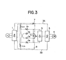
- a single direct-current reactor 7 is incorporated in place of the cumulative direct-current reactors 2A and 2B and (2) two gate turn-off thyristors (GTOs) G 7 and G 8 are incorporated without providing the vibration circuits including two inductors L 1 and L 2 and capacitors C 2 and C 3 .
- GTOs gate turn-off thyristors
- a surge voltage clamping circuit 8 or a surge energy restoring circuit comprises an electrolytic capacitor C 1 for absorbing the commutation surge voltage energy, two GTOs G 7 and G 8 for restoring the surge voltage energy stored in the capacitor C 1 to the GTO inverter 3, a cumulative reactor having two inductive reactances Lr 1 and Lr 2 magnetically connected to each other for smoothing the current restored from the capacitor C 1 to the GTO inverter 3, and two diodes D 8 and D 9 for storing the magnetic energy stored in the reactor Lr 1 , Lr 2 to the capacitor C1 after the surge voltage energy stored in the capacitor C 1 has been restored.
- the electrolytic capacitor C 1 is connected in parallel with the diode bridge-connected commutation surge voltage rectifier 5.
- the two GTOs are connected between the reactor Lr 1 and Lr 2 and the capacitor C 1 as follows:
- the positive side of the first winding Lr 1 is connected to the positive terminal of the DC source;
- the negative side of the first winding Lr 1 is connected to the cathode of the first GTO G 7 ;
- the anode of the first GTO G 7 is connected to the positive side of the capacitor C 1 ;
- the negative side of the second winding Lr 2 is connected to the negative terminal of the DC source;
- the positive side of the second winding Lr 2 is connected to the anode of the second GTO G 8 ;
- the cathode of the second GTO G 8 is connected to the negative side of the capacitor C 1 , respectively, respectively.
- the two diodes D 8 and D 9 are connected between the reactor Lr 1 and Lr 2 and the capacitor C 1 as follows: the cathode of the first diode D 8 is connected to the positive side of the capacitor C 1 ; the anode of the first diode D 8 is connected to the positive side of the second winding Lr 2 ; the cathode of the second diode D 9 is connected to the negative side of the first winding Lr 1 and the anode of the second diode D 9 is connected to the negative side of the capacitor C 1 .
- the GTOs G 7 and G 8 are turned on when the voltage e cl developed across the capacitor C 1 exceeds a predetermined value beyond the DC source voltage developed across the thyristor bridge rectifier 1. Therefore, the GTOs G 7 and G 8 are not turned on whenever the GTO inverter 3 is commutated, being different from the prior-art surge voltage clamping circuit shown in Fig. 1. In other words, the energy stored in the capacitor C1 is restored or regenerated without synchronization with the commutation of the GTO inverter 3.
- the surge voltage clamping circuit 8 When surge voltage is generated by the commutation of the GTO inverter 3, the surge voltage energy is charged into the electrolytic capacitor C1 through the diode bridge rectifier 5 with the polarity as shown in Fig. 3. If the voltage level of the capacitor C1 exceeds a predetermined value beyond the DC voltage of the thyristor bridge rectifier 1, the GTOs G 7 and G 8 are turned on by a gate circuit (not shown).
- the surge voltage energy stored in the capacitor C 1 is restored to the DC source terminals 3A and 3B of the GTO inverter 3 by way of GTO G 7 , first winding Lr 1 , DC reactor 7, GTO inverter 3, motor 4, GTO inverter 3, second winding Lr 2 , and GTO G 8 .
- the gate circuit turns off the GTOs G 7 and G 8 simultaneously.
- the magnetic energy stored in the first and second windings Lr 1 and Lr 2 is supplied to the capacitor C 1 to charge it by way of second winding Lr 2 , diode D 8 , capacitor C 1 , diode D 9 and first winding Lr 1 in the forward direction of the two diodes D 8 and D 9 .
- the surge voltage clamping circuit 8 has the following features:
- the motor torque T is positive and the rotor angular frequency ⁇ r also is positive; in the second quadrant, T is negative but ⁇ r is positive; in the third quadrant, T is negative and ⁇ r is also negative; in the fourth quadrant, T is positive but ⁇ r is negative, as depicted in Fig. 4B.
- Fig. 4C shows an example in which a motor rotating in the normal direction is switched to the reverse direction at time t l .
- a motor when a motor is rotating in the 1st quadrant operation (T>0, ⁇ r >0), if the reference frequency (speed) +w* is switched to - ⁇ * r , the motor rotates in the 2nd quadrant operation (T ⁇ 0, ⁇ r >0) (the motor is braked or the motor torque is absorbed). The instant the rotor frequency reaches zero, the motor begins to rotate in the 3rd quadrant operation (T ⁇ 0, ⁇ r ⁇ 0) (the motor is driven in the reverse direction).
- the induction motor While the induction motor is being braked for stopping the motor or for reversing the rotational direction of the motor, the induction motor operates as a generator which can return the motor rotational kinetic energy to the AC source side.
- a first pair of GTOs 7 and 8 are used for restoring the load inductive power (magnetic energy) to the DC source terminals of the GTO inverter 3 as in the first embodiment shown in Fig. 3 and a second pair of GTOs 9 and 10 are additionally used for regenerating the motor kinetic energy produced in motor braking operation to the AC source side.
- the electrolytic capacitor C l is connected in parallel with the diode bridge-connected communication surge voltage rectifier 5 as in the first embodiment shown in Fig. 3.
- An additional pair of GTOs G 9 and G 10 for regenerating the motor rotational energy produced in motor braking operation to the AC source side are connected between the reactor Lr 1 and Lr 2 and the capacitor C 1 as follows: the anode of the third GTO G 9 is connected to the positive side of the capacitor C l ; the cathode of the third GTO G 9 is connected to the positive side of the second winding Lr 2 , the anode of the fourth GTO G 10 is connected to the negative side of the first winding Lr l ; the cathode of the fourth GTO G 10 is connected to the negative side of the capacitor C lo
- an additional pair of diodes D 12 and D 13 are connected between the reactor Lr 1 and Lr 2 and the capacitor C 1 as follows: the anode of the third diode D 12 is connected to the negative side of the first winding Lr l ; the cathode of the third diode D 12 is connected to the positive side of the capacitor C l ; the anode of the fourth diode D 13 is connected to the negative side of the capacitor C l ; and the cathode of the fourth diode D 13 is connected to the positive side of the second winding Lr 2 .
- the GTOs G 7 and G 8 are referred to as in-drive energy restoring GTOs; the GTOs G 9 and G 10 are referred to as in-brake energy regenerating GTOs; the diodes D 8 and D 9 are referred to as in-drive energy restoring diodes; the diodes D 12 and D 13 are referred to as in-brake energy regenerating diodes, hereinafter.
- the above-mentioned energy restoring GTOs G 7 and G 8 and energy regenerating GTOs G 9 and G 10 are turned on only in the steady state but turned off in the transient state, in response to each gate signal generated by each gate circuit (not shown), in order to realize the energy restoration or regeneration function.
- the surge voltage energy is charged into the capacitor C 1 from the inverter 3 through the diode bridge-connected rectifier 5.
- the energy restoring GTOs G 7 and G 8 are turned on in the steady state interval, the energy stored in the capacitor C 1 is discharged (restored) to the DC source terminals 3A and 3B of the GTO inverter 3 by way of capacitor C l , GTO G 7 , reactor Lr 1 , reactor 7, GTO inverter 3, motor 4, GTO inverter 3, reactor Lr 2 , GTO G 8 , and capacitor C 1 .
- the magnetic energy stored in the reactor Lr 1 , Lr 2 is recharged into the capacitor C 1 by way of reactor Lr 2 , diode D 8 , capacitor C 1 , diode D 9 , reactor Lr 1 as in the first embodiment shown in Fig. 3.
- the current flows through the reactor Lr in a predetermined direction.
- the energy regenerating GTOs G 9 , G 10 can be turned on, so that the energy charged in the capacitor C 1 is regenerated to the AC source side by way of capacitor C 1 , GTO G 9 , reactor Lr 2 , the thyristor bridge-connected current rectifier 1, reactor Lr 1 , GTO G 10 and capacitor C 1 .
- the diodes D 12 and D 13 are reversely biased.
- the GTOs G 9 , G 10 are turned on in the steady state interval and off in the transient state interval.
- the capacitor C 1 since the regeneration energy in motor braking operation becomes great in a moment and therefore the capacitor C 1 is immediately charged up, it is preferable to predetermine the discharge time interval of the capacitor C 1 to be long without distinction of the transient state interval and the steady state interval. That is to say, it is preferable to turn on the GTO G 9 and G 10 whenever the voltage e cl across the capacitor C 1 exceeds a predetermined reference value.
- the surge voltage clamping circuit of the present invention provides the first function to absorb the surge voltage energy generated in the transient state interval (commutation period), the second function to restore the surge voltage energy to the DC source terminal of the GTO inverter in the steady state interval, and the third function to regenerate the motor kinetic energy to the AC source side in brake state interval.
- the above surge voltage absorbing function is greatly dependent upon the voltage e cl developed across the capacitor C 1 .
- This voltage e cl can be controlled by changing the off-time interval of the GTOs G 7 and G 8 . If the DC source voltage and its frequency of the GTO inverter 3 are determined to be constant, the longer the off-time interval of G 7 and G 8 , the higher the voltage e cl because the discharge interval of capacitor C 1 decreases. If the DC source voltage and the off-time interval are determined to be constant, the higher the DC source voltage frequency, the higher the voltage e cl because the surge energy for a predetermined time interval increases.
- the surge voltage clamping circuit for a current-type GTO inverter since there is provided an additional function to regenerate the motor kinetic energy to the AC source side when the motor is being braked, it is possible to further improve the energy transduction efficiency of a current-type GTO inverter and additionally to readily drive or brake an induction motor in order to enable the four-quadrant operation.
Landscapes
- Engineering & Computer Science (AREA)
- Power Engineering (AREA)
- Inverter Devices (AREA)
- Control Of Ac Motors In General (AREA)
- Power Conversion In General (AREA)
- Protection Of Static Devices (AREA)
Applications Claiming Priority (2)
| Application Number | Priority Date | Filing Date | Title |
|---|---|---|---|
| JP40096/83 | 1983-03-11 | ||
| JP58040096A JPS59165970A (ja) | 1983-03-11 | 1983-03-11 | 電流形gtoインバ−タの電圧クランプ回路 |
Publications (2)
| Publication Number | Publication Date |
|---|---|
| EP0124719A1 true EP0124719A1 (de) | 1984-11-14 |
| EP0124719B1 EP0124719B1 (de) | 1987-08-12 |
Family
ID=12571339
Family Applications (1)
| Application Number | Title | Priority Date | Filing Date |
|---|---|---|---|
| EP84102580A Expired EP0124719B1 (de) | 1983-03-11 | 1984-03-09 | Stromtyp-GTO-Inverter |
Country Status (5)
| Country | Link |
|---|---|
| US (1) | US4580205A (de) |
| EP (1) | EP0124719B1 (de) |
| JP (1) | JPS59165970A (de) |
| KR (1) | KR890003301B1 (de) |
| DE (1) | DE3465396D1 (de) |
Cited By (1)
| Publication number | Priority date | Publication date | Assignee | Title |
|---|---|---|---|---|
| EP0234293A3 (en) * | 1986-01-24 | 1988-09-28 | Kabushiki Kaisha Meidensha | Reactive power processing circuit for a current source gto invertor |
Families Citing this family (7)
| Publication number | Priority date | Publication date | Assignee | Title |
|---|---|---|---|---|
| US5400235A (en) * | 1992-08-07 | 1995-03-21 | International Business Machines Corp. | High frequency energy saving DC to DC power converter |
| DE19539573A1 (de) * | 1995-10-25 | 1997-04-30 | Asea Brown Boveri | Summenlöschkreis für einen Thyristor-Stromrichter |
| FR2742013B1 (fr) * | 1995-11-30 | 1998-03-27 | Sgs Thomson Microelectronics | Procede et dispositif de limitation d'appel de courant d'un condensateur associe a un redresseur |
| KR100433954B1 (ko) * | 1999-08-04 | 2004-06-04 | 주식회사 포스코 | 쓰리 레벨 지티오 인버터/컨버터용 스너버 회로 |
| JP5569204B2 (ja) | 2010-07-13 | 2014-08-13 | サンケン電気株式会社 | 共振型インバータ装置 |
| US11056984B2 (en) * | 2017-09-29 | 2021-07-06 | Aisin Aw Co., Ltd. | Inverter control device |
| EP4415250B1 (de) | 2023-02-09 | 2025-11-26 | GE Energy Power Conversion Technology Ltd | Schaltmodul einer elektronischen leistungsschaltanordnung und verfahren zu dessen kommutierung |
Citations (2)
| Publication number | Priority date | Publication date | Assignee | Title |
|---|---|---|---|---|
| US3887862A (en) * | 1972-09-22 | 1975-06-03 | Siemens Ag | Auxiliary extinguishing arrangement for the inverters in an intermediate link converter |
| GB1429880A (en) * | 1972-07-03 | 1976-03-31 | Jeumont Schneider | System for adjusting and commutating current in machine windings |
Family Cites Families (4)
| Publication number | Priority date | Publication date | Assignee | Title |
|---|---|---|---|---|
| FR2315193A1 (fr) * | 1975-06-16 | 1977-01-14 | Jeumont Schneider | Convertisseur de courant a frequence variable pour l'alimentation d'une machine a courant alternatif |
| JPS52144738A (en) * | 1976-05-27 | 1977-12-02 | Mitsubishi Electric Corp | Surge absorber circuit for power convertor |
| US4309751A (en) * | 1978-12-25 | 1982-01-05 | Tokyo Shibaura Denki Kabushiki Kaisha | Method and apparatus for controlling current type inverters |
| JPS5863082A (ja) * | 1981-10-09 | 1983-04-14 | Fanuc Ltd | インバータ装置 |
-
1983
- 1983-03-11 JP JP58040096A patent/JPS59165970A/ja active Granted
-
1984
- 1984-03-08 US US06/587,642 patent/US4580205A/en not_active Expired - Fee Related
- 1984-03-09 DE DE8484102580T patent/DE3465396D1/de not_active Expired
- 1984-03-09 EP EP84102580A patent/EP0124719B1/de not_active Expired
- 1984-03-10 KR KR1019840001224A patent/KR890003301B1/ko not_active Expired
Patent Citations (2)
| Publication number | Priority date | Publication date | Assignee | Title |
|---|---|---|---|---|
| GB1429880A (en) * | 1972-07-03 | 1976-03-31 | Jeumont Schneider | System for adjusting and commutating current in machine windings |
| US3887862A (en) * | 1972-09-22 | 1975-06-03 | Siemens Ag | Auxiliary extinguishing arrangement for the inverters in an intermediate link converter |
Non-Patent Citations (1)
| Title |
|---|
| Patent Abstracts of Japan vol. 2, no. 23, 15 February 1978 page 11720E77 & JP-A-52-144738 * |
Cited By (1)
| Publication number | Priority date | Publication date | Assignee | Title |
|---|---|---|---|---|
| EP0234293A3 (en) * | 1986-01-24 | 1988-09-28 | Kabushiki Kaisha Meidensha | Reactive power processing circuit for a current source gto invertor |
Also Published As
| Publication number | Publication date |
|---|---|
| KR890003301B1 (ko) | 1989-09-06 |
| JPH0315430B2 (de) | 1991-03-01 |
| JPS59165970A (ja) | 1984-09-19 |
| EP0124719B1 (de) | 1987-08-12 |
| US4580205A (en) | 1986-04-01 |
| DE3465396D1 (en) | 1987-09-17 |
| KR840008553A (ko) | 1984-12-15 |
Similar Documents
| Publication | Publication Date | Title |
|---|---|---|
| US4567555A (en) | Current-type GTO inverter with surge energy restoration | |
| US3742336A (en) | Versatile cycloinverter power converter circuits | |
| US6320767B1 (en) | Inverter apparatus | |
| EP0488201B1 (de) | Regelungssystem grosser Kapazität und veränderbarer Geschwindigkeit für Wechselstrommotor | |
| JP2001103766A (ja) | 並列接続アクティブ入力を有するモジュラー型多相可調節電源 | |
| EP0554903B1 (de) | Dämpfungskreis mit Energierückgewinnung zum Schutz von Schaltgeräten gegen Spannung und Strom | |
| Rim et al. | A choppingless converter for switched reluctance motor with unity power factor and sinusoidal input current | |
| US4721897A (en) | Reactive power processing circuit for a current source GTO invertor | |
| EP0124719B1 (de) | Stromtyp-GTO-Inverter | |
| US4482946A (en) | Hybrid inverter | |
| JP2000139085A (ja) | 電力変換装置 | |
| US4740881A (en) | Simultaneous recovery commutation current source inverter for AC motors drives | |
| EP0314669B1 (de) | Induktionsmotorantrieb mit vorgeschaltetem kondensator | |
| JPH11313490A (ja) | 電力変換装置および該装置の回生用付加装置 | |
| US4404512A (en) | Motor drive circuit | |
| JP3177085B2 (ja) | 電力変換装置 | |
| US4318171A (en) | Method of three commutation on rectifiers and of inverted electric current converters | |
| JP3219098B2 (ja) | トランジスタコンバータの制御方法 | |
| JPH08205560A (ja) | 電力変換装置 | |
| GB2421125A (en) | Pwm cyclo converter | |
| JP3068966B2 (ja) | スナバエネルギ回生装置 | |
| JP2549101B2 (ja) | 電力変換装置 | |
| JP2996800B2 (ja) | スナバ回生装置 | |
| JPH10146093A (ja) | スイッチドリラクタンスモータの制御装置 | |
| JP2022127679A (ja) | 電動機駆動システムおよび電動機駆動システムの制御方法 |
Legal Events
| Date | Code | Title | Description |
|---|---|---|---|
| PUAI | Public reference made under article 153(3) epc to a published international application that has entered the european phase |
Free format text: ORIGINAL CODE: 0009012 |
|
| 17P | Request for examination filed |
Effective date: 19840309 |
|
| AK | Designated contracting states |
Designated state(s): DE FR GB SE |
|
| GRAA | (expected) grant |
Free format text: ORIGINAL CODE: 0009210 |
|
| AK | Designated contracting states |
Kind code of ref document: B1 Designated state(s): DE FR GB SE |
|
| ET | Fr: translation filed | ||
| REF | Corresponds to: |
Ref document number: 3465396 Country of ref document: DE Date of ref document: 19870917 |
|
| PLBE | No opposition filed within time limit |
Free format text: ORIGINAL CODE: 0009261 |
|
| STAA | Information on the status of an ep patent application or granted ep patent |
Free format text: STATUS: NO OPPOSITION FILED WITHIN TIME LIMIT |
|
| 26N | No opposition filed | ||
| PGFP | Annual fee paid to national office [announced via postgrant information from national office to epo] |
Ref country code: FR Payment date: 19930315 Year of fee payment: 10 |
|
| PG25 | Lapsed in a contracting state [announced via postgrant information from national office to epo] |
Ref country code: FR Effective date: 19941130 |
|
| REG | Reference to a national code |
Ref country code: FR Ref legal event code: ST |
|
| EAL | Se: european patent in force in sweden |
Ref document number: 84102580.2 |
|
| PGFP | Annual fee paid to national office [announced via postgrant information from national office to epo] |
Ref country code: GB Payment date: 19960223 Year of fee payment: 13 |
|
| PGFP | Annual fee paid to national office [announced via postgrant information from national office to epo] |
Ref country code: SE Payment date: 19960321 Year of fee payment: 13 |
|
| PGFP | Annual fee paid to national office [announced via postgrant information from national office to epo] |
Ref country code: DE Payment date: 19960426 Year of fee payment: 13 |
|
| PG25 | Lapsed in a contracting state [announced via postgrant information from national office to epo] |
Ref country code: GB Effective date: 19970309 |
|
| PG25 | Lapsed in a contracting state [announced via postgrant information from national office to epo] |
Ref country code: SE Effective date: 19970310 |
|
| GBPC | Gb: european patent ceased through non-payment of renewal fee |
Effective date: 19970309 |
|
| PG25 | Lapsed in a contracting state [announced via postgrant information from national office to epo] |
Ref country code: DE Effective date: 19971202 |
|
| EUG | Se: european patent has lapsed |
Ref document number: 84102580.2 |