EP0125278B1 - Alimentation ayant une source de courant continu d'entree et des etages d'alimentation a courant pulse - Google Patents
Alimentation ayant une source de courant continu d'entree et des etages d'alimentation a courant pulse Download PDFInfo
- Publication number
- EP0125278B1 EP0125278B1 EP83903659A EP83903659A EP0125278B1 EP 0125278 B1 EP0125278 B1 EP 0125278B1 EP 83903659 A EP83903659 A EP 83903659A EP 83903659 A EP83903659 A EP 83903659A EP 0125278 B1 EP0125278 B1 EP 0125278B1
- Authority
- EP
- European Patent Office
- Prior art keywords
- stages
- frequency
- power
- current
- pulsed
- Prior art date
- Legal status (The legal status is an assumption and is not a legal conclusion. Google has not performed a legal analysis and makes no representation as to the accuracy of the status listed.)
- Expired
Links
- 239000003990 capacitor Substances 0.000 claims description 63
- 230000008859 change Effects 0.000 claims description 29
- 230000007423 decrease Effects 0.000 claims description 9
- 230000001105 regulatory effect Effects 0.000 abstract description 2
- 238000000034 method Methods 0.000 description 7
- 230000002441 reversible effect Effects 0.000 description 6
- 230000004044 response Effects 0.000 description 5
- 230000008901 benefit Effects 0.000 description 4
- 230000000694 effects Effects 0.000 description 4
- 238000013459 approach Methods 0.000 description 3
- 230000033228 biological regulation Effects 0.000 description 3
- 238000013461 design Methods 0.000 description 3
- 230000001960 triggered effect Effects 0.000 description 3
- 230000003247 decreasing effect Effects 0.000 description 2
- 238000011161 development Methods 0.000 description 2
- 230000018109 developmental process Effects 0.000 description 2
- 238000002955 isolation Methods 0.000 description 2
- 230000003534 oscillatory effect Effects 0.000 description 2
- 230000009467 reduction Effects 0.000 description 2
- 230000003252 repetitive effect Effects 0.000 description 2
- 238000012163 sequencing technique Methods 0.000 description 2
- 230000001052 transient effect Effects 0.000 description 2
- 230000005534 acoustic noise Effects 0.000 description 1
- 238000006243 chemical reaction Methods 0.000 description 1
- 230000001351 cycling effect Effects 0.000 description 1
- 238000005516 engineering process Methods 0.000 description 1
- 238000010304 firing Methods 0.000 description 1
- 238000009499 grossing Methods 0.000 description 1
- 238000010348 incorporation Methods 0.000 description 1
- 238000005259 measurement Methods 0.000 description 1
- 230000036316 preload Effects 0.000 description 1
- 230000005855 radiation Effects 0.000 description 1
- 238000011084 recovery Methods 0.000 description 1
- 230000000630 rising effect Effects 0.000 description 1
- 238000004804 winding Methods 0.000 description 1
Images



Classifications
-
- H—ELECTRICITY
- H02—GENERATION; CONVERSION OR DISTRIBUTION OF ELECTRIC POWER
- H02M—APPARATUS FOR CONVERSION BETWEEN AC AND AC, BETWEEN AC AND DC, OR BETWEEN DC AND DC, AND FOR USE WITH MAINS OR SIMILAR POWER SUPPLY SYSTEMS; CONVERSION OF DC OR AC INPUT POWER INTO SURGE OUTPUT POWER; CONTROL OR REGULATION THEREOF
- H02M1/00—Details of apparatus for conversion
- H02M1/38—Means for preventing simultaneous conduction of switches
-
- H—ELECTRICITY
- H02—GENERATION; CONVERSION OR DISTRIBUTION OF ELECTRIC POWER
- H02M—APPARATUS FOR CONVERSION BETWEEN AC AND AC, BETWEEN AC AND DC, OR BETWEEN DC AND DC, AND FOR USE WITH MAINS OR SIMILAR POWER SUPPLY SYSTEMS; CONVERSION OF DC OR AC INPUT POWER INTO SURGE OUTPUT POWER; CONTROL OR REGULATION THEREOF
- H02M3/00—Conversion of DC power input into DC power output
- H02M3/22—Conversion of DC power input into DC power output with intermediate conversion into AC
- H02M3/24—Conversion of DC power input into DC power output with intermediate conversion into AC by static converters
- H02M3/28—Conversion of DC power input into DC power output with intermediate conversion into AC by static converters using discharge tubes with control electrode or semiconductor devices with control electrode to produce the intermediate AC
- H02M3/305—Conversion of DC power input into DC power output with intermediate conversion into AC by static converters using discharge tubes with control electrode or semiconductor devices with control electrode to produce the intermediate AC using devices of a thyratron or thyristor type requiring extinguishing means
- H02M3/315—Conversion of DC power input into DC power output with intermediate conversion into AC by static converters using discharge tubes with control electrode or semiconductor devices with control electrode to produce the intermediate AC using devices of a thyratron or thyristor type requiring extinguishing means using semiconductor devices only
- H02M3/3155—Conversion of DC power input into DC power output with intermediate conversion into AC by static converters using discharge tubes with control electrode or semiconductor devices with control electrode to produce the intermediate AC using devices of a thyratron or thyristor type requiring extinguishing means using semiconductor devices only with automatic control of the output voltage or current
-
- H—ELECTRICITY
- H02—GENERATION; CONVERSION OR DISTRIBUTION OF ELECTRIC POWER
- H02M—APPARATUS FOR CONVERSION BETWEEN AC AND AC, BETWEEN AC AND DC, OR BETWEEN DC AND DC, AND FOR USE WITH MAINS OR SIMILAR POWER SUPPLY SYSTEMS; CONVERSION OF DC OR AC INPUT POWER INTO SURGE OUTPUT POWER; CONTROL OR REGULATION THEREOF
- H02M7/00—Conversion of AC power input into DC power output; Conversion of DC power input into AC power output
- H02M7/42—Conversion of DC power input into AC power output without possibility of reversal
- H02M7/44—Conversion of DC power input into AC power output without possibility of reversal by static converters
- H02M7/48—Conversion of DC power input into AC power output without possibility of reversal by static converters using discharge tubes with control electrode or semiconductor devices with control electrode
- H02M7/505—Conversion of DC power input into AC power output without possibility of reversal by static converters using discharge tubes with control electrode or semiconductor devices with control electrode using devices of a thyratron or thyristor type requiring extinguishing means
- H02M7/515—Conversion of DC power input into AC power output without possibility of reversal by static converters using discharge tubes with control electrode or semiconductor devices with control electrode using devices of a thyratron or thyristor type requiring extinguishing means using semiconductor devices only
- H02M7/525—Conversion of DC power input into AC power output without possibility of reversal by static converters using discharge tubes with control electrode or semiconductor devices with control electrode using devices of a thyratron or thyristor type requiring extinguishing means using semiconductor devices only with automatic control of output waveform or frequency
- H02M7/527—Conversion of DC power input into AC power output without possibility of reversal by static converters using discharge tubes with control electrode or semiconductor devices with control electrode using devices of a thyratron or thyristor type requiring extinguishing means using semiconductor devices only with automatic control of output waveform or frequency by pulse width modulation
- H02M7/529—Conversion of DC power input into AC power output without possibility of reversal by static converters using discharge tubes with control electrode or semiconductor devices with control electrode using devices of a thyratron or thyristor type requiring extinguishing means using semiconductor devices only with automatic control of output waveform or frequency by pulse width modulation using digital control
-
- Y—GENERAL TAGGING OF NEW TECHNOLOGICAL DEVELOPMENTS; GENERAL TAGGING OF CROSS-SECTIONAL TECHNOLOGIES SPANNING OVER SEVERAL SECTIONS OF THE IPC; TECHNICAL SUBJECTS COVERED BY FORMER USPC CROSS-REFERENCE ART COLLECTIONS [XRACs] AND DIGESTS
- Y02—TECHNOLOGIES OR APPLICATIONS FOR MITIGATION OR ADAPTATION AGAINST CLIMATE CHANGE
- Y02B—CLIMATE CHANGE MITIGATION TECHNOLOGIES RELATED TO BUILDINGS, e.g. HOUSING, HOUSE APPLIANCES OR RELATED END-USER APPLICATIONS
- Y02B70/00—Technologies for an efficient end-user side electric power management and consumption
- Y02B70/10—Technologies improving the efficiency by using switched-mode power supplies [SMPS], i.e. efficient power electronics conversion e.g. power factor correction or reduction of losses in power supplies or efficient standby modes
Definitions
- This invention relates to a power supply having a DC input power source and pulsed current supplying stages.
- Power supplies are used in almost all electronic equipment where power for operating the circuits is derived from a power line typically providing 115 VAC or 230 VAC at 50 Hz or 60 Hz.
- a power supply converts the line power into the particular form required by the electronic equipment; for example, 5 VDC is used in computer circuits, while 75,000 V is required to operate x-ray tubes.
- DE-A-2 221 200 discloses means for adjusting the rate at which cycles of current pulses are supplied to the load for a single current stage.
- a power supply having a DC input power source a plurality of pulsed current supplying stages connected in parallel to supply an output to a load; first means responsive to the load output varying from a predetermined value for adjusting the rate at which said stages are pulsed so as to tend to maintain the load output at said predetermined value; and second means for determining when the rate at which said stages are pulsed is tending to increase beyond a maximum limit or to decrease below minimum limit and responding thereto by enabling operations of a different selection of said stages so as to tend to maintain the rate at which said stages are pulsed within such limits.
- a preferred embodiment of the invention operates over a wide power range but a narrow (above audible) frequency range and utilises SCRs designed to carry large currents up to thousands of amperes.
- one circuit comprises a single inductor and capacitor
- the second circuit uses two equal-value inductors and two equal-value capacitors in parallel
- the product of inductance and capacitance of the two circuits remain constant; thus the resonant frequency will be the same although the current in the second resonant circuit will be twice that in the first.
- a number of series resonant circuits (used as current sources), having the same resonant frequency but operating at different current levels, supply power to the load in controlled combinations in such a way as to always keep the frequency at a high value.
- Control of the proper combination of resonant circuits is determined by instantaneous measurement of the output power and by feedback from the output voltage or current sensing circuits. Precise control of the output is maintained by a fine adjustment in operating frequency, over a relatively narrow range. When the frequency tries to exceed the desired range to provide the required output, the appropriate resonant circuit or circuits are added or removed to restore the operating frequency within the defined range.
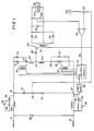
- the inverter includes two series circuits, each having an SCR 18 or 20, and an inductor or choke 42 or 44. Typically, each inductor has a magnitude of 10 microhenries.
- Control circuit 34 alternately triggers the two SCRS through pulse transformers 30, 32, each pulse transformer being connected between the gate and cathode of a respective SCR. The frequency at which the SCRS are fired determines the output voltage, as will become apparent below.
- the resonant output circuit includes a capacitor 46 and a load.
- the actual circuitry depicted for the load in Fig. 1 is one which is often found in practice.
- the inverter functions to transform the DC input potential to an AC potential across a load. In a typical application, however, what is desired is a DC potential.
- Fig. 1 is a standard rectifier which includes a transformer 48, a pair of diodes 50 and a filter capacitor 52, together with a "real" load 56.
- a feedback circuit In order to control the amplitude of the DC output potential, a feedback circuit is employed. Resistors 54a, 54b feed a fraction of the output voltage to the plus input of difference amplifier 60. A reference potential 64 is extended through a variable potentiometer 62 to the minus input of the difference amplifier. The amplifier output is thus an indication of the difference between the actual DC potential derived and that which is desired. The output of the amplifier is extended to the input of control circuit 34.
- the control circuit is simply a voltage-to-frequency converter which alternately pulses transformers 30, 32 at a repetition frequency determined by the potential on control line 36.
- the voltage-to-frequency converter of control circuit 34 provides a polarity reversal so that an increase in voltage on the control line 36 causes a corresponding reduction in frequency.
- capacitors 70, 72 may be twenty times as large in magnitude as capacitor 46 (e.g. capacitor 46 may be only 1 microfarad), so the effect of capacitors 70, 72 on the resulting resonance is small. (This is equivalent to treating the effective DC input potential between terminal 10 and node 24 as constituting a zero-impedance power supply).
- this device Each time that this device is fired, it causes a current to flow in the reverse direction through the capacitor, thus giving rise to an AC potential across the output transformer. Assuming a short-circuited load, however, the current through capacitor 46 and the voltage at node 22 are both zero at the end of a single cycle of resonance through the series circuit which includes SCR 20.
- Fig. 2 depicts several current and voltage waveforms for the case of a short-circuited load.
- the first waveform represents the current through capacitor 46, with positive current being in the left-to-right direction and with the peak currents typically being about 50 amperes and -50 amperes respectively.
- SCR 18 is fired and a resonating current starts to flow through the SCR, inductor 42 and capacitor 46.
- the current reaches a peak of 50 amperes when the supply potential of 150 volts appears at node 22 (the second waveform of Fig. 2).
- the current then starts to decrease and goes to zero at time 3b, with the potential at node 22 rising to. 300 volts and the SCR turning off.
- a negative current flows, and the voltage at node 22 returns to zero.
- time 3c current stops flowing and the voltage at node 22 remains at zero.
- SCR 20 is triggered. Now current first flows from right to left through the capacitor. At time 3e, SCR 20 turns off and the voltage at node 22 is at -300 volts. Diode 40 conducts during the second half-cycle, all current flow ceasing at time 3f.
- the third waveform on Fig. 2 depicts the voltage at node 27.
- SCR 18 or diode 30 conducts and node 27 is held at the 150-volt potential at terminal 10.
- the potential at node 27 simply tracks that at node 22. Similar remarks apply to the fourth waveform of Fig. 2 which depicts the voltage at node 29.
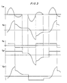
- FIG. 3 depicts four waveforms comparable to those of Fig. 2 for a non-zero load, one which results in a voltage waveform at node 33 (across the primary winding of transformer 48) which alternates between +100 and -100 volts.
- the waveform at node 33 is also shown in Fig. 3.
- one of the main advantages of the prior art type circuit of Fig. 1 is that whenever an SCR is fired, the resulting current constitutes only a single cycle of an oscillatory waveform, the current flowing through the SCR during-the first-half-cycle and through the respective commutating diode during the second half-cycle.
- the SCR turns off automatically when the current drops below the "holding" value, the diode turns off at the end of the cycle when the current attempts to reverse direction once again, and there is no second cycle of conduction because the SCR remains off.
- the rate at which the SCRs are fired determines the total power delivered to the load, and thus a simple voltage-to-frequency control circuit can be employed to vary the output potential across the load.
- the system of Fig. 1 is provided with protection against simultaneous conduction of the SCRs, a condition known as shoot-through and which might otherwise damage the SCRs and result in shut down of the power supply.
- capacitor 46 has a magnitude of one microfarad.
- the peak current which is reached when inductor 42 (or inductor 44) resonates with capacitor 46 is proportional to the square root of the ratio of the capacitance of capacitor 46 to the inductance of inductor 42.
- the peak current which is achieved when capacitors 70, 72 resonate with inductors 42, 44 is proportional to the square root of the ratio of the magnitude of one of the capacitors to the magnitude of one of the inductors.
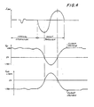
- the two lower waveforms in Fig. 4 depict the voltages at nodes 41 and 43.
- the nominal voltages are +150 and -150 volts respectively, with the voltages changing slightly whenever one of inductors 42 or 44 resonates with capacitor 46 during normal operation. But when a shoot-through occurs, the voltages at nodes 41 and 43 change dramatically as capacitors 70 and 72 resonate with the inductors. Both voltages swing by about 300 volts. At the end of the single-cycle of resonance, the two nodes are clamped and the excessive voltages which would otherwise occur are prevented.
- node 43 rises in potential well above the potential at node 24.
- one-shot multivibrator 80 is triggered.
- the output of the multivibrator is applied to an inhibit input of control circuit 34, the control circuit thus being disabled and no longer applying triggering pulses to the SCRs.
- the period of the multivibrator should be selected in accordance with the particular application. For example, if it is known that when arcing occurs it will be continuous for quite some time, the control circuit should be inhibited for at least this duration. However, in many applications the control circuit needs to be inhibited for a period of perhaps only 200 microseconds to 20 milliseconds. Recovery from the shoot-through fault allows normal inverter operation to resume almost immediately without requiring any manual intervention such as operating a circuit breaker.
- the circuit of Fig. 5 is in many respects similar to that of Fig. 1.
- the main differences relates to the control section, and to the incorporation of four inverter stages ST-1 through ST-4 connected in parallel.
- Gates and drivers 21 trigger respective stages in a manner comparable to that in which the individual stage of Fig. 1 is triggered.
- Terminals 35-2 through 37-4 are connected to respective terminals 29-2 through 31-4 in a manner equivalent to that shown for stage ST-1)
- the circuit 21 simply extends pulses from the voltage-to-frequency converter 19 to a number of pulse transformers 30-1 through 32-4 in accordance with the count of counter 25. For example, if the count is binary 1010, only the pulse transformers associated with stages ST-2 and ST-4 will be pulsed.
- the four resonant circuits are connected in parallel so that the inverter stage currents can be summed together. Because the resonant frequency of a stage is proportional to the product of its inductor (42- or 44-) and capacitor (46-), all stages operate at the same frequency; while the capacitors of successive stages are doubled in magnitude, the inductor magnitudes are halved. At the same time, however, successive stages provide doubled increments of power because the power delivered by any stage is proportional to the square root of its capacitance divided by its inductance. Inverter stage ST-1 provides a maximum of 1/15 of the total power capability of the complete inverter system.
- the basic control circuit comprises a voltage-to-frequency converter 19 which drives the gate electrodes of the SCRs in the four inverter stages ST-1 through ST-4 via logic gates and driver circuits 21. These logic circuits determine which SCRs receive the gate drive pulses generated from the outputs of the voltage-to-frequency converter 19. Control for the logic gates is derived from the input signal to the voltage-to-frequency converter which is an inverse voltage representation of the frequency, and hence the power, of the inverter stages in use at any instant.
- This input voltage is inverted by inverter 61.
- the inverted voltage is applied to voltage comparator 23 which determines a voltage "window" used for triggering up/down counter 25.
- voltage comparator 23 determines a voltage "window" used for triggering up/down counter 25.
- the control voltage at the input of the comparator approaches the high limit trip level determined by voltage source 55 and potentiometer 57.
- the inverter frequency has reached the maximum design limit (e.g. 40 kHz), and a pulse is then sent to the up/down counter to step up the digital counter.
- the outputs from the up/down counter gate on the appropriate combination of SCRs in the inverter stages to produce additional power, in this case equal to that of the lowest power stage.
- the inverter frequency is lowered by the signal from amplifier 60, and the voltage at the input of comparator 23 approaches the low trip level.
- the comparator sends a down control pulse to the up/down counter, reducing the digital counter by unity. This gates the drive to the appropriate combination of inverters so that the available output power is reduced by an amount equal to that of the lowest power stage (least significant bit).
- the output voltage then tends to fall, and the feedback signal causes a control voltage to be applied to the voltage-to-frequency converter 19 so as to increase the frequency and bring the input voltage to the comparator back within the normal operating window.
- the low trip level of comparator 23 should change with the count in the up/down counter since the frequency change with each bit change varies from 2:1 for the lowest bit to 1.07:1 for the highest bit.
- decoder 27 which decodes the output of the up/down counter, and changes the low trip ievel of the comparator so that it tracks the count in the up/down counter.
- the lower frequency limit which is used for any combination of enabled stages is a value which corresponds to a power level less than that which would otherwise be required to restore the frequency back to 40 kHz when the count of counter 25 is decremented.
- the operating frequency will increase to a value less than the upper limit, e.g., 38 kHz.
- the lower frequency limit is reduced in larger and larger increments. The reason for this is that at the lower power levels, the percentage effect of a single bit change on the overall power being delivered at the time is greater.
- This variation in control of the low frequency limit is the function of decoder 27 in Fig. 5.
- the decoder itself is shown in a preferred form in Fig. 6.
- the resistor chain is connected to the minus input of operational amplifier 144, which is provided with a feedback resistor 146 typically equal in value to that of resistor 136.
- the net effect of the arrangement is that the output of the operational amplifier 144, which is a voltage that determines the low frequency limit of comparator 23, varies in accordance with the particular group of stages ST-1 through ST-4 whose operations are enabled.
- Improvements in smoothing the small step in the output voltage during a bit change can be made by decoding the outputs of the up/down counter and applying the decoded output voltage to the input of the voltage-to-frequency converter so as to provide a feed-forward signal while the main control loop takes control.
- Fig. 5 it will be noted that as the feedback signal from the load increases, the output of operational amplifier 60 increases. Because an increasing feedback signal represents a need to reduce the power level, voltage-to-frequency converter 19 operates so that its frequency of operation decreases as its input voltage increases.
- a feed-forward signal circuit is provided which tends to speed up the change in the frequency of operation immediately following a change in the group of stages which are enabled. Operational amplifier 60 is shown on Fig.
- the reason for providing the feed-forward circuit is that following a change in the group of stages whose operations are enabled, it takes some time until the feedback circuit causes a change in the operating frequency. During this transitional period, there may be exhibited a power variation at the output. In order to avoid this, a rapid change in the operating frequency is effected.
- the change is effected by providing an additional operational amplifier 108 (with feedback resistor 109 and isolating resistor 110), together with a resistor chain and associated gates whose operations are controlled by the bit outputs of the up/down counter 25.
- the resistor chain connected to the minus input of operational amplifier 108 is comparable to the resistor chain shown in Fig. 6.
- the resistor magnitudes are selected such that the instantaneous frequency change in each case just cancels out any power level change which might otherwise occur due to the switching of the stages.
- the type of logic, method of control and the number of SCR inverter stages are variables that depend upon the application of the power supply. However, these variables do not affect the basic principles of the invention which requires a multiple number of inverter power stages that are switched in as required by the load to keep the inverter frequency high under all loading conditions, and a fine adjustment of frequency to provide precise control of output power at all power levels.
Landscapes
- Engineering & Computer Science (AREA)
- Power Engineering (AREA)
- Inverter Devices (AREA)
Abstract
Claims (7)
Priority Applications (1)
| Application Number | Priority Date | Filing Date | Title |
|---|---|---|---|
| AT83903659T ATE31852T1 (de) | 1982-11-15 | 1983-10-07 | Energieversorgung mit gleichstromeingangsquelle und gepulsten stromversorgungsstufen. |
Applications Claiming Priority (2)
| Application Number | Priority Date | Filing Date | Title |
|---|---|---|---|
| US06/441,660 US4488214A (en) | 1982-11-15 | 1982-11-15 | High-power, high-frequency inverter system with combined digital and analog control |
| US441660 | 1982-11-15 |
Publications (3)
| Publication Number | Publication Date |
|---|---|
| EP0125278A1 EP0125278A1 (fr) | 1984-11-21 |
| EP0125278A4 EP0125278A4 (fr) | 1985-07-30 |
| EP0125278B1 true EP0125278B1 (fr) | 1988-01-07 |
Family
ID=23753773
Family Applications (1)
| Application Number | Title | Priority Date | Filing Date |
|---|---|---|---|
| EP83903659A Expired EP0125278B1 (fr) | 1982-11-15 | 1983-10-07 | Alimentation ayant une source de courant continu d'entree et des etages d'alimentation a courant pulse |
Country Status (6)
| Country | Link |
|---|---|
| US (1) | US4488214A (fr) |
| EP (1) | EP0125278B1 (fr) |
| JP (1) | JPH0655034B2 (fr) |
| CA (1) | CA1206198A (fr) |
| DE (1) | DE3375262D1 (fr) |
| WO (1) | WO1984002041A1 (fr) |
Families Citing this family (15)
| Publication number | Priority date | Publication date | Assignee | Title |
|---|---|---|---|---|
| US4695933A (en) * | 1985-02-11 | 1987-09-22 | Sundstrand Corporation | Multiphase DC-DC series-resonant converter |
| DE3671343D1 (de) * | 1985-07-26 | 1990-06-21 | Bbc Brown Boveri & Cie | Spannungsumrichter. |
| US4805081A (en) * | 1987-06-29 | 1989-02-14 | Spellman High Voltage Electronics Corp. | Multi-mode control systems for high-frequency resonant inverters |
| US4823250A (en) * | 1987-11-05 | 1989-04-18 | Picker International, Inc. | Electronic control for light weight, portable x-ray system |
| JP2707465B2 (ja) * | 1989-06-29 | 1998-01-28 | スタンレー電気株式会社 | インバータ装置 |
| DE69030847T2 (de) * | 1989-07-31 | 1997-09-18 | Fuji Photo Film Co Ltd | Verfahren zur Verarbeitung von farbphotographischem Silberhalogenidmaterial |
| US5146395A (en) * | 1991-08-09 | 1992-09-08 | Mckie Richard L | Power supply including two tank circuits |
| US5324990A (en) * | 1992-04-03 | 1994-06-28 | Cunningham John C | Voltage inverter power conservation circuit |
| US5414238A (en) * | 1992-10-02 | 1995-05-09 | Martin Marietta Corporation | Resonant power supply for an arcjet thruster |
| US5602897A (en) * | 1995-06-29 | 1997-02-11 | Picker International, Inc. | High-voltage power supply for x-ray tubes |
| US5671132A (en) * | 1996-03-13 | 1997-09-23 | Spellman High Voltage Company | High voltage bipolar CT scanner power supply |
| US6946824B2 (en) * | 2001-09-06 | 2005-09-20 | Intel Corporation | Power delivery system having a plurality of stages and method for setting power delivery system parameters |
| FR2834392A1 (fr) * | 2001-12-28 | 2003-07-04 | St Microelectronics Sa | Oscillateur haute tension ayant un temps de reaction rapide |
| US8360977B2 (en) * | 2007-09-27 | 2013-01-29 | Baxter International Inc. | Continuity circuits for detecting access disconnection |
| US7948222B2 (en) | 2009-02-05 | 2011-05-24 | Advanced Micro Devices, Inc. | Asymmetric topology to boost low load efficiency in multi-phase switch-mode power conversion |
Citations (1)
| Publication number | Priority date | Publication date | Assignee | Title |
|---|---|---|---|---|
| US3823262A (en) * | 1972-10-24 | 1974-07-09 | Coloroptics Inc | Facsimile recorder with compensation of the electrosensitive blank nonlinear applied voltage-burn characteristic |
Family Cites Families (4)
| Publication number | Priority date | Publication date | Assignee | Title |
|---|---|---|---|---|
| DE2221200A1 (de) * | 1972-04-29 | 1973-11-08 | Licentia Gmbh | Astabiler impulsgenerator zur erzeugung bipolarer impulse |
| US3823362A (en) * | 1973-02-02 | 1974-07-09 | Gen Electric | Coordinated master-slave converter system for variable-power tank loads |
| JPS5280427A (en) * | 1975-12-26 | 1977-07-06 | Mitsui Shipbuilding Eng | Method of controlling time division type inverter |
| JPS5840916B2 (ja) * | 1978-11-13 | 1983-09-08 | 日本電信電話株式会社 | 自然転流形dc↓−dcコンバ−タ |
-
1982
- 1982-11-15 US US06/441,660 patent/US4488214A/en not_active Expired - Lifetime
-
1983
- 1983-10-07 DE DE8383903659T patent/DE3375262D1/de not_active Expired
- 1983-10-07 WO PCT/US1983/001577 patent/WO1984002041A1/fr not_active Ceased
- 1983-10-07 EP EP83903659A patent/EP0125278B1/fr not_active Expired
- 1983-10-07 JP JP58503588A patent/JPH0655034B2/ja not_active Expired - Fee Related
- 1983-10-28 CA CA000439987A patent/CA1206198A/fr not_active Expired
Patent Citations (1)
| Publication number | Priority date | Publication date | Assignee | Title |
|---|---|---|---|---|
| US3823262A (en) * | 1972-10-24 | 1974-07-09 | Coloroptics Inc | Facsimile recorder with compensation of the electrosensitive blank nonlinear applied voltage-burn characteristic |
Also Published As
| Publication number | Publication date |
|---|---|
| JPS59502051A (ja) | 1984-12-06 |
| EP0125278A1 (fr) | 1984-11-21 |
| US4488214A (en) | 1984-12-11 |
| EP0125278A4 (fr) | 1985-07-30 |
| JPH0655034B2 (ja) | 1994-07-20 |
| WO1984002041A1 (fr) | 1984-05-24 |
| DE3375262D1 (en) | 1988-02-11 |
| CA1206198A (fr) | 1986-06-17 |
Similar Documents
| Publication | Publication Date | Title |
|---|---|---|
| EP0125278B1 (fr) | Alimentation ayant une source de courant continu d'entree et des etages d'alimentation a courant pulse | |
| US4523269A (en) | Series resonance charge transfer regulation method and apparatus | |
| US5629844A (en) | High voltage power supply having multiple high voltage generators | |
| US4709316A (en) | Single-ended DC-to-DC converter with lossless switching | |
| US4686615A (en) | Power supply circuit | |
| US4493017A (en) | Single drive transformer with regenerative winding for p.w.m. supply having alternately conducting power devices | |
| US5121314A (en) | Bi-mode high voltage resonant power supply and method | |
| JP2583258B2 (ja) | 静電電力変換の方法および装置 | |
| US4967333A (en) | Stabilized power supply with reduced ripple factor | |
| US4805081A (en) | Multi-mode control systems for high-frequency resonant inverters | |
| US4742535A (en) | Inverter type X-ray apparatus | |
| JPH02184267A (ja) | 無損失スナッバ・リセット部品を有する直列共振インバータ | |
| EP0107313A1 (fr) | Source d'énergie résonnante commandée par courant | |
| EP0391617B1 (fr) | Méthode et réseau pour modifier le facteur de puissance d'un circuit de commutation non connecté | |
| US4055791A (en) | Self commutated SCR power supply | |
| CA1163677A (fr) | Methode et dispositif de commande pour module d'alimentation resonant | |
| US4514795A (en) | High-voltage generator, notably for an X-ray tube | |
| CA1318349C (fr) | Convertisseur de courant pour circuit resonnant serie et methode de controle connexe | |
| US4253139A (en) | Power conversion and regulation system | |
| JPH0622551A (ja) | 共振型dc−dcコンバータ | |
| US5680301A (en) | Series/parallel resonant converter | |
| US3881146A (en) | Self-commutating flux-gated inverter | |
| JPH08130871A (ja) | Dc−dcコンバータ | |
| CA1192258A (fr) | Inverseur monophase variable | |
| EP0253432B1 (fr) | Convertisseur d'énergie |
Legal Events
| Date | Code | Title | Description |
|---|---|---|---|
| PUAI | Public reference made under article 153(3) epc to a published international application that has entered the european phase |
Free format text: ORIGINAL CODE: 0009012 |
|
| AK | Designated contracting states |
Designated state(s): AT BE CH DE FR GB LI LU NL SE |
|
| 17P | Request for examination filed |
Effective date: 19841102 |
|
| 17Q | First examination report despatched |
Effective date: 19860512 |
|
| GRAA | (expected) grant |
Free format text: ORIGINAL CODE: 0009210 |
|
| AK | Designated contracting states |
Kind code of ref document: B1 Designated state(s): AT BE CH DE FR GB LI LU NL SE |
|
| PG25 | Lapsed in a contracting state [announced via postgrant information from national office to epo] |
Ref country code: LI Effective date: 19880107 Ref country code: CH Effective date: 19880107 Ref country code: BE Effective date: 19880107 Ref country code: AT Effective date: 19880107 |
|
| REF | Corresponds to: |
Ref document number: 31852 Country of ref document: AT Date of ref document: 19880115 Kind code of ref document: T |
|
| PG25 | Lapsed in a contracting state [announced via postgrant information from national office to epo] |
Ref country code: SE Effective date: 19880131 |
|
| REF | Corresponds to: |
Ref document number: 3375262 Country of ref document: DE Date of ref document: 19880211 |
|
| ET | Fr: translation filed | ||
| REG | Reference to a national code |
Ref country code: CH Ref legal event code: PL |
|
| PG25 | Lapsed in a contracting state [announced via postgrant information from national office to epo] |
Ref country code: LU Free format text: LAPSE BECAUSE OF NON-PAYMENT OF DUE FEES Effective date: 19881031 |
|
| PLBE | No opposition filed within time limit |
Free format text: ORIGINAL CODE: 0009261 |
|
| STAA | Information on the status of an ep patent application or granted ep patent |
Free format text: STATUS: NO OPPOSITION FILED WITHIN TIME LIMIT |
|
| 26N | No opposition filed | ||
| REG | Reference to a national code |
Ref country code: GB Ref legal event code: IF02 |
|
| PGFP | Annual fee paid to national office [announced via postgrant information from national office to epo] |
Ref country code: GB Payment date: 20021002 Year of fee payment: 20 |
|
| PGFP | Annual fee paid to national office [announced via postgrant information from national office to epo] |
Ref country code: FR Payment date: 20021008 Year of fee payment: 20 |
|
| PGFP | Annual fee paid to national office [announced via postgrant information from national office to epo] |
Ref country code: DE Payment date: 20021011 Year of fee payment: 20 |
|
| PGFP | Annual fee paid to national office [announced via postgrant information from national office to epo] |
Ref country code: NL Payment date: 20021031 Year of fee payment: 20 |
|
| PG25 | Lapsed in a contracting state [announced via postgrant information from national office to epo] |
Ref country code: GB Free format text: LAPSE BECAUSE OF EXPIRATION OF PROTECTION Effective date: 20031006 |
|
| PG25 | Lapsed in a contracting state [announced via postgrant information from national office to epo] |
Ref country code: NL Free format text: LAPSE BECAUSE OF EXPIRATION OF PROTECTION Effective date: 20031007 |
|
| REG | Reference to a national code |
Ref country code: GB Ref legal event code: PE20 |
|
| NLV7 | Nl: ceased due to reaching the maximum lifetime of a patent |
Effective date: 20031007 |