EP0125335B1 - Equipement pour l'assemblage de circuits électriques - Google Patents
Equipement pour l'assemblage de circuits électriques Download PDFInfo
- Publication number
- EP0125335B1 EP0125335B1 EP83104835A EP83104835A EP0125335B1 EP 0125335 B1 EP0125335 B1 EP 0125335B1 EP 83104835 A EP83104835 A EP 83104835A EP 83104835 A EP83104835 A EP 83104835A EP 0125335 B1 EP0125335 B1 EP 0125335B1
- Authority
- EP
- European Patent Office
- Prior art keywords
- kit
- blocks
- boards
- electrical
- components
- Prior art date
- Legal status (The legal status is an assumption and is not a legal conclusion. Google has not performed a legal analysis and makes no representation as to the accuracy of the status listed.)
- Expired
Links
Images



Classifications
-
- G—PHYSICS
- G09—EDUCATION; CRYPTOGRAPHY; DISPLAY; ADVERTISING; SEALS
- G09B—EDUCATIONAL OR DEMONSTRATION APPLIANCES; APPLIANCES FOR TEACHING, OR COMMUNICATING WITH, THE BLIND, DEAF OR MUTE; MODELS; PLANETARIA; GLOBES; MAPS; DIAGRAMS
- G09B23/00—Models for scientific, medical, or mathematical purposes, e.g. full-sized devices for demonstration purposes
- G09B23/06—Models for scientific, medical, or mathematical purposes, e.g. full-sized devices for demonstration purposes for physics
- G09B23/18—Models for scientific, medical, or mathematical purposes, e.g. full-sized devices for demonstration purposes for physics for electricity or magnetism
- G09B23/183—Models for scientific, medical, or mathematical purposes, e.g. full-sized devices for demonstration purposes for physics for electricity or magnetism for circuits
- G09B23/185—Models for scientific, medical, or mathematical purposes, e.g. full-sized devices for demonstration purposes for physics for electricity or magnetism for circuits for building block systems
Definitions
- the present invention relates to kits for the assembling of electrical or electronic circuitry, particularly for didactical or instructional purposes, namely at schools or for electronics hobbyists.
- DE-A-19 59 943 which discloses a kit for the assembly of electrical circuitry, particu- larlyfor didactical purposes, including, a selection of electrical or electronics components, the components being mounted on prismatic blocks made of a rigid, electrical insulating material having a bottom, side and top surfaces, metallic sockets installed within the blocks, means for releasably fastening the electrical or electronic components to the blocks thereby establishing electrical connection between terminals of said components and said sockets, and openings formed in the blocks for the insertion of wire plugs thereinto.
- this object is achieved by changing a kit such as known from DE-A-19 59 943 in such a manner that each component is mounted on an insulated board having extensions of a conductive material to which the component's terminals are electrically connected; the boards are adapted to be interchangeably and releasably mounted on the top surface of one of said prismatic blocks, said boards are releasably fastened to the blocks by means of said fastening means in a manner establishing electrical connection between a conductive extension of a board and a socket; and said openings for the insertion of wire plugs thereinto are formed in side surfaces of the block and in each socket.
- the boards are made from a printed-circuit panel whereby the conductive extensions are strips prepared by etching.
- the blocks may have a recessed top surface for receiving the boards, and then said fastening means may be screws received through holes in the boards into tapped bores formed in said sockets.
- the conductive extensions may be in abutting contact with the sockets and/or the holes may be encircled by crimped metal eyelets, the eyelets being in electrical contacts with the conductive extensions and/ or the sockets may be cylindrical, inserted into blind bores formed in the block.
- the components may comprise multiple-terminal components, such as resistors, transistors and integrated circuits; while much as with prior art kit it may include a junction block comprising a single socket with four of said openings.
- the openings in the blocks with a coloured polarity indicating washer.
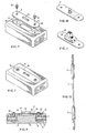
- any circuit built of the kit according to the present invention will be composed of any suitable number of "building-bricks" constituted by the prismatic blocks marked A illustrated in the drawings.
- the blocks A are made of a rigid, electrically insulating material, preferably wood, and being more-or-less of a size of a matchbox for the easy handling thereof even by young students.
- a recess B of a generally rectangular (or other) shape, and a second, smaller recess C, for purposes to be described later.
- blind bores D there are two cylindrical metallic sockets E (see Fig. 5) each having a tapped, axial bore F and a radial, blind bore G.
- Bores G are in alignment with bores H having a sunk shoulder I forming a seat for a coloured, polarity identification plastic washer J fitted into the opposite, short side-walls of the block A.
- a board or small plate K of an electrically insulated material which board is preferably punched-out of standard printed-circuit board or panel and conforms the shape and size of the recess B.
- Board K has two holes L at its sides, (which may be encircled by metallic eyelets denoted L' in Figs. 17-19).
- a pair of conductive strips M are formed (by etching if a printed circuit panel is used) at the bottom side of the board, preferably around the holes L with an extension towards the center of the board.
- a resistor N is mounted on the other, top-side of the board K, with legs P penetrating the board and soldered each to one of the conductive strips M.
- the resistor printed-circuit board K is adapted to be assembled or affixed onto the block A (see Fig. 7), fitting into the cavity or recess B, by a pair of screws Q, as shown in Figs. 8 and 9. Cavity C thus leaves room for the soldered legs P, while the board K is neatly seated within the cavity B.
- plates or boards K carrying various other electrical or electronic components such as a light emitting diode (Fig. 10) or a switch as shown in Fig. 11.
- FIG. 13a and 13b A simple example of use of the invention is illustrated in Figs. 13a and 13b: A power source in the form of a battery U is connected via the switch R to a bulb socket V by the wiring S.
- the resemblance of the physical circuit, built-up of the components according to the present invention, to the schematic diagram of the circuit shown in Figs. 13a is striking. This, together with the most simple handling and assembling procedures required for building the circuit, emphasizes the advantage of the present invention from all aspects.
- Fig. 14 illustrates the assembly of a three-legs component, such as transistor W, on a block A comprising three metallic sockets (not shown) underside a circular board K', electrically connected by the printed circuit strips (not shown) to the legs of the transistor W.
- the blocks A for this purpose will comprise three plug-in washers 3 for the three plugs T of the wires S.
- Fig. 15 shows a similar block A with a central single metallic socket X serving a junction for three or four wires, where connections in parallel are required.
- FIG. 16 there is exemplified in Fig. 16 the mounting of an I.C. (Integrated Circuit) component Y with eight legs to a base block A in a similar manner as with respect to the more simple components.
- I.C. Integrated Circuit
- kit devised according to the present invention paves the way to a great many possibilities, from the most simple wirings to more complicated circuits, using a limited number of the more-expensive blocks A and a larger stock of the less-expensive electronic components each associated with a printed circuit board, such boards being readily exchangeably mountable on the blocks.
- FIGs. 17-19 a modified embodiment of the invention is illustrated employing differently designed metallic socket members E' (Fig. 19) electrically as-well-as mechanically connected to the printed-circuit board K through and by the screws Q'.
- metallic socket members E' Fig. 19
- metal eyelet members L' should be provided, crimped around the holes L in contact with the circular portion of the conductive strips M (see Fig. 6c).
Landscapes
- General Physics & Mathematics (AREA)
- Engineering & Computer Science (AREA)
- Physics & Mathematics (AREA)
- Business, Economics & Management (AREA)
- Mathematical Analysis (AREA)
- Mathematical Optimization (AREA)
- Mathematical Physics (AREA)
- Pure & Applied Mathematics (AREA)
- Computational Mathematics (AREA)
- Algebra (AREA)
- Educational Administration (AREA)
- Educational Technology (AREA)
- Theoretical Computer Science (AREA)
- Coupling Device And Connection With Printed Circuit (AREA)
- Combinations Of Printed Boards (AREA)
- Details Of Connecting Devices For Male And Female Coupling (AREA)
Claims (10)
Priority Applications (3)
| Application Number | Priority Date | Filing Date | Title |
|---|---|---|---|
| DE8383104835T DE3371429D1 (en) | 1983-05-17 | 1983-05-17 | A kit for the assembly of electrical circuits |
| EP83104835A EP0125335B1 (fr) | 1983-05-17 | 1983-05-17 | Equipement pour l'assemblage de circuits électriques |
| AT83104835T ATE27071T1 (de) | 1983-05-17 | 1983-05-17 | Bausatz fuer den aufbau elektrischer schaltkreise. |
Applications Claiming Priority (1)
| Application Number | Priority Date | Filing Date | Title |
|---|---|---|---|
| EP83104835A EP0125335B1 (fr) | 1983-05-17 | 1983-05-17 | Equipement pour l'assemblage de circuits électriques |
Publications (2)
| Publication Number | Publication Date |
|---|---|
| EP0125335A1 EP0125335A1 (fr) | 1984-11-21 |
| EP0125335B1 true EP0125335B1 (fr) | 1987-05-06 |
Family
ID=8190473
Family Applications (1)
| Application Number | Title | Priority Date | Filing Date |
|---|---|---|---|
| EP83104835A Expired EP0125335B1 (fr) | 1983-05-17 | 1983-05-17 | Equipement pour l'assemblage de circuits électriques |
Country Status (3)
| Country | Link |
|---|---|
| EP (1) | EP0125335B1 (fr) |
| AT (1) | ATE27071T1 (fr) |
| DE (1) | DE3371429D1 (fr) |
Cited By (1)
| Publication number | Priority date | Publication date | Assignee | Title |
|---|---|---|---|---|
| US8371894B1 (en) | 2011-12-23 | 2013-02-12 | LaRose Industries, LLC | Illuminated toy construction kit |
Family Cites Families (5)
| Publication number | Priority date | Publication date | Assignee | Title |
|---|---|---|---|---|
| US2878587A (en) * | 1953-06-22 | 1959-03-24 | Arthur R Jubenville | Plug-in mounting block for electrical instruction board |
| US3175304A (en) * | 1961-05-12 | 1965-03-30 | Edward J Och | Educational device for teaching electrical circuit theory, fundamentals, electronics, and the like |
| FR1547183A (fr) * | 1967-12-14 | 1968-11-22 | Ensemble de circuit intégré | |
| FR1562114A (fr) * | 1968-01-31 | 1969-04-04 | ||
| DE1959943A1 (de) * | 1969-11-28 | 1971-06-03 | Siemens Ag | Bausatz zum Aufbau elektrischer Schaltungen |
-
1983
- 1983-05-17 AT AT83104835T patent/ATE27071T1/de not_active IP Right Cessation
- 1983-05-17 EP EP83104835A patent/EP0125335B1/fr not_active Expired
- 1983-05-17 DE DE8383104835T patent/DE3371429D1/de not_active Expired
Cited By (1)
| Publication number | Priority date | Publication date | Assignee | Title |
|---|---|---|---|---|
| US8371894B1 (en) | 2011-12-23 | 2013-02-12 | LaRose Industries, LLC | Illuminated toy construction kit |
Also Published As
| Publication number | Publication date |
|---|---|
| EP0125335A1 (fr) | 1984-11-21 |
| DE3371429D1 (en) | 1987-06-11 |
| ATE27071T1 (de) | 1987-05-15 |
Similar Documents
| Publication | Publication Date | Title |
|---|---|---|
| US12496531B2 (en) | Circuit blocks | |
| US7758349B2 (en) | Magnetic component connector, circuit boards for use therewith, and kits for building and designing circuits | |
| US4449942A (en) | Kit for the assembly of electrical circuits | |
| US5742486A (en) | Reusable electronic circuit building set with interchangeable modular components | |
| DE3377181D1 (en) | Electrical connector for interconnecting printed circuit boards | |
| US7273377B2 (en) | Breadboard to stackable plug convertor | |
| EP0135633B1 (fr) | Eléments de circuits électroniques combinables munis de joints pour une fixation multidirectionelle | |
| US4457721A (en) | Construction kit for electrical circuits | |
| US3745510A (en) | Printed circuit board/integrated circuit socket combination | |
| EP0125335A1 (fr) | Equipement pour l'assemblage de circuits électriques | |
| JPH041666Y2 (fr) | ||
| RU2101773C1 (ru) | Набор элементов для сборки электрических цепей | |
| EP0196636A2 (fr) | Appareil d'enregistrement et de démonstration pour circuits électriques | |
| JPS5853570Y2 (ja) | 電気回路教習具 | |
| KR890009016Y1 (ko) | 통전 단자가 내장된 회로판 | |
| JPH0617333Y2 (ja) | プリント配線板用接続端子 | |
| KR200244024Y1 (ko) | 전자 회로 학습 키트 | |
| GB2301929A (en) | Electronic educational kits | |
| KR880003083Y1 (ko) | 전자회로 교습구의 회로 연결장치 | |
| KR200251939Y1 (ko) | 전자회로 학습키트용 일체형 만능기판 및 인쇄회로기판 | |
| KR200209628Y1 (ko) | 자석칠판을 이용한 전자회로 교육 제작도구 | |
| CZ3484U1 (cs) | Modulová stavebnice k vytváření elektrických a/nebo elektronických obvodů | |
| KR200456723Y1 (ko) | 전자회로 학습용 기판 | |
| JPH01163343U (fr) | ||
| KR19980058787U (ko) | 교육용 회로보드 결합장치 |
Legal Events
| Date | Code | Title | Description |
|---|---|---|---|
| PUAI | Public reference made under article 153(3) epc to a published international application that has entered the european phase |
Free format text: ORIGINAL CODE: 0009012 |
|
| 17P | Request for examination filed |
Effective date: 19830517 |
|
| AK | Designated contracting states |
Designated state(s): AT BE CH DE FR GB IT LI NL SE |
|
| 17Q | First examination report despatched |
Effective date: 19860130 |
|
| ITF | It: translation for a ep patent filed | ||
| GRAA | (expected) grant |
Free format text: ORIGINAL CODE: 0009210 |
|
| AK | Designated contracting states |
Kind code of ref document: B1 Designated state(s): AT BE CH DE FR GB IT LI NL SE |
|
| PG25 | Lapsed in a contracting state [announced via postgrant information from national office to epo] |
Ref country code: BE Effective date: 19870506 Ref country code: AT Effective date: 19870506 |
|
| REF | Corresponds to: |
Ref document number: 27071 Country of ref document: AT Date of ref document: 19870515 Kind code of ref document: T |
|
| REF | Corresponds to: |
Ref document number: 3371429 Country of ref document: DE Date of ref document: 19870611 |
|
| ET | Fr: translation filed | ||
| PLBE | No opposition filed within time limit |
Free format text: ORIGINAL CODE: 0009261 |
|
| STAA | Information on the status of an ep patent application or granted ep patent |
Free format text: STATUS: NO OPPOSITION FILED WITHIN TIME LIMIT |
|
| 26N | No opposition filed | ||
| PGFP | Annual fee paid to national office [announced via postgrant information from national office to epo] |
Ref country code: NL Payment date: 19900531 Year of fee payment: 8 |
|
| ITTA | It: last paid annual fee | ||
| PG25 | Lapsed in a contracting state [announced via postgrant information from national office to epo] |
Ref country code: NL Effective date: 19911201 |
|
| NLV4 | Nl: lapsed or anulled due to non-payment of the annual fee | ||
| PGFP | Annual fee paid to national office [announced via postgrant information from national office to epo] |
Ref country code: SE Payment date: 19940510 Year of fee payment: 12 |
|
| PGFP | Annual fee paid to national office [announced via postgrant information from national office to epo] |
Ref country code: CH Payment date: 19940531 Year of fee payment: 12 |
|
| EAL | Se: european patent in force in sweden |
Ref document number: 83104835.0 |
|
| PG25 | Lapsed in a contracting state [announced via postgrant information from national office to epo] |
Ref country code: SE Effective date: 19950518 |
|
| PG25 | Lapsed in a contracting state [announced via postgrant information from national office to epo] |
Ref country code: LI Effective date: 19950531 Ref country code: CH Effective date: 19950531 |
|
| REG | Reference to a national code |
Ref country code: CH Ref legal event code: PL |
|
| EUG | Se: european patent has lapsed |
Ref document number: 83104835.0 |
|
| PGFP | Annual fee paid to national office [announced via postgrant information from national office to epo] |
Ref country code: DE Payment date: 19980627 Year of fee payment: 16 |
|
| PGFP | Annual fee paid to national office [announced via postgrant information from national office to epo] |
Ref country code: GB Payment date: 19990517 Year of fee payment: 17 |
|
| PG25 | Lapsed in a contracting state [announced via postgrant information from national office to epo] |
Ref country code: DE Free format text: LAPSE BECAUSE OF NON-PAYMENT OF DUE FEES Effective date: 20000301 |
|
| PG25 | Lapsed in a contracting state [announced via postgrant information from national office to epo] |
Ref country code: GB Free format text: LAPSE BECAUSE OF NON-PAYMENT OF DUE FEES Effective date: 20000517 |
|
| PGFP | Annual fee paid to national office [announced via postgrant information from national office to epo] |
Ref country code: FR Payment date: 20000522 Year of fee payment: 18 |
|
| GBPC | Gb: european patent ceased through non-payment of renewal fee |
Effective date: 20000517 |
|
| PG25 | Lapsed in a contracting state [announced via postgrant information from national office to epo] |
Ref country code: FR Free format text: LAPSE BECAUSE OF NON-PAYMENT OF DUE FEES Effective date: 20020131 |