EP0126155B1 - Supports revetus pour enregistrement optique et procede de fabrication - Google Patents
Supports revetus pour enregistrement optique et procede de fabrication Download PDFInfo
- Publication number
- EP0126155B1 EP0126155B1 EP84900208A EP84900208A EP0126155B1 EP 0126155 B1 EP0126155 B1 EP 0126155B1 EP 84900208 A EP84900208 A EP 84900208A EP 84900208 A EP84900208 A EP 84900208A EP 0126155 B1 EP0126155 B1 EP 0126155B1
- Authority
- EP
- European Patent Office
- Prior art keywords
- layer
- absorber
- recording
- optical
- spacer
- Prior art date
- Legal status (The legal status is an assumption and is not a legal conclusion. Google has not performed a legal analysis and makes no representation as to the accuracy of the status listed.)
- Expired
Links
- 230000003287 optical effect Effects 0.000 title claims abstract description 49
- 238000004519 manufacturing process Methods 0.000 title description 7
- 239000006096 absorbing agent Substances 0.000 claims abstract description 85
- 229920002313 fluoropolymer Polymers 0.000 claims abstract description 17
- 239000004811 fluoropolymer Substances 0.000 claims abstract description 14
- 229920000642 polymer Polymers 0.000 claims abstract description 9
- 239000000463 material Substances 0.000 claims description 36
- 239000004812 Fluorinated ethylene propylene Substances 0.000 claims description 33
- 229920009441 perflouroethylene propylene Polymers 0.000 claims description 33
- 229920001343 polytetrafluoroethylene Polymers 0.000 claims description 16
- 239000004810 polytetrafluoroethylene Substances 0.000 claims description 16
- 238000000034 method Methods 0.000 claims description 15
- 238000004132 cross linking Methods 0.000 claims description 7
- 238000007738 vacuum evaporation Methods 0.000 claims description 6
- -1 polytetrafluoroethylene Polymers 0.000 claims description 5
- 230000005855 radiation Effects 0.000 claims description 4
- HQQADJVZYDDRJT-UHFFFAOYSA-N ethene;prop-1-ene Chemical group C=C.CC=C HQQADJVZYDDRJT-UHFFFAOYSA-N 0.000 claims description 3
- 238000009499 grossing Methods 0.000 claims description 3
- 238000005286 illumination Methods 0.000 claims description 3
- 229910000838 Al alloy Inorganic materials 0.000 claims description 2
- 238000001704 evaporation Methods 0.000 claims description 2
- 230000008569 process Effects 0.000 claims description 2
- 238000005137 deposition process Methods 0.000 claims 1
- 125000006850 spacer group Chemical group 0.000 abstract description 50
- 238000002310 reflectometry Methods 0.000 abstract description 10
- 229910052782 aluminium Inorganic materials 0.000 abstract description 9
- XAGFODPZIPBFFR-UHFFFAOYSA-N aluminium Chemical compound [Al] XAGFODPZIPBFFR-UHFFFAOYSA-N 0.000 abstract description 9
- 230000001681 protective effect Effects 0.000 abstract description 6
- NIXOWILDQLNWCW-UHFFFAOYSA-N acrylic acid group Chemical group C(C=C)(=O)O NIXOWILDQLNWCW-UHFFFAOYSA-N 0.000 abstract description 3
- 238000013500 data storage Methods 0.000 abstract description 3
- 239000010410 layer Substances 0.000 description 111
- VYPSYNLAJGMNEJ-UHFFFAOYSA-N Silicium dioxide Chemical compound O=[Si]=O VYPSYNLAJGMNEJ-UHFFFAOYSA-N 0.000 description 35
- 239000010408 film Substances 0.000 description 25
- 230000035945 sensitivity Effects 0.000 description 21
- 238000000576 coating method Methods 0.000 description 20
- 229910052681 coesite Inorganic materials 0.000 description 20
- 229910052906 cristobalite Inorganic materials 0.000 description 20
- 229910052682 stishovite Inorganic materials 0.000 description 20
- 229910052905 tridymite Inorganic materials 0.000 description 20
- 239000000758 substrate Substances 0.000 description 14
- 238000000151 deposition Methods 0.000 description 11
- 239000011248 coating agent Substances 0.000 description 10
- 238000003860 storage Methods 0.000 description 10
- 229910052714 tellurium Inorganic materials 0.000 description 9
- PORWMNRCUJJQNO-UHFFFAOYSA-N tellurium atom Chemical compound [Te] PORWMNRCUJJQNO-UHFFFAOYSA-N 0.000 description 9
- 229910052751 metal Inorganic materials 0.000 description 8
- 239000002184 metal Substances 0.000 description 8
- 230000008021 deposition Effects 0.000 description 7
- 239000000377 silicon dioxide Substances 0.000 description 7
- 239000000428 dust Substances 0.000 description 6
- 230000004888 barrier function Effects 0.000 description 5
- 239000000356 contaminant Substances 0.000 description 5
- 239000002245 particle Substances 0.000 description 5
- 230000006870 function Effects 0.000 description 4
- 239000005350 fused silica glass Substances 0.000 description 4
- 230000008018 melting Effects 0.000 description 4
- 238000002844 melting Methods 0.000 description 4
- 238000006116 polymerization reaction Methods 0.000 description 4
- BFKJFAAPBSQJPD-UHFFFAOYSA-N tetrafluoroethene Chemical group FC(F)=C(F)F BFKJFAAPBSQJPD-UHFFFAOYSA-N 0.000 description 4
- 239000004809 Teflon Substances 0.000 description 3
- 229920006362 Teflon® Polymers 0.000 description 3
- 230000008901 benefit Effects 0.000 description 3
- 230000015556 catabolic process Effects 0.000 description 3
- 230000008859 change Effects 0.000 description 3
- 238000010276 construction Methods 0.000 description 3
- 230000000694 effects Effects 0.000 description 3
- 238000005516 engineering process Methods 0.000 description 3
- 230000007613 environmental effect Effects 0.000 description 3
- 239000011521 glass Substances 0.000 description 3
- 238000010438 heat treatment Methods 0.000 description 3
- 238000002955 isolation Methods 0.000 description 3
- 239000011368 organic material Substances 0.000 description 3
- 239000011241 protective layer Substances 0.000 description 3
- 235000012239 silicon dioxide Nutrition 0.000 description 3
- LIVNPJMFVYWSIS-UHFFFAOYSA-N silicon monoxide Chemical compound [Si-]#[O+] LIVNPJMFVYWSIS-UHFFFAOYSA-N 0.000 description 3
- 229910052814 silicon oxide Inorganic materials 0.000 description 3
- 238000001228 spectrum Methods 0.000 description 3
- 239000000126 substance Substances 0.000 description 3
- 238000012360 testing method Methods 0.000 description 3
- BPQQTUXANYXVAA-UHFFFAOYSA-N Orthosilicate Chemical compound [O-][Si]([O-])([O-])[O-] BPQQTUXANYXVAA-UHFFFAOYSA-N 0.000 description 2
- RTAQQCXQSZGOHL-UHFFFAOYSA-N Titanium Chemical compound [Ti] RTAQQCXQSZGOHL-UHFFFAOYSA-N 0.000 description 2
- 229920006397 acrylic thermoplastic Polymers 0.000 description 2
- 230000004075 alteration Effects 0.000 description 2
- 230000003667 anti-reflective effect Effects 0.000 description 2
- 238000013459 approach Methods 0.000 description 2
- 230000015572 biosynthetic process Effects 0.000 description 2
- 238000006731 degradation reaction Methods 0.000 description 2
- 238000013461 design Methods 0.000 description 2
- 229920001971 elastomer Polymers 0.000 description 2
- 239000000806 elastomer Substances 0.000 description 2
- HCDGVLDPFQMKDK-UHFFFAOYSA-N hexafluoropropylene Chemical group FC(F)=C(F)C(F)(F)F HCDGVLDPFQMKDK-UHFFFAOYSA-N 0.000 description 2
- 230000001965 increasing effect Effects 0.000 description 2
- 238000009413 insulation Methods 0.000 description 2
- 230000002452 interceptive effect Effects 0.000 description 2
- 239000003921 oil Substances 0.000 description 2
- 230000003647 oxidation Effects 0.000 description 2
- 238000007254 oxidation reaction Methods 0.000 description 2
- 229910052760 oxygen Inorganic materials 0.000 description 2
- 229920003229 poly(methyl methacrylate) Polymers 0.000 description 2
- 238000002360 preparation method Methods 0.000 description 2
- 229920005989 resin Chemical class 0.000 description 2
- 239000011347 resin Chemical class 0.000 description 2
- 238000012552 review Methods 0.000 description 2
- 238000007789 sealing Methods 0.000 description 2
- 229920002379 silicone rubber Polymers 0.000 description 2
- 239000011232 storage material Substances 0.000 description 2
- ISXSCDLOGDJUNJ-UHFFFAOYSA-N tert-butyl prop-2-enoate Chemical compound CC(C)(C)OC(=O)C=C ISXSCDLOGDJUNJ-UHFFFAOYSA-N 0.000 description 2
- 239000010409 thin film Substances 0.000 description 2
- 239000010936 titanium Substances 0.000 description 2
- 229910052719 titanium Inorganic materials 0.000 description 2
- XLYOFNOQVPJJNP-UHFFFAOYSA-N water Chemical compound O XLYOFNOQVPJJNP-UHFFFAOYSA-N 0.000 description 2
- 239000004215 Carbon black (E152) Substances 0.000 description 1
- PXGOKWXKJXAPGV-UHFFFAOYSA-N Fluorine Chemical compound FF PXGOKWXKJXAPGV-UHFFFAOYSA-N 0.000 description 1
- 241000197200 Gallinago media Species 0.000 description 1
- UFHFLCQGNIYNRP-UHFFFAOYSA-N Hydrogen Chemical compound [H][H] UFHFLCQGNIYNRP-UHFFFAOYSA-N 0.000 description 1
- 241000243142 Porifera Species 0.000 description 1
- XUIMIQQOPSSXEZ-UHFFFAOYSA-N Silicon Chemical compound [Si] XUIMIQQOPSSXEZ-UHFFFAOYSA-N 0.000 description 1
- 238000005299 abrasion Methods 0.000 description 1
- 239000002253 acid Substances 0.000 description 1
- 150000007513 acids Chemical class 0.000 description 1
- 239000000853 adhesive Substances 0.000 description 1
- 230000001070 adhesive effect Effects 0.000 description 1
- QVGXLLKOCUKJST-UHFFFAOYSA-N atomic oxygen Chemical compound [O] QVGXLLKOCUKJST-UHFFFAOYSA-N 0.000 description 1
- 238000009835 boiling Methods 0.000 description 1
- 239000003054 catalyst Substances 0.000 description 1
- 239000003795 chemical substances by application Substances 0.000 description 1
- 150000008280 chlorinated hydrocarbons Chemical class 0.000 description 1
- 230000001010 compromised effect Effects 0.000 description 1
- 229920001577 copolymer Polymers 0.000 description 1
- 229920006037 cross link polymer Polymers 0.000 description 1
- 238000007766 curtain coating Methods 0.000 description 1
- 230000001351 cycling effect Effects 0.000 description 1
- 230000003247 decreasing effect Effects 0.000 description 1
- 230000000593 degrading effect Effects 0.000 description 1
- 230000032798 delamination Effects 0.000 description 1
- 230000002939 deleterious effect Effects 0.000 description 1
- 239000003989 dielectric material Substances 0.000 description 1
- 238000003618 dip coating Methods 0.000 description 1
- 230000002708 enhancing effect Effects 0.000 description 1
- 230000001747 exhibiting effect Effects 0.000 description 1
- 229910052731 fluorine Inorganic materials 0.000 description 1
- 239000011737 fluorine Substances 0.000 description 1
- 238000009472 formulation Methods 0.000 description 1
- 239000007789 gas Substances 0.000 description 1
- CPBQJMYROZQQJC-UHFFFAOYSA-N helium neon Chemical compound [He].[Ne] CPBQJMYROZQQJC-UHFFFAOYSA-N 0.000 description 1
- 229930195733 hydrocarbon Natural products 0.000 description 1
- 150000002430 hydrocarbons Chemical class 0.000 description 1
- 239000001257 hydrogen Substances 0.000 description 1
- 229910052739 hydrogen Inorganic materials 0.000 description 1
- 230000006872 improvement Effects 0.000 description 1
- 230000001939 inductive effect Effects 0.000 description 1
- 238000002347 injection Methods 0.000 description 1
- 239000007924 injection Substances 0.000 description 1
- 230000007246 mechanism Effects 0.000 description 1
- 238000005272 metallurgy Methods 0.000 description 1
- 150000002739 metals Chemical class 0.000 description 1
- 239000000203 mixture Substances 0.000 description 1
- 239000000178 monomer Substances 0.000 description 1
- 238000013021 overheating Methods 0.000 description 1
- 239000001301 oxygen Substances 0.000 description 1
- 230000035699 permeability Effects 0.000 description 1
- 239000004033 plastic Substances 0.000 description 1
- 229920003023 plastic Polymers 0.000 description 1
- 229920000052 poly(p-xylylene) Polymers 0.000 description 1
- 238000012545 processing Methods 0.000 description 1
- 239000010453 quartz Substances 0.000 description 1
- 150000003254 radicals Chemical class 0.000 description 1
- 230000009257 reactivity Effects 0.000 description 1
- 238000011084 recovery Methods 0.000 description 1
- 230000002829 reductive effect Effects 0.000 description 1
- 229920000260 silastic Polymers 0.000 description 1
- 229910052710 silicon Inorganic materials 0.000 description 1
- 239000010703 silicon Substances 0.000 description 1
- 229920002050 silicone resin Polymers 0.000 description 1
- 239000004945 silicone rubber Substances 0.000 description 1
- 239000002356 single layer Substances 0.000 description 1
- 239000000779 smoke Substances 0.000 description 1
- 239000007779 soft material Substances 0.000 description 1
- 239000007787 solid Substances 0.000 description 1
- 238000004528 spin coating Methods 0.000 description 1
- 235000012461 sponges Nutrition 0.000 description 1
- 238000005507 spraying Methods 0.000 description 1
- 238000004544 sputter deposition Methods 0.000 description 1
- 150000003445 sucroses Chemical class 0.000 description 1
- 230000008961 swelling Effects 0.000 description 1
- 230000007704 transition Effects 0.000 description 1
- 238000013519 translation Methods 0.000 description 1
- 238000009834 vaporization Methods 0.000 description 1
- 230000008016 vaporization Effects 0.000 description 1
- 239000002699 waste material Substances 0.000 description 1
- 238000009736 wetting Methods 0.000 description 1
Images


Classifications
-
- G—PHYSICS
- G11—INFORMATION STORAGE
- G11B—INFORMATION STORAGE BASED ON RELATIVE MOVEMENT BETWEEN RECORD CARRIER AND TRANSDUCER
- G11B7/00—Recording or reproducing by optical means, e.g. recording using a thermal beam of optical radiation by modifying optical properties or the physical structure, reproducing using an optical beam at lower power by sensing optical properties; Record carriers therefor
- G11B7/24—Record carriers characterised by shape, structure or physical properties, or by the selection of the material
- G11B7/241—Record carriers characterised by shape, structure or physical properties, or by the selection of the material characterised by the selection of the material
- G11B7/252—Record carriers characterised by shape, structure or physical properties, or by the selection of the material characterised by the selection of the material of layers other than recording layers
- G11B7/254—Record carriers characterised by shape, structure or physical properties, or by the selection of the material characterised by the selection of the material of layers other than recording layers of protective topcoat layers
- G11B7/2542—Record carriers characterised by shape, structure or physical properties, or by the selection of the material characterised by the selection of the material of layers other than recording layers of protective topcoat layers consisting essentially of organic resins
-
- G—PHYSICS
- G11—INFORMATION STORAGE
- G11B—INFORMATION STORAGE BASED ON RELATIVE MOVEMENT BETWEEN RECORD CARRIER AND TRANSDUCER
- G11B7/00—Recording or reproducing by optical means, e.g. recording using a thermal beam of optical radiation by modifying optical properties or the physical structure, reproducing using an optical beam at lower power by sensing optical properties; Record carriers therefor
- G11B7/24—Record carriers characterised by shape, structure or physical properties, or by the selection of the material
- G11B7/241—Record carriers characterised by shape, structure or physical properties, or by the selection of the material characterised by the selection of the material
- G11B7/242—Record carriers characterised by shape, structure or physical properties, or by the selection of the material characterised by the selection of the material of recording layers
- G11B7/243—Record carriers characterised by shape, structure or physical properties, or by the selection of the material characterised by the selection of the material of recording layers comprising inorganic materials only, e.g. ablative layers
- G11B2007/24302—Metals or metalloids
- G11B2007/24306—Metals or metalloids transition metal elements of groups 3-10
-
- G—PHYSICS
- G11—INFORMATION STORAGE
- G11B—INFORMATION STORAGE BASED ON RELATIVE MOVEMENT BETWEEN RECORD CARRIER AND TRANSDUCER
- G11B7/00—Recording or reproducing by optical means, e.g. recording using a thermal beam of optical radiation by modifying optical properties or the physical structure, reproducing using an optical beam at lower power by sensing optical properties; Record carriers therefor
- G11B7/24—Record carriers characterised by shape, structure or physical properties, or by the selection of the material
- G11B7/241—Record carriers characterised by shape, structure or physical properties, or by the selection of the material characterised by the selection of the material
- G11B7/252—Record carriers characterised by shape, structure or physical properties, or by the selection of the material characterised by the selection of the material of layers other than recording layers
-
- G—PHYSICS
- G11—INFORMATION STORAGE
- G11B—INFORMATION STORAGE BASED ON RELATIVE MOVEMENT BETWEEN RECORD CARRIER AND TRANSDUCER
- G11B7/00—Recording or reproducing by optical means, e.g. recording using a thermal beam of optical radiation by modifying optical properties or the physical structure, reproducing using an optical beam at lower power by sensing optical properties; Record carriers therefor
- G11B7/24—Record carriers characterised by shape, structure or physical properties, or by the selection of the material
- G11B7/241—Record carriers characterised by shape, structure or physical properties, or by the selection of the material characterised by the selection of the material
- G11B7/252—Record carriers characterised by shape, structure or physical properties, or by the selection of the material characterised by the selection of the material of layers other than recording layers
- G11B7/258—Record carriers characterised by shape, structure or physical properties, or by the selection of the material characterised by the selection of the material of layers other than recording layers of reflective layers
- G11B7/2585—Record carriers characterised by shape, structure or physical properties, or by the selection of the material characterised by the selection of the material of layers other than recording layers of reflective layers based on aluminium
Definitions
- the present invention relates to a novel high density information storage medium, and more particularly to such a medium including a recording layer adapted for optical data recording having protective overcoat means and related coatings adapted to enhance recording characteristics.
- Optical storage of digital data is a relatively new technology, concerned with the storage and retrieval of digital information utilizing optical techniques and using a special related (ODD, "optical digital data") medium, such as an ODD disk.
- ODD optical digital data
- ODD optical digital data
- optical data storage technology is attractive because it promises increased storage capacity.
- An optical data disk as here contemplated will be assumed to store information thereon for an extended archival life; the goal is 5-10 years or more under typical, and extreme, service conditions for data processing (DP) apparatus.
- DP data processing
- Such extended life is a goal as yet unattained in the art, though workers have long striven towards it.
- the present invention points toward improved ODD media better adapted for such archival life; media which are especially adapted for "optical mass memory” and like applications, with emphasis on improved overcoat and/or spacer means.
- the spacer layer may preferably comprise a "soft pad” which is vapor-deposited on a reflector layer, and upon which the absorber (recording) layer may in turn be deposited.
- This spacer layer may comprise a so-deposited fluoropolymer which is highly transparent to the contemplated read-write wavelengths and which also provides good thermal and mechanical insulation, isolating the absorber layer from the reflector layer, (note the reflector is typically a highly conductive metal which could otherwise function as a heat sink, draining recording energy away from the absorber layer and reducing its effectiveness).
- a vacuum-evaporated fluoropolymer like polytetrafluoroethylene (PTFE) or fluorinated ethylene propylene copolymer (FEP).
- PTFE polytetrafluoroethylene
- FEP fluorinated ethylene propylene copolymer
- silicate coating silicon oxide or silicon dioxide-cf "fused silica" for such a spacer
- a hard silicate coating for such a spacer
- such material cannot satisfy all the thermal and mechanical objectives here set out.
- silicate coatings conduct heat too readily.
- a "low-energy" recording pulse moderate-to-lows power for about 40 n.sec
- Si0 2 is used (atop AI reflector)-this very thin spacer evidently allows too much recording heat to escape and be wasted.
- bits are contemplated as being about one micrometer in diameter.
- surface "dirt” e.g., oil, fingerprints
- particulate contaminants such as air-borne dust
- bits are this large, or larger, and thus can obstruct a recorded "bit”.
- common smoke particles can be about six microns (6 pm, or about 240 microinches) in diameter. Consequently, such contaminant particles will commonly "mask”, and so obliterate, recorded "bits” (data) if one or several of them sits just above on the overcoat.
- any dust particles that do settle on the surface of such a protective layer, (and are not wiped-away) will be "defocused”; i.e., thrown out of the focal range of the objective used to detect recorded data and the rest of the optical train-optically they "disappear".
- an overcoat should provide mechanical protection for the recording layer and prevent damage from handling, etc. (e.g. during fabrication, testing or service).
- an overcoating which avoids most or all of the foregoing shortcomings, doing so by providing a two-part overcoating made up of a "soft pad” inner layer and a “hard” outer sealing layer-Le. with a “Hard/ Soft” overcoat.
- the soft inner pad is intended to be yielding and quite compressible (as a “mushy cushion") allowing the subjacent absorber to distort and/or move during write-heating, while also providing good thermal insulation (very low thermal conductivity; relatively low specific heat).
- this "soft pad” seems to better isolate the absorber, mechanically and thermally; while the "hard” outer coat gives optimal mechanical protection (e.g. a seal against vapor entry).
- such layers should also bond well, be highly transparent to the contemplated read/write wavelengths and preferably be convenient and inexpensive to apply.
- this "soft pad” overcoat is preferably such as to so decouple the absorber layer (thermally and mechanically) from any supercoating (especially a "hard” layer applied over the "soft pad")- and also to bond favorably with the underlying absorber (e.g. so that sensitivity is not badly compromised and so the absorber is suitably “decoupled” from a hard “outer” overcoating, while also preventing the hard overcoating, and/or any stress therefrom, from constraining the absorber and so interfering with pit-formation therein-yet bonded well enough to the "hard” coat to prevent "delamination", moisture intrusion, etc. in service, these easily upsetting the needed optical properties-cf. a mere 100 A shift can destroy the required "tuning").
- the invention relates to a radiation-recording element comprising a support, a radiation-sensitive absorber layer deformed and/or translated in each bit site during recording, a hard overcoat, and a layer of vacuum deposited fluoropolymer contiguous to the surface of said absorber layer, and located between said absorber layer and said overcoat.
- a radiation-recording element comprising a support, a radiation-sensitive absorber layer deformed and/or translated in each bit site during recording, a hard overcoat, and a layer of vacuum deposited fluoropolymer contiguous to the surface of said absorber layer, and located between said absorber layer and said overcoat.
- the invention is characterised in that said fluoropolymer layer is weakly bonded and obtained by a vacuum evaporation process which modifies evaporating standard fluoropolymer of relatively high molecular weight so that it has a lower molecular weight, less cross-linking and shorter chains.
- Fig. 1 will be understood to (schematically and in idealized fashion) depict a fragmentary section of an optical data disk R-dd, including a substrate disk S supporting a recording tri-layer T and overlying protective overcoat 100.
- Disk R-dd will be understood as intended and adapted for recording by a known radiation source (Laser L) directing a beam LB at tri-layer T so as to record certain bits therein (cf sample "bit-hole” 98-a in absorber layer 98)-these to be "read” using prescribed associated detect means (DET).
- Laser L known radiation source
- DET prescribed associated detect means
- the wavelength of the reading laser beam (LB of Fig. 1) is chosen so that unrecorded regions of disk R-dd exhibit the desired anti-reflection condition; read-beam intensity will be kept low enough so as to not disturb the integrity of data recorded on the disk.
- Substrate S preferably comprises a relatively conventional magnetic recording disk 90 with a smoothing layer 92, applied thereon as necessary.
- Tri-layer T comprises a transparent spacer layer 96 atop a reflector film 94, with a suitable absorber or recording film 98 superposed on layer 96.
- the reflected read-beam will be intensity-modulated by optically detectable changes at bit sites where data was recorded, (e.g., at "hole” 98-a).
- the read beam will experience relatively high reflection when incident on a "bit” (e.g. "hole” 98-a) and relatively low reflection when incident on unwritten regions.
- Protective layer 100 is chosen and arranged so that dust particles on its upper surface will be displaced far from the focal plane of the optical system (i.e. placed out of focus); and so have a negligible effect on the recording and reading operations.
- absorber film 98 at any given bit-site (98-a), must be heated to a prescribed (minimum) write-temperature (Tw).
- Tw write-temperature
- the level of minimum temperature Tw is believed to depend on the properties of absorber 98 (e.g. on its thickness, metallurgy, microscopic structure, etc.) and also on the properties of subjacent spacer 96, as well as upon “interface characteristics" between the spacer 96 and absorber 98, and possibly between overcoat 100 and absorber 98.
- PTFE polytetrafluoroethylene
- FEP fluorinated ethylene propylene copolymer-both are "fluorinated polymers" commercially available (e.g., under the name “Teflon", a trademark of DuPont).
- fluorinated polymers can be vaporized and deposited overthe reflective layer 94 (Fig. 1) in thin uniform layers; especially, for example, by vacuum evaporation from a suitable melt, as discussed below.
- Such coating materials are understood to be in the "vacuum-evaporated/ deposited” state, since they are believed to be in a "modified” state after such deposition.
- the aluminum 94 may be so evaporated under high vacuum, in a large, batch-coating chamber with corresponding large coating distances and "double-rotation" of substrate, etc., to better ensure uniformity. All dust and stains on parts should be reduced to a strict minimum, using rigorous "Clean Room” techniques.
- spacer 96 is similarly deposited atop reflector 94.
- Absorber layer 98 may be understood to comprise a relatively thin layer of tellurium which is vapor-deposited (thermally evaporated) onto spacer layer 96 (on a relatively flat ⁇ 1/ 20 ⁇ record surface thereof).
- Tellurium or some other "absorber metal” having a low melting point and poor conductivity is commonly preferred by workers because it is felt to exhibit superior sensitivity, thus minimizing required (threshold) laser write-power. It is not particularly recommended here because of its poor archivability; but it is very useful for purposes of illustrating the invention because it is so well understood by workers (also because its "deformational" hole-forming mechanism seems well- suited for taking advantage of "soft pad super- coats” as here taught).
- the laser beam is focused on bit site of ]-to 1 micron diameter, (i.e. 5000-10,000 A), with a write-pulse about 40 n.sec long-this also accommodating disk rpm of 1800 and associated galvo-mirrorfocus characteristics].
- the optical data disk is constructed to comprise a polished glass substrate on which is laid an aluminum reflective film about 600 A thick; then, on the aluminum, an FEP (fluoroethylene- propylene) copolymer as a "soft pad" spacer layer approximately 1100 A thick, with a tellurium absorber film approximately 66 A thick laid upon the spacer.
- the reflector, spacer and absorber layers are deposited, in a single continuous sequence and with a single common apparatus, by vacuum evaporation, as described above and consistent with present good practice.
- the material is resistance-wire heated in a "boat" or like vessel in the high-vacuum chamber (e.g., FEP rods may be cut to convenient sizes for placement in the boat; relatively little heat is needed to vaporize the FEP since its boiling point is quite low. Electron gun vaporization is disfa- vored as it will likely decompose FEP). And in certain instances, a like chlorinated hydrocarbon, such as "Parylene” (Union Carbide, Trade Name), may be substituted.
- Parylene Union Carbide, Trade Name
- a "modified" form of FEP will be understood as so-deposited; e.g., when a relatively high molecular wt. fluoropolymer like "Teflon 140" by DuPont is cut from rods into bits and so vacuum evaporated, we conjecture that it deposits, on the AI reflector film as a "different" polymer, probably of lower molecular wt. and characterized by shorter-chains, cross-linked weakly, if at all, (e.g., it is so soft and weakly-bonded, a finger stroke will wipe it off).
- the FEP breaks down, then migrates to the relatively cool AI surface when it condenses and re-polymerizes (whereas when so heated in air, FEP is believed to decompose into perfluoro-propylene and tetrafluoroethylene monomers).
- Fluoropolymers like FEP and PTFE are of a generally paraffinic structure, with some or all of the hydrogen replaced by fluorine. Both are sold by DuPont Co. under the trademark "TEFLON". They are highly inert (unaffected by reactive chemicals) and are quite stable chemically and mechanically, under the contemplated extremes of temperature and humidity; they have low dielectric constants and appear to bond satisfactorily.
- FEP copolymer is made by copolymerizing tetrafluoroethylene and hexafluoropropylene. FEP has a crystalline melting point of 290°C and its molecular structure consists predominantly of linear chains as:
- PTFE is a highly crystalline fully-fluorinated polymer made by (free radical initiated) polymerization of tetrafluoroethylene.
- PTFE polymer has a crystalline melting point of 327°C; its molecular structure consists predominately of linear chains, as:
- an AI substrate should be somewhat reactive and can likely promote polymerization and cross-linking (like a "Ziegler catalyst"; e.g. cf. article by M.S. Toy, 34 J. Polym. Sci. 273,1971), as well as possibly inducing a relatively strong chemical bond either to AI metal or to an AI intermediate.
- a "Ziegler catalyst” e.g. cf. article by M.S. Toy, 34 J. Polym. Sci. 273,1971
- cross-linking of the FEP would be expected to be maximal immediately adjacent the AI film, and to decrease as one proceeded away from the AI up through the FEP-spacer thickness. (This may, or may not, be significant for deriving the desired "absorber isolation", enhanced sensitivity, etc.).
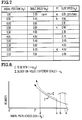
- Sensitivity will be understood as characterizing the write-energy E w , i.e., the laser beam necessary to change reflectivity (or a like read-out characteristic) sufficient to give the specified minimum read-out.
- the intensity and time exposure of the focused Write-Beam here will be understood as sufficient to so elevate the temperature of absorber layer 98 as to cause the indicated change in reflectivity, giving desired read-out quality, etc. (e.g. so that adequate contrast, S/N ratio) may be realized, as understood by workers in the art,-cf an exemplary S/N ratio of 40-50 dB (peak-to-peak signal vs. RMS noise) for a bandwidth of about 15 Mhz.
- FEP gives the desired adhesion, bonding rather strongly to the AI reflector film, but differently (evidently) to the overlying (Te) absorber film.
- This enhanced sensitivity may also be accounted-for, in part, by the mentioned difference in cross-linking through the FEP thickness and by the same disaffinity of the absorber to bond strongly with FEP.
- cross-linking was found to be at a maximum immediately adjacent the Al layer, while decreasing (lower density) as one proceeds away from the AI, and weakest adjacent the Te absorber.
- This difference in cross-linking and in bonding is believed helpful toward reducing heat-leakage from the absorber and also to better accommodate deformation or movement of a bit site when the absorber is written-upon; i.e. this "soft pad” spacer yields nicely, adjacent absorber 98-a during writing and evidently present little or no resistance to the formation of a "hole”-something believed responsible for the enhanced sensitivity this Sample exhibits.
- the FEP gives a nice optically-clear layer with a relatively low refractive index (about 1.3 vs. about 1.5 for fused silica, a value somewhat higher than optimum).
- Sample II-A i.e. Sample O, as so- overcoated
- Sample II-A gave no satisfactory read-out. This is a striking difference in sensitivity-something not fully appreciated heretofore, and evidently due to the improved heat conservation and mechanical compliance of the "soft pad" spacer.
- such a "soft pad” layer might be advantageous as a “buffer” supercoat over an absorber layer, e.g. helping to further isolate it thermally and mechanically-especially where a like "soft pad” was present underneath the absorber. For instance, it was projected that this might further help in conserving write-energy, while giving a "bit hole” more freedom to move or deform while being write-heated (e.g. vs. a silica supercoat which is believed to seriously constrict hole-formation). On both counts sensitivity should be enhanced.
- the disk of Sample II is duplicated, except that the absorber film is covered with a layer of FEP (like the spacer layer, and likewise deposited), about 9500 A thick (no SiO 2 supercoat).
- the disk of Sample III is duplicated, except that the substrate disk is a standard aluminum "Winchester” disk (as used in commercial magnetic recording disks for computer media).
- a "soft pad spacer” may be otherwise implemented in appropriate instances (e.g. with another "soft” relatively non-reactive, stable, durable, imperfectly cured, or weakly polymerized and lightly cross-linked, polymer, such as modified polytetrafluoroethylene, a chloro-fluoro polymer, which will typically decompose and repolymerize in similar fashion or other like modified fluoropol- mers).
- other deposition techniques will, in appropriate cases, be feasible, such as with a plasma deposition technique like glow-discharge (especially for fluoro-carbons) or sputtering, especially where chemical breakdown is not complete.
- Disk R D in Fig. 2 illustrates a preferred example of the features mentioned above, and especially the (general) teaching of a "Hard” overcoat applied over a "soft pad” layer covering an absorber recording film-i.e. a novel "Hard/Soft” overcoating structure O-C (cf Fig. 1, Hard coat g and soft pad layer f over absorber e, which is part of the same sort of ODD "tri-layer" T-L as before, applied on substrate S'). It will now be described with reference to this schematic showing.
- substrate portion may be thought of as the aluminum substrate disk A, treated, when necessary, with a smoothing or subbing layer B to make the surface sufficiently smooth.
- substrate A is preferably a common "Winchester" disk, of an aluminum alloy and prepared as is typical for fabricating disks for high speed magnetic recording of digital data (e.g., as used in computer memory systems).
- the surface of such disks is commonly polished, diamond-turned or otherwise smoothed, as workers well know.
- a suitable glass or plastic disk may be substituted in certain instances.
- “Subbing” layer B will be understood as applied to the bare, well-cleaned disk surface.
- the “subbing” preferbaly comprises an organic material to so smooth the microscopic irregularities on the surface of substrate A to well under "hole size” (e.g., about 0.5 pm or less in diameter). If the surface is already smooth enough (e.g. if a highly polished glass disk is used), a subbing layer may not be necessary, as workers know.
- This substrate is thus understood as preferably comprising a 14" disk to be operated at about 1800 (to several thousand) rpm, with good surface smoothness.
- a radiation (laser) beam of prescribed energy and wavelength will be understood as applied to medium R D from a laser source L (see Fig. 1), being activated and focused at "write time” so as to render a "pit", “hole” or like optical "anomaly” apt for the contemplated read-out on recording layer e in the course of "writing” (e.g. analogous to site 98-a in Fig. 1). More particularly, one may, for example, contemplate using a 10 mW gaussian beam with diameter of 0.8 Il m (i.e. 8000 A) and scanning at 45 m/sec, to form an optical transition with a certain minimum length and width, e.g. 0.8 pm 2 , though not necessarily square, circular or other prescribed shape. Now, this requirement is too stringent for conventional means, as workers realize (e.g. for archival records).
- the coating parameters here will be understood as selected to preferably provide an "anti-reflective" condition for the so-coated disk at the contemplated recording frequency when the write beam is focused on this absorber layer.
- the recording face of disk R D may be visualized as an "absorber layer” (e) together with an appropriate subjacent “spacer layer” (d) and a “reflector layer” (c), below spacer d, as well known in the art.
- aborber layer e
- spacer layer d
- c spacer layer
- c reflector layer
- Such layers (c, d and e) are preferably applied by successive evaporative coating sequences with appropriate materials in a single high-vacuum chamber, and preferably together with "soft pad” overcoating (f) also as described below.
- these applications might be rendered by a suitable plasma polymerization technique or other appropriate methods for producing films of the mentioned type.
- Workers will recognize, as a feature of advantage here, the teaching of materials and techniques which may accommodate such a series of like deposition steps using a common deposition apparatus, (e.g. especially where spacer layer d and a soft overcoating f both comprise like "soft pads").
- Reflector layer c comprises, preferably, a layer of high reflectivity metal such as vapor-deposited aluminum as above discussed, e.g., deposited until layer c is "just opaque” under the contemplated illumination, as viewed through layer c (as workers knowledgable about making evaporated reflectors well know, too thick a reflector will degrade reflectivity). And as workers know, other metals can be used so long as they provide sufficient high reflectance at the contemplated R/ W wavelengths-however, unless great care is taken, a substitute reflector metal may not yield the reactivity and bonding synergism that AI seems to exhibit with FEP (and equivalent spacer material). Another option is to use dielectric films of alternating high and low index and with a quarter-wave reflector.
- Spacer layer d is intended to function, in combination with the reflector layer c and absorber layer e, to reduce the reflectance of the "tri-layer" assembly to zero, or to some other predetermined reflectance value.
- the materials used will preferably be relatively "non-absorbing" and highly transparent to the contemplated R/W wavelengths.
- the subject spacer material preferably comprises FEP, PTFE or a like fluoropolymer-preferably as vapor-deposited, as above described; e.g., in a common vacuum apparatus, along with layers c and e and with layer f, as well.
- Layer e (Fig. 2, still) is the absorbing film in which the working incident "write energy" is to be concentrated.
- the absorber of Sample I will be assumed.
- Soft pad coating f preferably consists of a convenient thickness (e.g., a few thousand A) of FEP or a like polymer (e.g. preferably and conveniently be the same material and deposition method as for spacer layer d). It is preferably formulated and deposited (on absorber e) as the FEP coatings described above, most preferably using laid-down in the same overall deposition sequence; of with tri-layer T-L for convenience.
- Soft pad supercoating f will be sufficiently yielding and compressible to maximize sensitivity, will be relatively non-porous, thermally insulative, with a relatively low specific heat, as well as being highly transparent to the contemplated R/W wavelengths (Ar) as mentioned above. Also, it will bond firmly to a superposed barrier layer, but couple rather loosely to the underlying absorber (e.g. which preferably will be relatively non-reactive with the "pad”)-also a flash inter- coatings can, of course, be used. It should also be chemically stable, compatible (not project contaminants in record R o ) and able to be matched thermally and mechanically to adjacent layers (i.e., to absorber e and hard coat g). Ideally it will also be cost-effective and convenient to apply (e.g., with same deposition methods and equipment as layers c, d, e).
- FEP and PTFE as above-described will be found to meet most, if not all, these stringent requirements (as summarized in Table I above), though other like materials (e.g. like "weakly-polymerized” fluoropolymers) will be suitable in appropriate instances. And, when such "soft pads” sandwich an absorber on both sides, the "thermal-mechanical isolation” thus afforded will be recognized as exceptional.
- the rest of the overcoating O-C on absorber e (i.e. the outer portion) is made up-according to a related feature hereof-of "Hard" overcoating layer g, preferably of the below-specified acrylics. This serves not only to provide outer mechanical protection and the needed defocusing thickness (with pad f), but also serves as a good vapor barrier and anti-static surface.
- Hard overcoat g and related preferred methods for preparing and applying such are detailed below.
- the thickness of layer g will, to some extent, depend on the optical system used (e.g., correcting spherical aberration in the focusing objective may be involved); it has been found that thicknesses on the order of 100-180 micrometers are quite suitable for this embodiment.
- the "soft pad” overcoat generally described above is specified in some Examples elsewhere (e.g. see Samples I, II, etc. as to structure, materials, preparation, use, with certain results and advantageous characteristics indicated).
- a "soft pad” of FEP or PTFE
- fused silica e.g. reducing required write-energy, giving longer; better environmental stability and service-especially in respect of moisture uptake-e.g., when combined with a suitable "Hard” overcoating).
- the "Hard” overcoat resulting will exhibit the usual properties expected of such a protective outercoat (e.g., hardness, abrasion resistance, non-tacky), be readily cleaned (e.g., of dust, oil, fingerprints), be clear and transparent to ⁇ r and exhibit low permeability to contaminants like water vapor, oxygen, etc. Also, it bonds satisfactorily to the "soft pad”.
- a protective outercoat e.g., hardness, abrasion resistance, non-tacky
- be readily cleaned e.g., of dust, oil, fingerprints
- be clear and transparent to ⁇ r and exhibit low permeability to contaminants like water vapor, oxygen, etc. Also, it bonds satisfactorily to the "soft pad”.
- Hard coat material is applied by spin- coating (according to present good practice) or by other suitable techniques known to workers (e.g. in certain instances, spray-coating, dip-coating, flow-coating or curtain coating may be feasible alternatives).
- Radiation-cured acrylic coatings like those detailed below will be understood as apt for most instances.
- the hard overcoat may take the form of a transparent sheet, e.g. or quartz, or a similar glassy material, laminated onto the "soft pad” or vice versa-in some instances the "soft pad” may also serve as the adhesive for the Hard coat.
Landscapes
- Thermal Transfer Or Thermal Recording In General (AREA)
- Manufacturing Optical Record Carriers (AREA)
- Optical Record Carriers And Manufacture Thereof (AREA)
Abstract
Claims (5)
Priority Applications (1)
| Application Number | Priority Date | Filing Date | Title |
|---|---|---|---|
| DE8484900208T DE3380609D1 (en) | 1982-11-30 | 1983-11-29 | Coated media for optical recording and method of fabricating |
Applications Claiming Priority (2)
| Application Number | Priority Date | Filing Date | Title |
|---|---|---|---|
| US445554 | 1982-11-30 | ||
| US06/445,554 US5051978A (en) | 1982-11-30 | 1982-11-30 | Coated media for optical recording |
Related Child Applications (8)
| Application Number | Title | Priority Date | Filing Date |
|---|---|---|---|
| EP86117173A Division-Into EP0226945A3 (en) | 1982-11-30 | 1983-11-29 | Coated media for optical recording, with "soft/hard" overcoat |
| EP86117171A Division-Into EP0226943A3 (en) | 1982-11-30 | 1983-11-29 | Coated media for optical recording, associated acrylic coatings and related application methods |
| EP86117171A Division EP0226943A3 (en) | 1982-11-30 | 1983-11-29 | Coated media for optical recording, associated acrylic coatings and related application methods |
| EP86117174A Division-Into EP0230587A3 (en) | 1982-11-30 | 1983-11-29 | Coated media for optical recording and associated coating techniques |
| EP86117174A Division EP0230587A3 (en) | 1982-11-30 | 1983-11-29 | Coated media for optical recording and associated coating techniques |
| EP87113174A Division EP0265641A3 (en) | 1982-11-30 | 1983-11-29 | Coated media for optical recording |
| EP86117172A Division EP0226944A3 (en) | 1982-11-30 | 1983-11-29 | Coated media for optical recording with acrylic overcoat |
| EP86117172A Division-Into EP0226944A3 (en) | 1982-11-30 | 1983-11-29 | Coated media for optical recording with acrylic overcoat |
Publications (3)
| Publication Number | Publication Date |
|---|---|
| EP0126155A1 EP0126155A1 (fr) | 1984-11-28 |
| EP0126155A4 EP0126155A4 (fr) | 1985-06-06 |
| EP0126155B1 true EP0126155B1 (fr) | 1989-09-20 |
Family
ID=23769374
Family Applications (6)
| Application Number | Title | Priority Date | Filing Date |
|---|---|---|---|
| EP84900208A Expired EP0126155B1 (fr) | 1982-11-30 | 1983-11-29 | Supports revetus pour enregistrement optique et procede de fabrication |
| EP86117171A Withdrawn EP0226943A3 (en) | 1982-11-30 | 1983-11-29 | Coated media for optical recording, associated acrylic coatings and related application methods |
| EP87113174A Withdrawn EP0265641A3 (en) | 1982-11-30 | 1983-11-29 | Coated media for optical recording |
| EP86117174A Withdrawn EP0230587A3 (en) | 1982-11-30 | 1983-11-29 | Coated media for optical recording and associated coating techniques |
| EP86117172A Withdrawn EP0226944A3 (en) | 1982-11-30 | 1983-11-29 | Coated media for optical recording with acrylic overcoat |
| EP86117173A Withdrawn EP0226945A3 (en) | 1982-11-30 | 1983-11-29 | Coated media for optical recording, with "soft/hard" overcoat |
Family Applications After (5)
| Application Number | Title | Priority Date | Filing Date |
|---|---|---|---|
| EP86117171A Withdrawn EP0226943A3 (en) | 1982-11-30 | 1983-11-29 | Coated media for optical recording, associated acrylic coatings and related application methods |
| EP87113174A Withdrawn EP0265641A3 (en) | 1982-11-30 | 1983-11-29 | Coated media for optical recording |
| EP86117174A Withdrawn EP0230587A3 (en) | 1982-11-30 | 1983-11-29 | Coated media for optical recording and associated coating techniques |
| EP86117172A Withdrawn EP0226944A3 (en) | 1982-11-30 | 1983-11-29 | Coated media for optical recording with acrylic overcoat |
| EP86117173A Withdrawn EP0226945A3 (en) | 1982-11-30 | 1983-11-29 | Coated media for optical recording, with "soft/hard" overcoat |
Country Status (5)
| Country | Link |
|---|---|
| US (1) | US5051978A (fr) |
| EP (6) | EP0126155B1 (fr) |
| JP (1) | JPS59502124A (fr) |
| DE (1) | DE3380609D1 (fr) |
| WO (1) | WO1984002220A1 (fr) |
Families Citing this family (22)
| Publication number | Priority date | Publication date | Assignee | Title |
|---|---|---|---|---|
| EP0139478B1 (fr) * | 1983-09-23 | 1989-06-28 | Unisys Corporation | Procédé pour déposer une couche superficielle sur des milieux d'enregistrement optique |
| EP0210637B1 (fr) * | 1985-07-31 | 1991-09-11 | E.I. Du Pont De Nemours And Company | Composition optique de couchage |
| JPS62188037A (ja) * | 1986-02-13 | 1987-08-17 | Central Glass Co Ltd | 光情報記録カ−ド |
| JP2542647B2 (ja) * | 1987-11-23 | 1996-10-09 | 太陽誘電株式会社 | 光情報記録媒体 |
| EP0404951B1 (fr) * | 1988-07-01 | 1996-04-24 | Sony Corporation | Support d'enregistrement optique et procede de production de ce support |
| US5759329A (en) * | 1992-01-06 | 1998-06-02 | Pilot Industries, Inc. | Fluoropolymer composite tube and method of preparation |
| US5916404A (en) * | 1992-01-06 | 1999-06-29 | Pilot Industries, Inc. | Fluoropolymer composite tube and method of preparation |
| JPH085167B2 (ja) * | 1992-01-06 | 1996-01-24 | パイロット インダストリーズ、インコーポレイテッド | フルオロポリマー複合材料製チューブおよびその製造方法 |
| US20030168157A1 (en) * | 1992-01-06 | 2003-09-11 | Kuenzel Kenneth J. | Fluoropolymer composite tube and method of preparation |
| US6517657B1 (en) | 1992-01-06 | 2003-02-11 | Pilot Industries, Inc. | Fluoropolymer composite tube and method of preparation |
| US7247313B2 (en) | 2001-06-27 | 2007-07-24 | Advanced Cardiovascular Systems, Inc. | Polyacrylates coatings for implantable medical devices |
| US7396539B1 (en) | 2002-06-21 | 2008-07-08 | Advanced Cardiovascular Systems, Inc. | Stent coatings with engineered drug release rate |
| US7005137B1 (en) | 2002-06-21 | 2006-02-28 | Advanceed Cardiovascular Systems, Inc. | Coating for implantable medical devices |
| US7217426B1 (en) | 2002-06-21 | 2007-05-15 | Advanced Cardiovascular Systems, Inc. | Coatings containing polycationic peptides for cardiovascular therapy |
| US7491233B1 (en) | 2002-07-19 | 2009-02-17 | Advanced Cardiovascular Systems Inc. | Purified polymers for coatings of implantable medical devices |
| US7169178B1 (en) | 2002-11-12 | 2007-01-30 | Advanced Cardiovascular Systems, Inc. | Stent with drug coating |
| US7563454B1 (en) | 2003-05-01 | 2009-07-21 | Advanced Cardiovascular Systems, Inc. | Coatings for implantable medical devices |
| US8791171B2 (en) | 2003-05-01 | 2014-07-29 | Abbott Cardiovascular Systems Inc. | Biodegradable coatings for implantable medical devices |
| US7244443B2 (en) | 2004-08-31 | 2007-07-17 | Advanced Cardiovascular Systems, Inc. | Polymers of fluorinated monomers and hydrophilic monomers |
| US7251089B2 (en) * | 2005-01-07 | 2007-07-31 | Seagate Technology Llc | Storage medium with overcoat layer for enhanced heating |
| US9028859B2 (en) | 2006-07-07 | 2015-05-12 | Advanced Cardiovascular Systems, Inc. | Phase-separated block copolymer coatings for implantable medical devices |
| WO2019236503A1 (fr) * | 2018-06-03 | 2019-12-12 | Inv. Namesurftec, Llc | Compositions d'enveloppement, procédés, et applications pour substrats à faible frottement et durabilité élevée |
Family Cites Families (19)
| Publication number | Priority date | Publication date | Assignee | Title |
|---|---|---|---|---|
| US3342754A (en) | 1966-02-18 | 1967-09-19 | Union Carbide Corp | Para-xylylene polymers |
| US4069487A (en) * | 1974-12-26 | 1978-01-17 | Canon Kabushiki Kaisha | Recording member and process for recording |
| US4216501A (en) | 1977-03-28 | 1980-08-05 | Rca Corporation | Optical anti-reflective information record |
| US4101907A (en) * | 1977-08-29 | 1978-07-18 | Rca Corporation | Overcoat structure for optical video disc |
| US4300143A (en) * | 1977-08-29 | 1981-11-10 | Rca Corporation | Thin protective overcoat layer for optical video disc |
| US4195312A (en) | 1978-02-24 | 1980-03-25 | Rca Corporation | Recorder and antireflective record blank having an optically passive transparent layer |
| US4195313A (en) | 1978-02-24 | 1980-03-25 | Rca Corporation | Antireflective information record having an optically passive transparent layer |
| DE2824403C2 (de) | 1978-06-03 | 1983-07-14 | Veba-Glas Ag, 4300 Essen | Verfahren zum Beschichten von Gegenständen, insbesondere Glasflaschen |
| JPS5558832A (en) | 1978-10-24 | 1980-05-01 | Mitsubishi Electric Corp | Signal recording and reproducing unit of optical type |
| US4222071A (en) | 1978-12-22 | 1980-09-09 | Rca Corporation | Sensitivity information record |
| US4264986A (en) * | 1979-03-12 | 1981-04-28 | Willis Craig I | Information-recording process & apparatus |
| JPS5613534A (en) | 1979-07-16 | 1981-02-09 | Toshiba Corp | Optical recording body and its manufacture |
| US4410581A (en) * | 1979-10-01 | 1983-10-18 | Omex | Laser recording medium |
| US4300227A (en) * | 1979-10-17 | 1981-11-10 | Rca Corporation | Replicable optical recording medium |
| US4340959A (en) | 1979-12-28 | 1982-07-20 | Rca Corporation | Optical recording medium with a thick overcoat |
| JPS6023037B2 (ja) * | 1980-03-18 | 1985-06-05 | 旭化成株式会社 | 情報記録部材 |
| US4340655A (en) * | 1980-06-18 | 1982-07-20 | Eastman Kodak Company | Thermal and mechanical barrier layers for optical recording elements |
| US4363844A (en) * | 1980-09-22 | 1982-12-14 | Lewis Terry W | Metallized information carrying discs |
| US4335173A (en) * | 1980-09-22 | 1982-06-15 | Eastman Kodak Company | Method and means for reducing undesirable effects of dirt particles on a flexible record device |
-
1982
- 1982-11-30 US US06/445,554 patent/US5051978A/en not_active Expired - Lifetime
-
1983
- 1983-11-29 EP EP84900208A patent/EP0126155B1/fr not_active Expired
- 1983-11-29 EP EP86117171A patent/EP0226943A3/en not_active Withdrawn
- 1983-11-29 EP EP87113174A patent/EP0265641A3/en not_active Withdrawn
- 1983-11-29 EP EP86117174A patent/EP0230587A3/en not_active Withdrawn
- 1983-11-29 DE DE8484900208T patent/DE3380609D1/de not_active Expired
- 1983-11-29 JP JP84500197A patent/JPS59502124A/ja active Pending
- 1983-11-29 WO PCT/US1983/001868 patent/WO1984002220A1/fr not_active Ceased
- 1983-11-29 EP EP86117172A patent/EP0226944A3/en not_active Withdrawn
- 1983-11-29 EP EP86117173A patent/EP0226945A3/en not_active Withdrawn
Also Published As
| Publication number | Publication date |
|---|---|
| EP0226945A3 (en) | 1989-04-05 |
| EP0226944A3 (en) | 1989-04-12 |
| US5051978A (en) | 1991-09-24 |
| EP0265641A3 (en) | 1989-04-05 |
| EP0126155A4 (fr) | 1985-06-06 |
| DE3380609D1 (en) | 1989-10-26 |
| WO1984002220A1 (fr) | 1984-06-07 |
| EP0230587A3 (en) | 1989-04-05 |
| EP0226944A2 (fr) | 1987-07-01 |
| EP0226943A2 (fr) | 1987-07-01 |
| EP0126155A1 (fr) | 1984-11-28 |
| EP0230587A2 (fr) | 1987-08-05 |
| EP0226945A2 (fr) | 1987-07-01 |
| EP0265641A2 (fr) | 1988-05-04 |
| EP0226943A3 (en) | 1989-04-05 |
| JPS59502124A (ja) | 1984-12-20 |
Similar Documents
| Publication | Publication Date | Title |
|---|---|---|
| US4981743A (en) | Overcoat composition for optical record | |
| US4492718A (en) | Rotation coating of disk substrate with acrylate prepolymer | |
| US4584259A (en) | Coated media for optical recording with acrylic overcoat | |
| US5051978A (en) | Coated media for optical recording | |
| US6576320B2 (en) | Optical information medium and evaluation method | |
| EP0092113B1 (fr) | Elément d'enregistrement optique pour un système de mémoire optique et un procédé de fabrication de l'élément | |
| US4592939A (en) | Method of rendering uniform coating on disks and product | |
| US4995028A (en) | Coated media for optical recording, with soft/hard overcoat | |
| US4522846A (en) | Spiral-coated media for optical recording | |
| US5171606A (en) | Method of coating an optical media | |
| US5008129A (en) | Methods of fabricating optical records with overcoating | |
| US4539572A (en) | Optical recording medium | |
| EP0139478A1 (fr) | Procédé pour déposer une couche superficielle sur des milieux d'enregistrement optique | |
| CA1267379A (fr) | Surcouche pour support d'enregistrement | |
| WO1984002289A1 (fr) | Supports recouverts pour enregistrements optiques et techniques de revetement relatives | |
| US5177732A (en) | Optical recording using an agglomerating recording medium which changes reflectivity upon recording | |
| CA1277282C (fr) | Methode de deposition d'une surcouche a la surface d'un support d'enregistrement optique | |
| EP0079229A2 (fr) | Dispositif d'emmagasinage de données numériques sur un moyen d'enregistrement optique d'archives à l'aide de rayonnement à faible énergie | |
| JP2000215513A (ja) | 光記録媒体及び光記録装置 | |
| EP0079230A2 (fr) | Préparation de moyens d'enregistrement d'archives pour l'emmagasinage de données numériques | |
| EP0079233A2 (fr) | Procédé d'enregistrement de données d'archives et moyens y associés | |
| EP0079741A2 (fr) | Moyens d'enregistrement d'archives à couche d'informations améliorée et substrat y associé |
Legal Events
| Date | Code | Title | Description |
|---|---|---|---|
| PUAI | Public reference made under article 153(3) epc to a published international application that has entered the european phase |
Free format text: ORIGINAL CODE: 0009012 |
|
| AK | Designated contracting states |
Designated state(s): BE DE FR GB NL SE |
|
| 17P | Request for examination filed |
Effective date: 19841119 |
|
| 17Q | First examination report despatched |
Effective date: 19860801 |
|
| RAP1 | Party data changed (applicant data changed or rights of an application transferred) |
Owner name: BURROUGHS CORPORATION (A DELAWARE CORPORATION) |
|
| D17Q | First examination report despatched (deleted) | ||
| RAP1 | Party data changed (applicant data changed or rights of an application transferred) |
Owner name: UNISYS CORPORATION |
|
| GRAA | (expected) grant |
Free format text: ORIGINAL CODE: 0009210 |
|
| AK | Designated contracting states |
Kind code of ref document: B1 Designated state(s): BE DE FR GB NL SE |
|
| REF | Corresponds to: |
Ref document number: 3380609 Country of ref document: DE Date of ref document: 19891026 |
|
| ET | Fr: translation filed | ||
| PLBE | No opposition filed within time limit |
Free format text: ORIGINAL CODE: 0009261 |
|
| STAA | Information on the status of an ep patent application or granted ep patent |
Free format text: STATUS: NO OPPOSITION FILED WITHIN TIME LIMIT |
|
| 26N | No opposition filed | ||
| PGFP | Annual fee paid to national office [announced via postgrant information from national office to epo] |
Ref country code: FR Payment date: 19910416 Year of fee payment: 9 |
|
| PG25 | Lapsed in a contracting state [announced via postgrant information from national office to epo] |
Ref country code: FR Effective date: 19910731 |
|
| PGFP | Annual fee paid to national office [announced via postgrant information from national office to epo] |
Ref country code: SE Payment date: 19921016 Year of fee payment: 10 |
|
| PGFP | Annual fee paid to national office [announced via postgrant information from national office to epo] |
Ref country code: NL Payment date: 19921130 Year of fee payment: 10 |
|
| PG25 | Lapsed in a contracting state [announced via postgrant information from national office to epo] |
Ref country code: SE Effective date: 19931130 |
|
| PGFP | Annual fee paid to national office [announced via postgrant information from national office to epo] |
Ref country code: BE Payment date: 19931210 Year of fee payment: 11 |
|
| PG25 | Lapsed in a contracting state [announced via postgrant information from national office to epo] |
Ref country code: NL Effective date: 19940601 |
|
| NLV4 | Nl: lapsed or anulled due to non-payment of the annual fee | ||
| PG25 | Lapsed in a contracting state [announced via postgrant information from national office to epo] |
Ref country code: BE Effective date: 19941130 |
|
| EUG | Se: european patent has lapsed |
Ref document number: 84900208.4 Effective date: 19940610 |
|
| BERE | Be: lapsed |
Owner name: UNISYS CORP. Effective date: 19941130 |
|
| PGFP | Annual fee paid to national office [announced via postgrant information from national office to epo] |
Ref country code: GB Payment date: 20001004 Year of fee payment: 18 |
|
| PGFP | Annual fee paid to national office [announced via postgrant information from national office to epo] |
Ref country code: DE Payment date: 20001124 Year of fee payment: 18 |
|
| PG25 | Lapsed in a contracting state [announced via postgrant information from national office to epo] |
Ref country code: GB Free format text: LAPSE BECAUSE OF NON-PAYMENT OF DUE FEES Effective date: 20011129 |
|
| REG | Reference to a national code |
Ref country code: GB Ref legal event code: IF02 |
|
| PG25 | Lapsed in a contracting state [announced via postgrant information from national office to epo] |
Ref country code: DE Free format text: LAPSE BECAUSE OF NON-PAYMENT OF DUE FEES Effective date: 20020702 |
|
| GBPC | Gb: european patent ceased through non-payment of renewal fee |
Effective date: 20011129 |