EP0126384A2 - Procédé et dispositif pour le décodage d'un train de données codé selon le code nB/(n+1)B - Google Patents
Procédé et dispositif pour le décodage d'un train de données codé selon le code nB/(n+1)B Download PDFInfo
- Publication number
- EP0126384A2 EP0126384A2 EP84105259A EP84105259A EP0126384A2 EP 0126384 A2 EP0126384 A2 EP 0126384A2 EP 84105259 A EP84105259 A EP 84105259A EP 84105259 A EP84105259 A EP 84105259A EP 0126384 A2 EP0126384 A2 EP 0126384A2
- Authority
- EP
- European Patent Office
- Prior art keywords
- bit
- clock
- parallel
- data stream
- bits
- Prior art date
- Legal status (The legal status is an assumption and is not a legal conclusion. Google has not performed a legal analysis and makes no representation as to the accuracy of the status listed.)
- Granted
Links
Images

Classifications
-
- H—ELECTRICITY
- H04—ELECTRIC COMMUNICATION TECHNIQUE
- H04L—TRANSMISSION OF DIGITAL INFORMATION, e.g. TELEGRAPHIC COMMUNICATION
- H04L7/00—Arrangements for synchronising receiver with transmitter
- H04L7/0054—Detection of the synchronisation error by features other than the received signal transition
- H04L7/0066—Detection of the synchronisation error by features other than the received signal transition detection of error based on transmission code rule
-
- H—ELECTRICITY
- H04—ELECTRIC COMMUNICATION TECHNIQUE
- H04L—TRANSMISSION OF DIGITAL INFORMATION, e.g. TELEGRAPHIC COMMUNICATION
- H04L25/00—Baseband systems
- H04L25/38—Synchronous or start-stop systems, e.g. for Baudot code
- H04L25/40—Transmitting circuits; Receiving circuits
- H04L25/49—Transmitting circuits; Receiving circuits using code conversion at the transmitter; using predistortion; using insertion of idle bits for obtaining a desired frequency spectrum; using three or more amplitude levels ; Baseband coding techniques specific to data transmission systems
- H04L25/4906—Transmitting circuits; Receiving circuits using code conversion at the transmitter; using predistortion; using insertion of idle bits for obtaining a desired frequency spectrum; using three or more amplitude levels ; Baseband coding techniques specific to data transmission systems using binary codes
- H04L25/4908—Transmitting circuits; Receiving circuits using code conversion at the transmitter; using predistortion; using insertion of idle bits for obtaining a desired frequency spectrum; using three or more amplitude levels ; Baseband coding techniques specific to data transmission systems using binary codes using mBnB codes
Definitions
- the invention relates to a method and an associated arrangement for decoding an nB / (n + 1) B-coded data stream, which consists of words or groups of bits, each with n signal bits and an inserted coding bit.
- nB / (n + 1) B- described for example in the article by R. 0. Carter, n Low-Disparity Binary Coding System "in Electronics Letters, May 1965, Vol. 1, No. 3, pages 67 and 68.
- coding is often used in telecommunications to generate a line code from a simple binary code, the frequency spectrum of which has no DC component and as little as possible at low frequencies, but has as high a portion as possible at half the bit rate, which is as independent as possible of the respective one
- n non-inverted or after n inverted signal bits of the original binary code there follows another - (n + 1) test bit as coding bit, which, for example with the logical value 1 or, 0, indicates that a or no inversion of the original n signal bits on the transmission side or on the transmission link was carried out in order to obtain an equal number of 0 and 1 bits as possible over time in the data stream thus formed to reach.
- the decoding of the nB (n + 1) B code on the receiving side is carried out in a known manner in such a way that a frame structure is required in the original code, which can be recognized in a synchronization circuit of the receiver and with the help of which the exact temporal storage of the n Signal bits and the coding bit is determined by means of logic. Depending on the logical value of the coding bit, the logic then outputs the n associated signal bits either inverted or uninfluenced as the output signal.
- a data stream ⁇ 2 is then available at the output of the receiver, which consists of a continuous series of n signal bits and the bits that characterize the frame structure.
- This conventional method of decoding has the disadvantage that the possible uses are limited by the frame structure of the original code and may vary depending on the frame structure or frame length. can result in very long synchronization times.
- a further disadvantage is that the transmission speed of the useful information is reduced by the insertion of the bits characterizing the frame structure or the transmission speed of the data stream 0 1 over the transmission path must be increased accordingly. This disadvantage also occurs if the frame structure is only identified after the transcoding of the original code into the nB / (n + 1) B code.
- the invention is therefore based on the object of specifying a method which can decode an nB (n + 1) B code even in the absence of bits characterizing the frame structure and furthermore has a comparatively very short synchronization time.
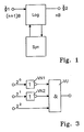
- the exemplary embodiment shown in FIG. 2 is based on a 7B / 8B code as the nB / (n + 1) B code.
- a coding bit belongs to every 7 bits of the original binary code, so that 8 bits each form a bit group.
- Fig. 2 shows a preferred embodiment of an arrangement according to the invention for decoding a 7B / 8B-coded serial data stream 01, which consists of 8-bit groups of bits and has no bits characterizing the frame structure.
- the data stream ⁇ 1 is read into a series / parallel converter SPW with a read clock T 1 and output as a sequence of 8-bit parallel bit groups ⁇ 11 to ⁇ 18 in parallel with a clock speed of 1/8 T 1, the first bit of each Parallel bit groups ⁇ 11 to ⁇ 18 is the coding bit ⁇ 11 and the remaining bits form a parallel signal bit group ⁇ 12 to ⁇ 18.
- the parallel signal bit groups ⁇ 12 to ⁇ 18 are inverted in an inverter I with an associated coding bit ⁇ 11 carrying the logical value 1 or not inverted with a logical value 0.
- the parallel signal bit groups ⁇ 12 + to ⁇ 18 + arrive at an evaluator B, which determines the number of bits with the logical value 1 within each parallel signal bit group and forwards this value as a binary number to the first input of a comparator V.
- a subsequent AND gate U is activated, so that a coding bit 0 11, which is present at the AND gate U and indicates an inversion, can be switched through with the logical value 1 and as an error pulse to the input of a Frequency divider FT with the sub-ratio m: 1 arrives.
- the frequency divider FT emits a pulse to a clock suppression circuit TA, which suppresses a clock pulse from the input clock T 1 of the series / parallel converter SFW.
- This blanking shifts the 8-bit groups contained in the data stream ⁇ 1 by one bit each within the series / parallel converter SPW.
- the order of the signal bits and the coding bit is only cyclically interchanged, so that one of the signal bits controls the Invester.
- the frequency divider FT is set to zero at certain intervals by means of an erase clock T3 which is present at the reset input R.
- the clock frequency of this - preferably coming from a free-running oscillator - delete clock T3 must be greater than the product of the read clock T1 times the error probability divided by the division factor m of the frequency divider FT.
- FIG. 3 shows a further embodiment of the comparator V in FIG. 2.
- no comparison number is entered here and compared with the output signal of the evaluator B in an integrated module with a relatively high signal delay.
- a chip-carrier design of the decoder circuit according to FIG. 2 in ECL technology which has been practically implemented has been successfully tested for bit rates up to 560 Mbit / s.
Landscapes
- Engineering & Computer Science (AREA)
- Computer Networks & Wireless Communication (AREA)
- Signal Processing (AREA)
- Physics & Mathematics (AREA)
- Spectroscopy & Molecular Physics (AREA)
- Compression, Expansion, Code Conversion, And Decoders (AREA)
- Error Detection And Correction (AREA)
- Detection And Prevention Of Errors In Transmission (AREA)
- Reduction Or Emphasis Of Bandwidth Of Signals (AREA)
- Dc Digital Transmission (AREA)
Priority Applications (1)
| Application Number | Priority Date | Filing Date | Title |
|---|---|---|---|
| AT84105259T ATE38112T1 (de) | 1983-05-13 | 1984-05-09 | Verfahren und anordnung zur decodierung eines n.b/(n+1)b-codierten datenstroms. |
Applications Claiming Priority (2)
| Application Number | Priority Date | Filing Date | Title |
|---|---|---|---|
| DE3317466 | 1983-05-13 | ||
| DE19833317466 DE3317466A1 (de) | 1983-05-13 | 1983-05-13 | Verfahren und anordnung zur decodierung eines nb/(n+1) b-codierten datenstroms |
Publications (3)
| Publication Number | Publication Date |
|---|---|
| EP0126384A2 true EP0126384A2 (fr) | 1984-11-28 |
| EP0126384A3 EP0126384A3 (en) | 1986-04-16 |
| EP0126384B1 EP0126384B1 (fr) | 1988-10-19 |
Family
ID=6198912
Family Applications (1)
| Application Number | Title | Priority Date | Filing Date |
|---|---|---|---|
| EP84105259A Expired EP0126384B1 (fr) | 1983-05-13 | 1984-05-09 | Procédé et dispositif pour le décodage d'un train de données codé selon le code nB/(n+1)B |
Country Status (4)
| Country | Link |
|---|---|
| EP (1) | EP0126384B1 (fr) |
| JP (1) | JPS60100832A (fr) |
| AT (1) | ATE38112T1 (fr) |
| DE (2) | DE3317466A1 (fr) |
Cited By (4)
| Publication number | Priority date | Publication date | Assignee | Title |
|---|---|---|---|---|
| WO1991015926A1 (fr) * | 1990-04-10 | 1991-10-17 | British Telecommunications Public Limited Company | Alignement de donnees |
| WO1994016507A1 (fr) * | 1993-01-14 | 1994-07-21 | Apple Computer, Inc. | Separateur de lignes de retard pour bus de donnees |
| EP1170914A3 (fr) * | 2000-07-07 | 2004-10-06 | Infineon Technologies AG | Procédé et dispositif de codage numérique de données binaires avec un spectre de transmission particulier |
| CN116318499A (zh) * | 2022-12-02 | 2023-06-23 | 利尔达科技集团股份有限公司 | 一种基于5g精准授时的智能终端系统及精准授时方法 |
Family Cites Families (3)
| Publication number | Priority date | Publication date | Assignee | Title |
|---|---|---|---|---|
| US3185963A (en) * | 1960-11-25 | 1965-05-25 | Stelma Inc | Synchronizing system having reversible counter means |
| US3241067A (en) * | 1961-04-21 | 1966-03-15 | Bell Telephone Labor Inc | Synchronization of decoder systems based on message wave statistics |
| JPS57162850A (en) * | 1981-03-31 | 1982-10-06 | Fujitsu Ltd | Code error detecting system |
-
1983
- 1983-05-13 DE DE19833317466 patent/DE3317466A1/de not_active Withdrawn
-
1984
- 1984-05-09 EP EP84105259A patent/EP0126384B1/fr not_active Expired
- 1984-05-09 AT AT84105259T patent/ATE38112T1/de not_active IP Right Cessation
- 1984-05-09 DE DE8484105259T patent/DE3474748D1/de not_active Expired
- 1984-05-10 JP JP59091984A patent/JPS60100832A/ja active Granted
Cited By (6)
| Publication number | Priority date | Publication date | Assignee | Title |
|---|---|---|---|---|
| WO1991015926A1 (fr) * | 1990-04-10 | 1991-10-17 | British Telecommunications Public Limited Company | Alignement de donnees |
| WO1994016507A1 (fr) * | 1993-01-14 | 1994-07-21 | Apple Computer, Inc. | Separateur de lignes de retard pour bus de donnees |
| US5412697A (en) * | 1993-01-14 | 1995-05-02 | Apple Computer, Inc. | Delay line separator for data bus |
| US5619541A (en) * | 1993-01-14 | 1997-04-08 | Apple Computer, Inc. | Delay line separator for data bus |
| EP1170914A3 (fr) * | 2000-07-07 | 2004-10-06 | Infineon Technologies AG | Procédé et dispositif de codage numérique de données binaires avec un spectre de transmission particulier |
| CN116318499A (zh) * | 2022-12-02 | 2023-06-23 | 利尔达科技集团股份有限公司 | 一种基于5g精准授时的智能终端系统及精准授时方法 |
Also Published As
| Publication number | Publication date |
|---|---|
| ATE38112T1 (de) | 1988-11-15 |
| DE3317466A1 (de) | 1984-11-15 |
| EP0126384A3 (en) | 1986-04-16 |
| EP0126384B1 (fr) | 1988-10-19 |
| JPS60100832A (ja) | 1985-06-04 |
| DE3474748D1 (en) | 1988-11-24 |
| JPS6366085B2 (fr) | 1988-12-19 |
Similar Documents
| Publication | Publication Date | Title |
|---|---|---|
| DE68923207T2 (de) | Schaltung zur Verhinderung eines metastabilen Zustandes. | |
| DE2121115C2 (de) | Prüfeinrichtung für nichtlineare Schaltkreise | |
| DE69432587T2 (de) | Verzögerungsleitungsseparator für datenbus | |
| DE3779820T2 (de) | Digitale phasenregelschleifen. | |
| EP0078903A1 (fr) | Procédé et arrangement pour assurer la synchronisation initiale d'un télégramme composé de séries d'impulsions d'éléments binaires à l'intérieur d'un récepteur | |
| DE2726277A1 (de) | Abtastsignaldetektor | |
| DE2320422A1 (de) | Verfahren zur fehlererkennung | |
| DE3780406T2 (de) | Verfahren und anordnung zur kodierung und dekodierung binaerer information. | |
| DE19820435B4 (de) | Signalsende- und Empfangsvorrichtung für das Leiterbahnsystem in einem Bauteil mit mehreren Logikwerten | |
| EP0325318B1 (fr) | Central de commutation | |
| DE3442613C2 (fr) | ||
| DE3786041T2 (de) | Kommunikations-Bitmustererkennungsschaltung. | |
| DE2629403A1 (de) | Vorrichtung zur zeitverzoegerung eines analogen informationseingangssignales | |
| DE3786449T2 (de) | Verfahren und Gerät zur Erkennung vorübergehender Fehler. | |
| DE2842371A1 (de) | Verfahren zur synchronisierung von sende- und empfangseinrichtungen | |
| EP0126384A2 (fr) | Procédé et dispositif pour le décodage d'un train de données codé selon le code nB/(n+1)B | |
| DE68919211T2 (de) | Empfänger für seriellen Daten. | |
| DE1934869B2 (de) | Verfahren uns schaltungsanordnung zur kodierung asynchroner binaerer digitalsignale | |
| EP1221220A2 (fr) | Procede et dispositif pour la communication bidirectionnelle entre au moins deux interlocuteurs | |
| EP0591231B1 (fr) | Procede de determination de l'origine d'erreurs sur les bits | |
| DE2326658A1 (de) | Datentrennvorrichtung | |
| DE69120364T2 (de) | Verfahren und Gerät zur Wahrnehmung einer Rahmenbitfolge in einem digitalen Datenübertragungssystem | |
| EP1126615A1 (fr) | Méthode de division de fréquence d'un signal d'horloge et circuit diviseur de fréquence pour réaliser cette méthode | |
| DE69221816T2 (de) | Anordnung und Verfahren zum Zählen von Taktschlupfen | |
| DE3801220A1 (de) | Vielstufiger binaerzaehler mit einer ausstattung zur durchfuehrung von testlaeufen |
Legal Events
| Date | Code | Title | Description |
|---|---|---|---|
| PUAI | Public reference made under article 153(3) epc to a published international application that has entered the european phase |
Free format text: ORIGINAL CODE: 0009012 |
|
| AK | Designated contracting states |
Designated state(s): AT BE CH DE FR GB IT LI NL SE |
|
| PUAL | Search report despatched |
Free format text: ORIGINAL CODE: 0009013 |
|
| AK | Designated contracting states |
Kind code of ref document: A3 Designated state(s): AT BE CH DE FR GB IT LI NL SE |
|
| 17P | Request for examination filed |
Effective date: 19860923 |
|
| 17Q | First examination report despatched |
Effective date: 19880322 |
|
| GRAA | (expected) grant |
Free format text: ORIGINAL CODE: 0009210 |
|
| AK | Designated contracting states |
Kind code of ref document: B1 Designated state(s): AT BE CH DE FR GB IT LI NL SE |
|
| PG25 | Lapsed in a contracting state [announced via postgrant information from national office to epo] |
Ref country code: SE Effective date: 19881019 |
|
| REF | Corresponds to: |
Ref document number: 38112 Country of ref document: AT Date of ref document: 19881115 Kind code of ref document: T |
|
| GBT | Gb: translation of ep patent filed (gb section 77(6)(a)/1977) | ||
| REF | Corresponds to: |
Ref document number: 3474748 Country of ref document: DE Date of ref document: 19881124 |
|
| ET | Fr: translation filed | ||
| ITF | It: translation for a ep patent filed | ||
| PG25 | Lapsed in a contracting state [announced via postgrant information from national office to epo] |
Ref country code: GB Effective date: 19890509 Ref country code: AT Effective date: 19890509 |
|
| PG25 | Lapsed in a contracting state [announced via postgrant information from national office to epo] |
Ref country code: BE Effective date: 19890531 |
|
| PGFP | Annual fee paid to national office [announced via postgrant information from national office to epo] |
Ref country code: DE Payment date: 19890726 Year of fee payment: 6 |
|
| PLBE | No opposition filed within time limit |
Free format text: ORIGINAL CODE: 0009261 |
|
| STAA | Information on the status of an ep patent application or granted ep patent |
Free format text: STATUS: NO OPPOSITION FILED WITHIN TIME LIMIT |
|
| PGFP | Annual fee paid to national office [announced via postgrant information from national office to epo] |
Ref country code: CH Payment date: 19890824 Year of fee payment: 6 |
|
| 26N | No opposition filed | ||
| PG25 | Lapsed in a contracting state [announced via postgrant information from national office to epo] |
Ref country code: NL Effective date: 19891201 |
|
| GBPC | Gb: european patent ceased through non-payment of renewal fee | ||
| NLV4 | Nl: lapsed or anulled due to non-payment of the annual fee | ||
| PG25 | Lapsed in a contracting state [announced via postgrant information from national office to epo] |
Ref country code: FR Free format text: LAPSE BECAUSE OF NON-PAYMENT OF DUE FEES Effective date: 19900131 |
|
| REG | Reference to a national code |
Ref country code: FR Ref legal event code: ST |
|
| PG25 | Lapsed in a contracting state [announced via postgrant information from national office to epo] |
Ref country code: LI Effective date: 19900531 Ref country code: CH Effective date: 19900531 |
|
| REG | Reference to a national code |
Ref country code: CH Ref legal event code: PL |
|
| PG25 | Lapsed in a contracting state [announced via postgrant information from national office to epo] |
Ref country code: DE Effective date: 19910201 |