EP0126803A2 - Procédé pour la conversion photochimique de monoxyde en dioxyde de silicium - Google Patents
Procédé pour la conversion photochimique de monoxyde en dioxyde de silicium Download PDFInfo
- Publication number
- EP0126803A2 EP0126803A2 EP83111643A EP83111643A EP0126803A2 EP 0126803 A2 EP0126803 A2 EP 0126803A2 EP 83111643 A EP83111643 A EP 83111643A EP 83111643 A EP83111643 A EP 83111643A EP 0126803 A2 EP0126803 A2 EP 0126803A2
- Authority
- EP
- European Patent Office
- Prior art keywords
- sio
- layer
- radiation
- oxygen
- converted
- Prior art date
- Legal status (The legal status is an assumption and is not a legal conclusion. Google has not performed a legal analysis and makes no representation as to the accuracy of the status listed.)
- Withdrawn
Links
Images


Classifications
-
- H—ELECTRICITY
- H10—SEMICONDUCTOR DEVICES; ELECTRIC SOLID-STATE DEVICES NOT OTHERWISE PROVIDED FOR
- H10P—GENERIC PROCESSES OR APPARATUS FOR THE MANUFACTURE OR TREATMENT OF DEVICES COVERED BY CLASS H10
- H10P14/00—Formation of materials, e.g. in the shape of layers or pillars
- H10P14/60—Formation of materials, e.g. in the shape of layers or pillars of insulating materials
- H10P14/69—Inorganic materials
- H10P14/692—Inorganic materials composed of oxides, glassy oxides or oxide-based glasses
- H10P14/6921—Inorganic materials composed of oxides, glassy oxides or oxide-based glasses containing silicon
- H10P14/69215—Inorganic materials composed of oxides, glassy oxides or oxide-based glasses containing silicon the material being a silicon oxide, e.g. SiO2
-
- B—PERFORMING OPERATIONS; TRANSPORTING
- B01—PHYSICAL OR CHEMICAL PROCESSES OR APPARATUS IN GENERAL
- B01J—CHEMICAL OR PHYSICAL PROCESSES, e.g. CATALYSIS OR COLLOID CHEMISTRY; THEIR RELEVANT APPARATUS
- B01J19/00—Chemical, physical or physico-chemical processes in general; Their relevant apparatus
- B01J19/08—Processes employing the direct application of electric or wave energy, or particle radiation; Apparatus therefor
- B01J19/12—Processes employing the direct application of electric or wave energy, or particle radiation; Apparatus therefor employing electromagnetic waves
- B01J19/122—Incoherent waves
- B01J19/123—Ultraviolet light
-
- C—CHEMISTRY; METALLURGY
- C01—INORGANIC CHEMISTRY
- C01B—NON-METALLIC ELEMENTS; COMPOUNDS THEREOF; METALLOIDS OR COMPOUNDS THEREOF NOT COVERED BY SUBCLASS C01C
- C01B33/00—Silicon; Compounds thereof
- C01B33/113—Silicon oxides; Hydrates thereof
- C01B33/12—Silica; Hydrates thereof, e.g. lepidoic silicic acid
- C01B33/126—Preparation of silica of undetermined type
-
- C—CHEMISTRY; METALLURGY
- C04—CEMENTS; CONCRETE; ARTIFICIAL STONE; CERAMICS; REFRACTORIES
- C04B—LIME, MAGNESIA; SLAG; CEMENTS; COMPOSITIONS THEREOF, e.g. MORTARS, CONCRETE OR LIKE BUILDING MATERIALS; ARTIFICIAL STONE; CERAMICS; REFRACTORIES; TREATMENT OF NATURAL STONE
- C04B41/00—After-treatment of mortars, concrete, artificial stone or ceramics; Treatment of natural stone
- C04B41/009—After-treatment of mortars, concrete, artificial stone or ceramics; Treatment of natural stone characterised by the material treated
-
- C—CHEMISTRY; METALLURGY
- C04—CEMENTS; CONCRETE; ARTIFICIAL STONE; CERAMICS; REFRACTORIES
- C04B—LIME, MAGNESIA; SLAG; CEMENTS; COMPOSITIONS THEREOF, e.g. MORTARS, CONCRETE OR LIKE BUILDING MATERIALS; ARTIFICIAL STONE; CERAMICS; REFRACTORIES; TREATMENT OF NATURAL STONE
- C04B41/00—After-treatment of mortars, concrete, artificial stone or ceramics; Treatment of natural stone
- C04B41/45—Coating or impregnating, e.g. injection in masonry, partial coating of green or fired ceramics, organic coating compositions for adhering together two concrete elements
- C04B41/50—Coating or impregnating, e.g. injection in masonry, partial coating of green or fired ceramics, organic coating compositions for adhering together two concrete elements with inorganic materials
- C04B41/5025—Coating or impregnating, e.g. injection in masonry, partial coating of green or fired ceramics, organic coating compositions for adhering together two concrete elements with inorganic materials with ceramic materials
- C04B41/5035—Silica
-
- C—CHEMISTRY; METALLURGY
- C04—CEMENTS; CONCRETE; ARTIFICIAL STONE; CERAMICS; REFRACTORIES
- C04B—LIME, MAGNESIA; SLAG; CEMENTS; COMPOSITIONS THEREOF, e.g. MORTARS, CONCRETE OR LIKE BUILDING MATERIALS; ARTIFICIAL STONE; CERAMICS; REFRACTORIES; TREATMENT OF NATURAL STONE
- C04B41/00—After-treatment of mortars, concrete, artificial stone or ceramics; Treatment of natural stone
- C04B41/80—After-treatment of mortars, concrete, artificial stone or ceramics; Treatment of natural stone of only ceramics
- C04B41/81—Coating or impregnation
- C04B41/85—Coating or impregnation with inorganic materials
- C04B41/87—Ceramics
-
- H—ELECTRICITY
- H10—SEMICONDUCTOR DEVICES; ELECTRIC SOLID-STATE DEVICES NOT OTHERWISE PROVIDED FOR
- H10P—GENERIC PROCESSES OR APPARATUS FOR THE MANUFACTURE OR TREATMENT OF DEVICES COVERED BY CLASS H10
- H10P14/00—Formation of materials, e.g. in the shape of layers or pillars
- H10P14/60—Formation of materials, e.g. in the shape of layers or pillars of insulating materials
- H10P14/65—Formation of materials, e.g. in the shape of layers or pillars of insulating materials characterised by treatments performed before or after the formation of the materials
- H10P14/6516—Formation of materials, e.g. in the shape of layers or pillars of insulating materials characterised by treatments performed before or after the formation of the materials of treatments performed after formation of the materials
- H10P14/6518—Formation of materials, e.g. in the shape of layers or pillars of insulating materials characterised by treatments performed before or after the formation of the materials of treatments performed after formation of the materials by introduction of substances into an already-existing insulating layer
- H10P14/6519—Formation of materials, e.g. in the shape of layers or pillars of insulating materials characterised by treatments performed before or after the formation of the materials of treatments performed after formation of the materials by introduction of substances into an already-existing insulating layer the substance being oxygen
-
- H—ELECTRICITY
- H10—SEMICONDUCTOR DEVICES; ELECTRIC SOLID-STATE DEVICES NOT OTHERWISE PROVIDED FOR
- H10P—GENERIC PROCESSES OR APPARATUS FOR THE MANUFACTURE OR TREATMENT OF DEVICES COVERED BY CLASS H10
- H10P14/00—Formation of materials, e.g. in the shape of layers or pillars
- H10P14/60—Formation of materials, e.g. in the shape of layers or pillars of insulating materials
- H10P14/65—Formation of materials, e.g. in the shape of layers or pillars of insulating materials characterised by treatments performed before or after the formation of the materials
- H10P14/6516—Formation of materials, e.g. in the shape of layers or pillars of insulating materials characterised by treatments performed before or after the formation of the materials of treatments performed after formation of the materials
- H10P14/6529—Formation of materials, e.g. in the shape of layers or pillars of insulating materials characterised by treatments performed before or after the formation of the materials of treatments performed after formation of the materials by exposure to a gas or vapour
-
- H—ELECTRICITY
- H10—SEMICONDUCTOR DEVICES; ELECTRIC SOLID-STATE DEVICES NOT OTHERWISE PROVIDED FOR
- H10P—GENERIC PROCESSES OR APPARATUS FOR THE MANUFACTURE OR TREATMENT OF DEVICES COVERED BY CLASS H10
- H10P14/00—Formation of materials, e.g. in the shape of layers or pillars
- H10P14/60—Formation of materials, e.g. in the shape of layers or pillars of insulating materials
- H10P14/65—Formation of materials, e.g. in the shape of layers or pillars of insulating materials characterised by treatments performed before or after the formation of the materials
- H10P14/6516—Formation of materials, e.g. in the shape of layers or pillars of insulating materials characterised by treatments performed before or after the formation of the materials of treatments performed after formation of the materials
- H10P14/6536—Formation of materials, e.g. in the shape of layers or pillars of insulating materials characterised by treatments performed before or after the formation of the materials of treatments performed after formation of the materials by exposure to radiation, e.g. visible light
- H10P14/6538—Formation of materials, e.g. in the shape of layers or pillars of insulating materials characterised by treatments performed before or after the formation of the materials of treatments performed after formation of the materials by exposure to radiation, e.g. visible light by exposure to UV light
Definitions
- This invention relates to a method for photochemically converting SiO to SiO 2 in an atmosphere containing oxygen. Also disclosed is an apparatus for carrying out the method, the apparatus including a vacuum chamber into which the oxygen containing atmosphere can be introduced.
- Oxide insulators are used in many applications, including microelectronic devices and packaging.
- SiO and SiO 2 are widely used in technology such as semiconductor device technology and Josephson device technology. While both SiO and Si0 2 are good insulators, SiO 2 is generally preferred because of its inherent stability and good electrical properties.
- Si0 2 is less porous than SiO, and has a lower dielectric constant than SiO. In thin film circuitry where very thin layers are used, the importance of a low dielectric constant becomes even more critical in order to reduce capacitance.
- SiO and SiO 2 also differ in their abilities to be personalized by etching, and in the techniques in which they are formed. Generally, SiO etches slower than Si0 2 when HF is used, and can be formed at a lower temperature. In particular, good films of SiO 2 cannot be produced at temperatures less than 400°C. This constraint is even more evident when the film has to have a thickness less than 500 nm. However, most technologies would prefer to use fabrication processes wherein the temperatures required for the different steps of the process are as low as possible. In particular, processes used to make Josephson tunnel devices require temperatures which do not exceed approximately 100°C. In such processes, the superconductive materials are adversely affected if the temperatures used during device and circuit fabrication exceed approximately 100°C.
- SiO insulating films are often used, because they can be deposited at temperatures less than about 100 o C .
- SiO is not a preferable material because of its relatively high dielectric constant as compared with that of SiO 2 , and because SiO is not as easily personalized as SiO 2 .
- Layers of SiO of very high quality having stochiometric ratios of 1:1, Si:O can be produced using ultra high vacuums (such as vacuums of 10 -6 Pa in an evaporation system).
- ultra high vacuums such as vacuums of 10 -6 Pa in an evaporation system.
- Such SiO is quite stable and will show very little change to SiO 2 over a period of several years.
- thermal oxidation of SiO to SiO 2 will proceed rapidly. This is a well known approach for converting SiO to SiO 2 , but is disadvantageous due to the high processing temperatures that are required.
- the invention as claimed is intended to meet the above objectives and to remedy the drawbacks hitherto encountered.
- the proposed method is characterized in that it comprises the step of irradiating the SiO that is to be converted to SiO 2 with ultraviolet radiation having wavelengths of less than 220 nm.
- the advantages offered by the invention are mainly that it provides a technique for forming Si0 2 layers of varying thickness and high quality at low temperatures.
- this invention describes a method for converting a first oxide species, into a second oxide species by irradiation of the first oxide species with ultraviolet light of wavelengths less than 220 nm, in an environment including oxygen. More specifically, the invention describes a technique and apparatus for converting SiO to Si0 2 by irradiating SiO with ultraviolet radiation of wavelengths less than 220 nm in an environment including oxygen.
- the irradiation can be either pulsed radiation or continuous wave radiation, and can be provided by either a lamp or a laser.
- the energy fluence in the radiation can be very low, although it is desirable to have sufficient energy fluence to cause a significant photochemical effect to occur.
- energy fluences of at least about 5 mJ/cm 2 /pulse will provide effective conversion to SiO 2 .
- the effect which occurs is a photochemical effect in which SiO absorbs light and is photochemically oxidized with oxygen to produce Si0 2 .
- the environment has to include oxygen for this conversion, and can be air, pure oxygen, or a mixture of gases including oxygen. Water saturated air, steam, etc. are also suitable in the practice of this invention.
- any depth of S iO can be converted to SiO 2 .
- a surface layer of SiO will be converted to Si0 2 but, since SiO 2 is transparent to wavelengths less than 200 nm, the effect of further irradiation will not be hindered. In this way, any depth of SiO can be converted to Si0 2 . Examples will be given showing the total conversion of SiO to Si0 2 for several depths, such as depths of 500 nm or greater.
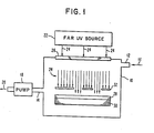
- Fig. 1 shows an apparatus which is suitable for carrying out the present invention.
- the apparatus includes a vacuum chamber 10 having an input port 12 and an output port 14. Gases such as air, water vapor, steam, oxygen, etc. can be introduced into chamber 10 as indicated by arrow 16. The excess gases and volatile byproducts of the reaction can be removed from chamber 10 by using pump 18. The volatile products which are removed are indicated by the arrow 20.
- a far UV source 22 is used to produce radiation 24 having wavelengths less than 220 nm. Radiation 24 passes through window 26 and enters chamber 10. Window 26 is typically comprised of a suprasil quartz window, which will block radiation of wavelengths longer than about 220 nm.
- the source 22 of ultraviolet radiation of this wavelength range can be one which produces either pulsed or continuous wave radiation.
- Two suitable examples are ArF excimer lasers producing a pulsed radiation output at 193 nm and a low pressure mercury resonance lamp producing a continuous wave output at 185 nm.
- the energy fluence available from this laser is greater than that available from the mercury continuous wave source, and can be used to more quickly convert SiO to Si0 2 .
- a suitable ArF laser is one produced by Lambda Physik having Model No. EMG 500.
- the low pressure mercury resonance lamps are also commercially available.
- any type of source or optical system can be used to produce radiation in the wavelength range less than 220 nm for the purposes of this invention.
- the higher power laser sources are generally more efficient in terms of the time involved to produce the necessary photochemical reaction.
- oxide layer 28 is a layer of SiO
- substrate 30 is any material, including metal, semiconductors, insulators, etc.
- radiation 24 is passed through a mask 32 in order to provide irradiation of selected areas of the SiO film 28.
- a blanket irradiation of the entire area of film 28 can also be used. Whether selective area irradiation or blanket irradiation is to be used will depend upon the application of this technique to different processes.
- the effect is a surface effect in which molecules of SiO on the surface are photochemically changed to SiO 2 .
- Si0 2 is transparent to wavelengths in this range, and the process of conversion can continue through the depth of film 28.
- the depth of conversion of SiO to SiO 2 depends upon the length of time the radiation is applied. Any depth of layer 28 can be converted, including its entire thickness.
- the pulsed laser sources generally provide greater energy fluences and therefore are more efficient in terms of the time required to convert SiO to SiO 2 .
- the low pressure mercury lamp can be used effectively for blanket conversion of a thin surface layer of the film 28, in many processes.
- the advantage of a laser providing focused pulse radiation is that smaller areas can be illuminated with good localized control and rapid conversion, especially when a significant depth of SiO has to be converted to SiO 2 .
- FIGS. 2.1 and 2.2 are infrared transmission plots of a sample of SiO, a first portion of which was irradiated with ultraviolet light of wavelengths less than 220 nm in the presence of oxygen, while a second portion thereof was not irradiated.
- FIG. 2.1 is a plot of the portion which was not irradiated
- FIG. 2.2 is a plot of a portion of the sample which was irradiated.
- the sample is a layer of SiO on Si, where the thickness of the SiO layer was 275 nm.
- the irradiation was with laser pulses at 193 nm from an ArF excimer laser. 200 pulses (each of approximate pulse width 10 nsec) were applied.
- the infrared transmission spectrum was examined from 2.5 ⁇ m to 40 ⁇ m. As noted from a comparison of FIGS. 2.1 and 2.2, there is a shift in the transmission of the valley 34, corresponding to the oxidation of the irradiated SiO sample to produce SiO 2 . No peak was seen which would correspond to the presence of Si in the irradiated sample. Thus, there was not merely a rearrangement of atoms within the irradiated sample of the type which would leave free Si and SiO 2 (or SiO). Instead, two molecules of SiO combined with one molecule of oxygen to produce two molecules of SiO 2 .
- SiO and 0 2 could absorb radiation at about 200 nm to produce excited states. Depending upon the lifetime of the excited states, ample time exists for the diffusion of oxygen to provide SiO 2 .
- FIG. 3 is a plot made in a He backscattering experiment.
- 100 nm of SiO was irradiated in air by ultraviolet radiation produced by an ArF laser (193 nm).
- 20,000 pulses were used in the irradiation, each of which had a pulse duration of approximately 10 nsec.
- the energy fluence was about the same as that used in the experiment depicted by FIGS. 2.1 and 2.2 (120 mJ/cm 2 /pulse).
- FIG. 3 the number of counts of backscattered He is plotted against the energy of the backscattered He+.
- He ions are directed to a sample of SiO (solid curve), and are reflected by the sample: After the sample has been irradiated with ultraviolet radiation in accordance with the present invention He ions are again directed to the sample and the dashed curve is obtained.
- the UV irradiation was done in air using 193 nm radiation pulses from an ArF laser.
- the SiO and SiO 2 samples were at a -70 0 tilt with respect to the incoming He ions.
- the ions had an input energy of 2.3 MeV and a charge of 80 ⁇ C.
- the backscattering curve for the layer of SiO (prior to UV irradiation) is given by the solid line.
- the relative composition Si:O of this 100 nm layer of SiO was 49.7:50.3.
- the substrate was Si, on which the SiO layer was deposited or grown.
- the substrate can be any material. The same photochemical effect will occur and SiO will be photochemically converted to SiO 2 .
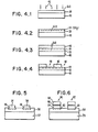
- FIGS. 4.1-4.4 illustrate cre use of this technique to provide a so-called "etch-stop". Such a stop is used to prevent etching of an underlying layer in order to provide removal or patterning of an overlying layer.
- FIG. 4.1 shows a layer 38 of SiO on a substrate 40.
- Layer 38 is given a blanket irradiation by ultraviolet light of wavelengths less than 220 nm, as indicated by the arrows 42. This radiation is applied for only a small amount of time to convert a surface layer 44 of layer 38 to SiO 2 (FIG. 4.2).
- Another layer 46 of SiO is then deposited over converted Si0 2 layer (FIG. 4.3). It is desired to pattern layer 46 by reactive ion etching (RIE). SiO can be etched by CF 4 gas plasmas in reactive ion etching. However, the RIE conditions can be set such that Si0 2 will be etched more slowly than SiO. Thus, the Si0 2 layer 44 will serve as an etch-stop when layer 46 is patterned. This is indicated in FIG. 4.4 where portions 48 of layer 46 have been removed by RIE which stops at the etch-stop provided by Si0 2 layer 44.
- RIE reactive ion etching
- etch-stops are dependent upon differential etch rates which exist for different materials. In the fabrication of devices requiring multilevel thin film technology, etch-stops are very useful. However, such stops are usually provided by depositing layers of different composition, which is an additional process constraint requiring different evaporant sources, etc. In the practice of the present invention, multiple layers of the same composition can be deposited and then converted to a different composition.
- layer 50 is a layer of SiO located on a substrate 52.
- Conductors 54 are to be deposited over SiO layer 50.
- ultraviolet irradiation in an oxygen environment is used to convert regions 56 to Si0 2 . Since the dielectric constant of Si0 2 is significantly less than that of SiO, the signal carrying capabilities of the structure of FIG. 5 will be enhanced.
- regions 56 that are converted to Si0 2 are shown as surface regions in FIG. 5, it is understood that these regions can extend throughout the entire depth of layer 50.
- layer 50 can be made quite thick but then be converted to SiO 2 in order to reduce the dielectric constant beneath the conductors 54. Thicker insulation layers may be required for certain purposes and, since the dielectric constant can be tailored in different locations, the effect of the additional thickness will not be disadvantageous.
- FIG. 6 presents another embodiment that is particularly useful in the fabrication of Josephson effect devices and circuits.
- a layer 58 of SiO is located over the substrate 70.
- Substrate 70 could be an insulator or a superconducting groundplane. Regions 60 of SiO layer 58 have been converted to Si0 2 .
- Josephson effect devices 62 are formed directly over converted layer 60.
- Devices 62 typically comprise the base superconducting electrode 64, a thin tunnel barrier 66, and a top, or counter- superelectrode 68.
- FIG. 6 provides a technique and structure for obtaining better performance from Josephson devices and circuits utilizing those devices.
- the converted regions 60 are illustrated as being shallow regions of layer 58. In practice, the converted regions can extend completely through layer 58 to the substrate 60. However, it appears that the electrical properties of the Josephson devices built on converted regions extending entirely through layer 58 are better than those where the converted regions 60 are only surface layers of layer 58.
- UV wavelengths less than 220 nm have been used to convert one oxide form (SiO) into another, (SiO 2 ), in the presence of an atmosphere containing oxygen.
- SiO has been shown as a primary example, it also appears that Si 2 0 3 can be converted to the more stable Si0 2 . Also, this photochemical conversion can occur at different temperatures, although it will work well at temperatures less than 100°C.
Landscapes
- Chemical & Material Sciences (AREA)
- Organic Chemistry (AREA)
- Engineering & Computer Science (AREA)
- Ceramic Engineering (AREA)
- Inorganic Chemistry (AREA)
- Materials Engineering (AREA)
- Structural Engineering (AREA)
- Electromagnetism (AREA)
- Physics & Mathematics (AREA)
- Health & Medical Sciences (AREA)
- General Health & Medical Sciences (AREA)
- Toxicology (AREA)
- Chemical Kinetics & Catalysis (AREA)
- Formation Of Insulating Films (AREA)
- Chemical Vapour Deposition (AREA)
- Inorganic Compounds Of Heavy Metals (AREA)
- Silicon Compounds (AREA)
Applications Claiming Priority (2)
| Application Number | Priority Date | Filing Date | Title |
|---|---|---|---|
| US44812782A | 1982-12-09 | 1982-12-09 | |
| US448127 | 1982-12-09 |
Publications (2)
| Publication Number | Publication Date |
|---|---|
| EP0126803A2 true EP0126803A2 (fr) | 1984-12-05 |
| EP0126803A3 EP0126803A3 (fr) | 1986-03-12 |
Family
ID=23779111
Family Applications (1)
| Application Number | Title | Priority Date | Filing Date |
|---|---|---|---|
| EP83111643A Withdrawn EP0126803A3 (fr) | 1982-12-09 | 1983-11-22 | Procédé pour la conversion photochimique de monoxyde en dioxyde de silicium |
Country Status (3)
| Country | Link |
|---|---|
| EP (1) | EP0126803A3 (fr) |
| JP (1) | JPS59111333A (fr) |
| CA (1) | CA1225362A (fr) |
Cited By (5)
| Publication number | Priority date | Publication date | Assignee | Title |
|---|---|---|---|---|
| EP0429814A3 (en) * | 1989-10-11 | 1991-10-16 | Mls Gmbh | Process and apparatus for initiating and/or promoting chemical processes |
| EP0588038A1 (fr) * | 1992-09-09 | 1994-03-23 | Heraeus Noblelight GmbH | Procédé de dépôt d'une couche d'oxyde protectrice |
| FR2704355A1 (fr) * | 1989-02-21 | 1994-10-28 | Dow Corning | Procédés pour la formation de revêtements céramiques notamment sur des dispositifs électroniques. |
| WO2001086707A1 (fr) * | 2000-05-08 | 2001-11-15 | Denki Kagaku Kogyo Kabushiki Kaisha | Film siox de faible permittivite relative, procede de production, dispositif semi-conducteur contenant ledit film |
| DE102009016113A1 (de) * | 2009-04-03 | 2010-10-07 | Laser-Laboratorium Göttingen e.V. | Verfahren zur Herstellung optischer oder elektronischer Funktionselemente mit gekrümmter Oberfläche |
Families Citing this family (3)
| Publication number | Priority date | Publication date | Assignee | Title |
|---|---|---|---|---|
| JPH07120734B2 (ja) * | 1987-09-25 | 1995-12-20 | 日本電気株式会社 | 半導体装置の製造方法 |
| JPH0729769B2 (ja) * | 1989-04-28 | 1995-04-05 | 松下電器産業株式会社 | ケイ素酸化膜の製造法 |
| JP6368813B1 (ja) * | 2017-03-08 | 2018-08-01 | 財団法人國家實驗研究院 | 紫外線照射によってケイ素系の表面天然酸化物品質を向上できる装置と方法 |
Family Cites Families (3)
| Publication number | Priority date | Publication date | Assignee | Title |
|---|---|---|---|---|
| JPS5368080A (en) * | 1976-11-29 | 1978-06-17 | Fujitsu Ltd | Manufacture of semiconductor device |
| US4232057A (en) * | 1979-03-01 | 1980-11-04 | International Business Machines Corporation | Semiconductor plasma oxidation |
| GB2111037B (en) * | 1981-11-23 | 1984-10-17 | Hughes Aircraft Co | Preparing substrates for semi-conductors |
-
1983
- 1983-08-18 JP JP58149747A patent/JPS59111333A/ja active Pending
- 1983-09-16 CA CA000436856A patent/CA1225362A/fr not_active Expired
- 1983-11-22 EP EP83111643A patent/EP0126803A3/fr not_active Withdrawn
Cited By (7)
| Publication number | Priority date | Publication date | Assignee | Title |
|---|---|---|---|---|
| FR2704355A1 (fr) * | 1989-02-21 | 1994-10-28 | Dow Corning | Procédés pour la formation de revêtements céramiques notamment sur des dispositifs électroniques. |
| EP0429814A3 (en) * | 1989-10-11 | 1991-10-16 | Mls Gmbh | Process and apparatus for initiating and/or promoting chemical processes |
| EP0588038A1 (fr) * | 1992-09-09 | 1994-03-23 | Heraeus Noblelight GmbH | Procédé de dépôt d'une couche d'oxyde protectrice |
| WO2001086707A1 (fr) * | 2000-05-08 | 2001-11-15 | Denki Kagaku Kogyo Kabushiki Kaisha | Film siox de faible permittivite relative, procede de production, dispositif semi-conducteur contenant ledit film |
| US7164191B2 (en) | 2000-05-08 | 2007-01-16 | Denki Kagaku Kogyo Kabushiki Kaisha | Low relative permittivity SiOx film including a porous material for use with a semiconductor device |
| DE102009016113A1 (de) * | 2009-04-03 | 2010-10-07 | Laser-Laboratorium Göttingen e.V. | Verfahren zur Herstellung optischer oder elektronischer Funktionselemente mit gekrümmter Oberfläche |
| DE102009016113B4 (de) * | 2009-04-03 | 2015-04-09 | Laser-Laboratorium Göttingen e.V. | Verfahren zur Herstellung optischer oder elektronischer Funktionselemente mit gekrümmter Oberfläche |
Also Published As
| Publication number | Publication date |
|---|---|
| CA1225362A (fr) | 1987-08-11 |
| EP0126803A3 (fr) | 1986-03-12 |
| JPS59111333A (ja) | 1984-06-27 |
Similar Documents
| Publication | Publication Date | Title |
|---|---|---|
| KR100391840B1 (ko) | 반도체기판표면상의절연막형성방법및그형성장치 | |
| US4622095A (en) | Laser stimulated halogen gas etching of metal substrates | |
| US4414059A (en) | Far UV patterning of resist materials | |
| US4213818A (en) | Selective plasma vapor etching process | |
| McWilliams et al. | Wafer‐scale laser pantography: Fabrication of n‐metal‐oxide‐semiconductor transistors and small‐scale integrated circuits by direct‐write laser‐induced pyrolytic reactions | |
| US6090723A (en) | Conditioning of dielectric materials | |
| US5580615A (en) | Method of forming a conductive film on an insulating region of a substrate | |
| KR940004858A (ko) | 반도체장치 및 그 제작방법 | |
| JPH06151344A (ja) | レーザードーピング処理方法および絶縁ゲイト型半導体 装置とその作製方法 | |
| KR940006196A (ko) | 패턴형성방법 | |
| GB1469436A (en) | Process for producing semiconductor devices | |
| Craciun et al. | Characteristics of dielectric layers grown on Ge by low temperature vacuum ultraviolet-assisted oxidation | |
| KR940022915A (ko) | 트랜지스터 및 그 제조방법 | |
| JP4582608B2 (ja) | 酸窒化ケイ素膜を製造する方法 | |
| US4443493A (en) | Laser induced flow glass materials | |
| EP0126803A2 (fr) | Procédé pour la conversion photochimique de monoxyde en dioxyde de silicium | |
| US4549064A (en) | Laser treatment of silicon nitride | |
| US5129991A (en) | Photoelectron-induced selective etch process | |
| US4406053A (en) | Process for manufacturing a semiconductor device having a non-porous passivation layer | |
| US4293375A (en) | Method of manufacturing a device and device manufactured according to the method | |
| JPH0682643B2 (ja) | 表面処理方法 | |
| EP0196155A2 (fr) | Procédé de formation d'une couche d'oxyde sur un substrat semi-conducteur | |
| JPH08167597A (ja) | エッチング方法およびエッチング装置 | |
| JP3104080B2 (ja) | 半導体基体の処理方法 | |
| Jeuch et al. | P-Glass Reflow with a Tunable CO2 Laser |
Legal Events
| Date | Code | Title | Description |
|---|---|---|---|
| PUAI | Public reference made under article 153(3) epc to a published international application that has entered the european phase |
Free format text: ORIGINAL CODE: 0009012 |
|
| AK | Designated contracting states |
Designated state(s): DE FR GB IT |
|
| 17P | Request for examination filed |
Effective date: 19841029 |
|
| PUAL | Search report despatched |
Free format text: ORIGINAL CODE: 0009013 |
|
| RHK1 | Main classification (correction) |
Ipc: H01L 21/316 |
|
| AK | Designated contracting states |
Kind code of ref document: A3 Designated state(s): DE FR GB IT |
|
| STAA | Information on the status of an ep patent application or granted ep patent |
Free format text: STATUS: THE APPLICATION HAS BEEN WITHDRAWN |
|
| 18W | Application withdrawn |
Withdrawal date: 19860401 |
|
| RIN1 | Information on inventor provided before grant (corrected) |
Inventor name: BROWN, KAREN HILL Inventor name: SRINIVASAN, RANGASWAMY Inventor name: BLUM, SAMUEL EMIL |