EP0126811B1 - Mikrowellenschalter - Google Patents
Mikrowellenschalter Download PDFInfo
- Publication number
- EP0126811B1 EP0126811B1 EP83302922A EP83302922A EP0126811B1 EP 0126811 B1 EP0126811 B1 EP 0126811B1 EP 83302922 A EP83302922 A EP 83302922A EP 83302922 A EP83302922 A EP 83302922A EP 0126811 B1 EP0126811 B1 EP 0126811B1
- Authority
- EP
- European Patent Office
- Prior art keywords
- switch
- line structure
- fin line
- waveguide
- waveguide channel
- Prior art date
- Legal status (The legal status is an assumption and is not a legal conclusion. Google has not performed a legal analysis and makes no representation as to the accuracy of the status listed.)
- Expired
Links
- 230000007704 transition Effects 0.000 claims description 3
- 239000000463 material Substances 0.000 description 6
- 230000000694 effects Effects 0.000 description 4
- 239000003989 dielectric material Substances 0.000 description 2
- 230000002745 absorbent Effects 0.000 description 1
- 239000002250 absorbent Substances 0.000 description 1
- 239000006096 absorbing agent Substances 0.000 description 1
- 239000004020 conductor Substances 0.000 description 1
- 230000005284 excitation Effects 0.000 description 1
- 239000011888 foil Substances 0.000 description 1
Images

Classifications
-
- H—ELECTRICITY
- H01—ELECTRIC ELEMENTS
- H01P—WAVEGUIDES; RESONATORS, LINES, OR OTHER DEVICES OF THE WAVEGUIDE TYPE
- H01P1/00—Auxiliary devices
- H01P1/10—Auxiliary devices for switching or interrupting
- H01P1/15—Auxiliary devices for switching or interrupting by semiconductor devices
Definitions
- This invention relates to a microwave switch which is suitable for controlling microwave energy in a waveguide system. It is particularly difficult to fabricate a microwave switch which is compatible with waveguide structures as this generally requires the provision of high precision moving parts. As an alternative, it has been proposed to utilise a fin line structure, as it is possible to electrically control the conductivity of such a structure without the need to provide mechanically movable parts. Switchable diodes can be used to short circuit opposing edges of a fin line structure, when it is required to render the switch non-conductive. Fin line structures are described in, for example, "Integrated Fin Line Millimeter Components" by P. J. Meier, IEEE Transactions on Microwave Theory and Techniques, Vol. MTT-22, No. 12, Dec. 74, pp.
- Microwave switches which incorporate fin line structures have not been capable of providing a very high level of electrical performance and in particular in the off state, i.e. when the switch is nominally non-conductive, the impedance which it presents to an applied microwave signal is not sufficiently high for many purposes, as this can have the effect of allowing a relatively low level electrical signal to reach a load. Even though the level of this leakage signal is low, it is very undesirable and quite unacceptable for certain applications.
- the present invention seeks to provide an improved microwave switch in which this drawback is reduced.
- a microwave switch for controlling the passage of microwave energy includes a waveguide channel dimensioned to support a predetermined waveguide mode of propagation of the microwave energy applied to it; a fin line structure, dimensioned to support a slot line mode of propagation, comprising a pair of co-planar conductive plates mounted across the waveguide channel and lying in the E plane, the two plates being spaced apart by a small distance; switchable means arranged to control the conductivity of the fin line structure; characterised by means for locally modifying the waveguide channel in the vicinity of the fin line structure so as to render said channel incapable of supporting said predetermined waveguide mode so that the microwave energy is diverted to said fin line structure.
- the means for locally modifying the waveguide channel comprises a portion of the waveguide channel in which its height, in a direction perpendicular to the E plane direction, is very much reduced in the region of the fin line structure. This can be achieved by locally deforming the outer wall of the waveguide channel or alternatively by inserting into the channel a suitably shaped conductive plate or block.
- the presence of the means for locally modifying the waveguide channel prevents propagation of the fundamental waveguide mode and ensures that the applied microwave energy is diverted to the fin line structure so that it can be controlled by the switchable means by the switching arrangement.
- Harmonic waveguide modes of propagation may be generated to a certain extent, although their amplitude as compared with that of the fundamental mode is very small as in a conventional switch utilising a fin line structure.
- the means for locally modifying the waveguide channel also suppresses these harmonic modes.
- an absorbtive (lossy) material is mounted in cavities positioned in the vicinity of the fin line structure.
- the switchable means can comprise one or more switchable diodes mounted to bridge the two plates of the fin line structure - these can be termed shunt mounted diodes.
- microwave energy passes through the switch whilst the diode (or diodes) is non-conductive, whereas it is reflected back to the input port whilst the diode is held in its conductive state.
- all diodes possess inductance the effect can be reversed at higher frequencies; that is to say, the switch is conductive whilst the diode is conductive and vice versa.
- the switchable means has to be designed with the operating frequencies of the switch in mind.
- the microwave switch can be used to route energy to different ones of a plurality of input or output ports, as opposed to operating as a simple on-off switch.
- a microwave switch comprises two large blocks of conductive material 2 and 3 which are arranged to sandwich between them a fin line structure 4. Thin sheets of dielectric material 24, 25 are positioned on either side of the fin line structure 4, so as to electrically insulate it from the two blocks 2 and 3.
- microwave energy is applied to an input port 5 of a microwave channel 6, which is dimensioned so as to support a predetermined waveguide mode of propagation.
- the term microwave includes millimetric frequencies.
- the fin line structure 4 consists of two coplanar plates 7 and 8 mounted in the E plane direction of the waveguide channel
- the plates 7 and 8 are supported by the larger dielectric sheet 24. In some cases it may be more convenient to form the plates 7 and 8 respectively as thin conductive foils on opposite sides of a single thin insulating film of dielectric material - as the film is very thin, the two plates are still effeotively coplanar.
- the fin line has the effect of converting the waveguide mode of propagation to a slot line mode of propagation, and the two plates 7 and 8 are provided with edges surfaces 9 and 10 of a tapering profile adjacent to the input port 5 so as to avoid abrupt transitions occurring in the propagation of the microwave energy.
- microwave energy travels over the central portion of the fin line structure in a slot line mode, and is then' progressively converted back to a waveguide mode of propagation by a further pair of tapering edges 11 and 12, so that the original waveguide mode of propagation is made available at an output port 13 of the waveguide channel 6.
- Two diodes 14 and 15 ' are mounted so as to electrically bridge the two plates 7 and 8, and bias circuits 16 and 17 (which may include suitable filters) are arranged so as to permit the two diodes to be either biassed into conduction or non-conduction depending on the polarity and magnitude of bias voltages applied at contacts 18 and 19. If the two diodes 14 and 15 are held non-conductive, the microwave energy applied at input port 5 travels through the switch to a load (not shown) via port 6 with very little attenuation. However, if the two diodes are rendered conductive, the microwave energy is reflected back to its source and very little energy reaches the load. Additional diodes can be provided to enhance the switching action if needed.
- two r.f. choke circuits in the form of cavities 20 and 21 are provided.
- the thickness of the wall "T" is made equal to A/4 where A is the wavelength of the applied signal.
- These cavities operate to ensure the existence of an effective radio frequency short circuit between the fin line structure itself and the adjacent waveguide walls.
- these chokes are essential, their presence enables many more modes of propagation to exist. In particular, harmonic modes of propagation can now by-pass the fin line structure and reach a load even whilst the switch is nominally in its non-conductive state.
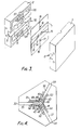
- a microwave switch which is modified in accordance with this invention is illustrated in Figure 3, and it permits the performance level to be substantially enhanced to levels which enable very stringent performance requirements to be met.
- FIG. 3 the reference numerals of Figures 1 and 2 are used to identify like parts.
- the main point of difference shown in Figure 3 comprises two side wall blocks 30 mounted adjacent to the fin line structure (part of the cavity wall is cut away so that one block 30 can be seen, but the other block, which is mounted within the block 3, is not visible).
- Each block has a height which is somewhat less than the corresponding depth of the waveguide channel so that the tops of the blocks do not contact the fin line structure itself.
- Each end of each block 30 is tapered as shown, to give a more gradual transition to and from the slot line mode.
- both blocks 30 are electrically connected to the walls of the channels 6, they can be electrically insulated from it.
- Both blocks 30, are however, formed of a material having a good electrical conductivity.
- Lossy absorbent material 33 and 34 is positioned in each choke cavity to absorb this energy and to prevent the excitation of harmonic modes of any appreciable energy. Similar blocks, not shown, are mounted in the waveguide structure 3 in an exactly analogous manner. Any suitable lossy material can be used, such as Marconi Absorber type Y33-1980.
- the effect of the side wall blocks 30 and the lossy material is to very greatly enhance the performance of the switch.
- the conductivity of the switch in its "on” state remains very high, its effective transmissive impedance in the "off” state becomes very high indeed, and reduces energy leakage to a load of harmonic modes to an extremely low level.
- a three port switch is shown in Figure 4. It has one input port 32, and two output ports 33 and 34.
- the general principle of operation is very similar to that of the switch shown in Figure 3, but three waveguide channels 35, 36, 37 meet at a point where a side wall block 38 is positioned.
- Figure 4 only the bottom half of the switch structure is shown, and in practice an additional block is placed above that of the block 38, 'with a fin line structure between them.
- the block 38 has tapered ends 39, 40, 41.
- the fin line structure is shown in broken line - it consists of three plates 42, 43, 44, with the plates being bridged by switchable diodes 45, 46 placed in the two channels 36, 37 leading to the output ports 33, 34.
- microwave energy can be routed to either output port, or even shared between them.
- Absorbtive (lossy) material 47, 48, 49 is positioned in cavities 50, 51, 52 adjacent to the fin line structure, in a manner analogous to that of Figure 3.
Landscapes
- Waveguide Switches, Polarizers, And Phase Shifters (AREA)
Claims (5)
Priority Applications (2)
| Application Number | Priority Date | Filing Date | Title |
|---|---|---|---|
| EP83302922A EP0126811B1 (de) | 1983-05-20 | 1983-05-20 | Mikrowellenschalter |
| DE8383302922T DE3377760D1 (en) | 1983-05-20 | 1983-05-20 | Microwave switch |
Applications Claiming Priority (1)
| Application Number | Priority Date | Filing Date | Title |
|---|---|---|---|
| EP83302922A EP0126811B1 (de) | 1983-05-20 | 1983-05-20 | Mikrowellenschalter |
Publications (2)
| Publication Number | Publication Date |
|---|---|
| EP0126811A1 EP0126811A1 (de) | 1984-12-05 |
| EP0126811B1 true EP0126811B1 (de) | 1988-08-17 |
Family
ID=8191161
Family Applications (1)
| Application Number | Title | Priority Date | Filing Date |
|---|---|---|---|
| EP83302922A Expired EP0126811B1 (de) | 1983-05-20 | 1983-05-20 | Mikrowellenschalter |
Country Status (2)
| Country | Link |
|---|---|
| EP (1) | EP0126811B1 (de) |
| DE (1) | DE3377760D1 (de) |
Families Citing this family (1)
| Publication number | Priority date | Publication date | Assignee | Title |
|---|---|---|---|---|
| DE3804205A1 (de) * | 1988-02-11 | 1989-08-24 | Licentia Gmbh | Elektrischer hohlleiterschalter |
Family Cites Families (4)
| Publication number | Priority date | Publication date | Assignee | Title |
|---|---|---|---|---|
| US3114119A (en) * | 1959-06-16 | 1963-12-10 | Polytechnic Inst Brooklyn | Hybrid-junction cut-off waveguide filter |
| US3221205A (en) * | 1962-05-23 | 1965-11-30 | Hughes Aircraft Co | Traveling-wave tube with trap means for preventing oscillation at unwanted frequencies |
| FR1600400A (de) * | 1968-12-26 | 1970-07-20 | ||
| FR2511812A1 (fr) * | 1981-08-21 | 1983-02-25 | Thomson Csf | Commutateur d'ondes electromagnetiques |
-
1983
- 1983-05-20 DE DE8383302922T patent/DE3377760D1/de not_active Expired
- 1983-05-20 EP EP83302922A patent/EP0126811B1/de not_active Expired
Non-Patent Citations (1)
| Title |
|---|
| P.J. Meier: "Integrated Fin Line Millimeter Components, IEEE Transactions on Microwave Theory and Techniques, Vol. MTT-22, No. 12, Dec. 1974, pp. 1209-1216 * |
Also Published As
| Publication number | Publication date |
|---|---|
| DE3377760D1 (en) | 1988-09-22 |
| EP0126811A1 (de) | 1984-12-05 |
Similar Documents
| Publication | Publication Date | Title |
|---|---|---|
| US4463330A (en) | Dielectric waveguide | |
| US4689584A (en) | Dielectric slab circulators | |
| US3654573A (en) | Microwave transmission line termination | |
| KR860001644A (ko) | 위상제어 스위칭 장치 | |
| US4034377A (en) | Ferrite circulators and isolators and circuits incorporating the same | |
| US4575701A (en) | Microwave switch | |
| JPH0870206A (ja) | 非放射性誘電体線路部品 | |
| US2577118A (en) | Wave guide filter | |
| JP3045074B2 (ja) | 誘電体線路、電圧制御発振器、ミキサーおよび回路モジュール | |
| US4904966A (en) | Suspended substrate elliptic rat-race coupler | |
| US4568893A (en) | Millimeter wave fin-line reflection phase shifter | |
| US6542046B2 (en) | Directional coupler, antenna device, and radar system | |
| US3851279A (en) | Tee junction waveguide circulator having dielectric matching posts at junction | |
| EP0126811A1 (de) | Mikrowellenschalter | |
| EP0205570B1 (de) | Zusammengestellte dielektrische mehrleiterübertragungsleitung | |
| GB2120460A (en) | Microwave switch | |
| US4151489A (en) | Waveguide switch having four ports and three connecting states | |
| US3721923A (en) | Comprising a slab of semiconductor material | |
| US4507632A (en) | Electromagnetic wave switch | |
| US6380820B1 (en) | Isolator utilizing a planar dielectric transmission line with a resistive film | |
| EP2139063A1 (de) | Hochisolationsschalter mit geringem Verlust und Millimeterwellen | |
| US4660008A (en) | Pin diode switch mounted in a ridge waveguide | |
| CA1243081A (en) | Simple mixer in planar congruently structure | |
| US5317293A (en) | Waveguide switch circuit with improved switching and tuning capability | |
| GB2161990A (en) | Finline with DC-isolated portions |
Legal Events
| Date | Code | Title | Description |
|---|---|---|---|
| PUAI | Public reference made under article 153(3) epc to a published international application that has entered the european phase |
Free format text: ORIGINAL CODE: 0009012 |
|
| 17P | Request for examination filed |
Effective date: 19840724 |
|
| AK | Designated contracting states |
Designated state(s): DE FR IT SE |
|
| 17Q | First examination report despatched |
Effective date: 19860923 |
|
| GRAA | (expected) grant |
Free format text: ORIGINAL CODE: 0009210 |
|
| AK | Designated contracting states |
Kind code of ref document: B1 Designated state(s): DE FR IT SE |
|
| ITF | It: translation for a ep patent filed | ||
| REF | Corresponds to: |
Ref document number: 3377760 Country of ref document: DE Date of ref document: 19880922 |
|
| ET | Fr: translation filed | ||
| ITTA | It: last paid annual fee | ||
| PLBE | No opposition filed within time limit |
Free format text: ORIGINAL CODE: 0009261 |
|
| STAA | Information on the status of an ep patent application or granted ep patent |
Free format text: STATUS: NO OPPOSITION FILED WITHIN TIME LIMIT |
|
| 26N | No opposition filed | ||
| PGFP | Annual fee paid to national office [announced via postgrant information from national office to epo] |
Ref country code: FR Payment date: 19890808 Year of fee payment: 7 |
|
| PGFP | Annual fee paid to national office [announced via postgrant information from national office to epo] |
Ref country code: DE Payment date: 19890811 Year of fee payment: 7 |
|
| PGFP | Annual fee paid to national office [announced via postgrant information from national office to epo] |
Ref country code: SE Payment date: 19901129 Year of fee payment: 8 |
|
| PG25 | Lapsed in a contracting state [announced via postgrant information from national office to epo] |
Ref country code: FR Effective date: 19910131 |
|
| PG25 | Lapsed in a contracting state [announced via postgrant information from national office to epo] |
Ref country code: DE Effective date: 19910201 |
|
| REG | Reference to a national code |
Ref country code: FR Ref legal event code: ST |
|
| PG25 | Lapsed in a contracting state [announced via postgrant information from national office to epo] |
Ref country code: SE Effective date: 19910521 |
|
| EUG | Se: european patent has lapsed |
Ref document number: 83302922.6 Effective date: 19911209 |