EP0126868B1 - Circuit quantificateur-soustracteur - Google Patents
Circuit quantificateur-soustracteur Download PDFInfo
- Publication number
- EP0126868B1 EP0126868B1 EP84102524A EP84102524A EP0126868B1 EP 0126868 B1 EP0126868 B1 EP 0126868B1 EP 84102524 A EP84102524 A EP 84102524A EP 84102524 A EP84102524 A EP 84102524A EP 0126868 B1 EP0126868 B1 EP 0126868B1
- Authority
- EP
- European Patent Office
- Prior art keywords
- transistors
- bias
- analog signal
- analog
- diodes
- Prior art date
- Legal status (The legal status is an assumption and is not a legal conclusion. Google has not performed a legal analysis and makes no representation as to the accuracy of the status listed.)
- Expired - Lifetime
Links
- 230000011664 signaling Effects 0.000 claims 1
- 230000007423 decrease Effects 0.000 description 21
- 238000010586 diagram Methods 0.000 description 6
- 238000006243 chemical reaction Methods 0.000 description 5
- 238000013459 approach Methods 0.000 description 3
- 238000010276 construction Methods 0.000 description 2
- 230000000694 effects Effects 0.000 description 2
- 238000004519 manufacturing process Methods 0.000 description 1
- 230000001681 protective effect Effects 0.000 description 1
- 239000007787 solid Substances 0.000 description 1
Images




Classifications
-
- H—ELECTRICITY
- H03—ELECTRONIC CIRCUITRY
- H03M—CODING; DECODING; CODE CONVERSION IN GENERAL
- H03M1/00—Analogue/digital conversion; Digital/analogue conversion
- H03M1/06—Continuously compensating for, or preventing, undesired influence of physical parameters
- H03M1/0617—Continuously compensating for, or preventing, undesired influence of physical parameters characterised by the use of methods or means not specific to a particular type of detrimental influence
- H03M1/0634—Continuously compensating for, or preventing, undesired influence of physical parameters characterised by the use of methods or means not specific to a particular type of detrimental influence by averaging out the errors, e.g. using sliding scale
- H03M1/0643—Continuously compensating for, or preventing, undesired influence of physical parameters characterised by the use of methods or means not specific to a particular type of detrimental influence by averaging out the errors, e.g. using sliding scale in the spatial domain
- H03M1/0651—Continuously compensating for, or preventing, undesired influence of physical parameters characterised by the use of methods or means not specific to a particular type of detrimental influence by averaging out the errors, e.g. using sliding scale in the spatial domain by selecting the quantisation value generators in a non-sequential order, e.g. symmetrical
Definitions
- the present invention relates to improvements of a quantizer-subtractor circuit of a two-step A/D converter.
- a variety of types of A/D converters have been known. Of those types of A/D converters, the two-step A/D converter has a high-speed performance and a simple construction, as shown in Fig. 1, for example.
- An analog input signal Si is sampled and held by a sample/hold circuit 1.
- the analog input signal Si is sampled and held.
- the held signal is input into a first A/D converter 2 and also into a minus input terminal (-) of a subtractor circuit 3.
- the first A/D converter 2 A/D converts the analog input to digital signals of 3 bits D6, D5, and D4.
- a D/A converter 4 D/A converts the digital signals D6 - D4 and applies the converted ones to a plus input terminal (+) of the subtractor 3.
- a second A/D converter 5 A/D converts the output signal of the subtractor 5 into digital signals of 4 bits D3 - D0.
- the first A/D converter 2 produces digital signals of 3 bits D6 - D4, as shown in Fig. 2(b).
- the D/A converter 4 converts such digital signals derived from the A/D converter 2 to an analog signal and applies it to the subtractor 3.
- the subtractor 3 produces a signal taking a waveform as shown in Fig. 2(c).
- the second A/D converter 5 A/D converts the signal of Fig. 2(c) and produces digital signals D3 - D0 of 4 bits, for example.
- the final A/D converted signal takes the digital form of 7 bits: the three upper bits of the first A/D converter 2 and the four lower bits of the second A/D converter 5.
- a high speed converting operation is ensured when parallel-conversion type A/D converters are used for the A/D converters 2 and 5.
- the number of comparators required when the A/D converting operation is carried out in a two-step fashion, is remarkably reduced as compared with parallel-conversion type A/D converter used in a one-step fashion. Therefore, the total A/D converter is simple in construction.
- a circuit section containing the first A/D converter 2, the D/A converter 4, and the second A/D converter 6 can be simplified into a quantizer-subtractor circuit 6.
- This approach is found in "IEEE JOURNAL OF SOLID - STATE CIRCUITS" VOL. SC - 14, No. 6, DECEMBER 1979, P938 - 943, which discloses a quantizer-subtractor circuit according to the preamble of claim 1.
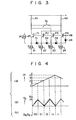
- Fig. 3 is a circuit diagram of the quantizer-subtractor circuit which is shown on page 939, Fig. 2(a) in the above paper.
- Figs. 4(a) and 4(b) correspond to the waveform diagrams of the input current Iin, and subtraction output voltage Vo, as shown in Fig.
- the A/D converted outputs D N and D N-1 encoded are: "00" when the diodes D1 - D3 are all OFF; “01” when the diode D1 is ON, but the diodes D2 and D3 are OFF; “10” when the diodes D1 and D2 are ON, but the diode D3 is OFF; “11” when the diodes D1 - D3 are all ON.
- the subtraction output voltage Vo increases with an increase of the current Iin in the intervals 0 ⁇ Iin ⁇ I and 2I ⁇ Iin ⁇ 3I.
- a couple of the quantizer-subtractor circuits of Fig. 3 may coupled with each other in a parallel fashion, followed by the combination of the encoder and the comparator, as shown in Fig. 3 page 939 in the above paper.
- This alternative arrangement can provide three or more bits of the A/D converter.
- Iin 4I
- the current of 3I flows through the diode D1
- the current of 2I flows through the diode D2
- the current I flows through the diode D3.
- different currents flow through the diodes D1 - D3, respectively. This makes the current densities and the forward voltages of the diodes D1 - D3 different.
- the cutoff point of each of the transistors T2 - T4 changes or fluctuates. Accordingly, the A/D converted outputs D N and D N-1 change at the non-corresponding values of the input current Iin. In other words, the A/D converted output signal does not exactly represent corresponding to a variation of the input current Iin.
- the waveform of the subtraction output voltage Vo is also deformed, as shown in Fig. 4(b), from its exact waveform.
- One of the effective solutions to the cutoff-point shifting problem is to set the forward voltages at equal values. To effect this, the carrier storage effects of the diodes must be set equal to each other.
- the effective junction area of the PN junction finally changes depending on various conditions. For this reason, in manufacturing the diodes, it is very difficult to geometrically change the effective junction area of each diode D1 - D3. Furthermore, when the number of diodes is increased with the increase of the bit number of the A/D conversion, equalizing of the forward voltages of those diodes is made even more difficult.
- prior art document GB-A-2 030 017 which discloses a quantizer-subtractor circuit according to the preamble of claim 1 or 2, describes a circuit arrangement in which the emitters of two transistors are fed from respective direct-current sources and interconnected through a threshold element in the form of a diode.
- diodes are respectively connected between emitters of two transistors in series, and one or two bias voltages are supplied to the basis of the transistors.
- Such an arrangement still has the problem that the values of the currents flowing through the diodes are different. This makes the cutoff point of each of the transistors change or fluctuate, as already explained above.
- the object of the present invention is to provide a quantizer-subtractor circuit which can accurately perform a quantizing and subtracting operation with diodes geometrically equalized in design and manufacutre.
- the present invention provides a quantizer-subtractor circuit as stated in claim 1 or 2.
- the quantizer-subtractor circuit of the present invention successfully overcomes the disadvantages of the prior art, such as the change or fluctuation of the cut-off points of the 2 n transistors. Therefore, the digital outputs after the A/D conversion also take exact values. Further, the current flowing through the load resistor faithfully follows a variation of an input signal, thus securing a highly precise subtraction output, viz., a highly accurate quantizer-subtraction operation. Additionally, in designing a quantizer-subtractor circuit according to the present invention, there is no need to change the effective junction areas of the diodes used to get an improved quantizer-subtracting operation.
- a first transistor Q1 is connected at the collector to a power source Vcc via a load resistor R1, and grounded at the emitter via a first constant current source 31.
- a second transistor Q2 is connected at the collector to the power source Vcc via a load resistor R2, and at the emitter is grounded through a second constant current source 33.
- a third transistor Q3 is connected at the collector to the collector of the first transistor Q1, and at the emitter grounded through a third constant current source 35.
- a fourth transistor Q4 is connected at the collector to the collector of the second transistor Q2, and at the emitter grounded by way of a fourth constant current source 37.
- a positive output terminal of a bias power source with voltage VB is connected to the base of the transistor Q4 and grounded through a bias circuit 47 formed by a series circuit containing four to six diodes 39, 41 and 43 and a fifth constant current source 45.
- a junction of the diode 39 and the fifth constant current source 45 is connected to the base of the transistor Q1.
- a junction of the diodes 39 and 41 is connected to the base of the transistor Q2.
- a junction of the diodes 41 and 43 is connected to the base of the transistor Q3.
- the output terminal of the analog input constant current source 25 is directly connected to the emitter of the first transistor Q1, and to the emitter of the second transistor Q2 via a first diode 49.
- the same output terminal is connected via a second diode 51 to the emitter of the third transistor Q3, and to the emitter of the fourth transistor Q4 via a third diode 53. Further, the output terminal is connected to the base of the fourth transistor Q4 via a protective diode 55.
- the anode of the first diode 49 is connected to the positive input terminal of a comparator 57, and its cathode is connected to a negative input terminal.
- the output terminal of the comparator 57 is connected to the input terminal I1 of an encoder 63.
- the anode of the second diode 51 is connected to the positive input terminal of a comparator 59, and its cathode is connected to a negative input terminal of the comparator 59.
- the comparator 59 is connected at the output terminal to the input terminal I2 of the encoder 63.
- the anode of the third diode 53 is connected to the positive input terminal of the comparator 61.
- the cathode of the third diode 53 is coupled with the negative input terminal of the comparator 61.
- the output terminal of the comparator 61 is connected to the input terminal I3 of the encoder 63.
- the subtraction output voltage Vo represents the difference in voltage between the output terminal N1 connecting to a junction among the collectors of the first and third transistors Q1 and Q3, and the output terminal N2 connecting to a junction of the collectors of the second and fourth transistors Q2 and Q4.
- the resistors R1 and R2 have equal resistance values R.
- the current value of each of the constant current sources 31, 33, 35, 37 and 45 is I.
- the operation of the quantizer-subtractor circuit will be described referring to Figs. 6(a) - 6(g).
- the analog input constant current source 25 produces an input current Iin proportional to an analog input signal.
- the description of the operation to follows is limited within a specific interval 0 to 4I of a rectangular wave of the input current Iin shown in Fig. 6(a), for simplicity.
- an L level signal is input to the input terminals I1 to I3 of the encoder 63, which in turn produces a digital signal "00".
- the emitter potential of the first transistor Q1 is 1 V
- VBE is the voltage between the base and emitter of the transistor of NPN type.
- VF is a forward voltage drop of the diode.
- the input current Iin flows into the first constant current source 31 connected to the lowest emitter potential point. With an increase in the input current Iin, the current flowing through the collector-emitter path of the first transistor Q1 decreases. The current of the resistor R1 also decreases. Then, the voltage drop of the resistor R1 decreases, and the voltage at the output terminal N1 increases. The current of the resistor R2 remains unchanged. This means that the voltage at the output terminal N2 is constant. Therefore, the subtraction output voltage Vo rises, as shown in Fig. 6(b). Also in this case, since no current flows into the first to third diodes 49, 51 and 53, no voltage drop is generated across each diodes 49, 51 and 53. As shown in Figs. 6(c) - 6(e), the output signals of the comparators 57, 59 and 61 are at L level. As a consequence, the encoder 63 produces a digital signal of "00".
- a portion I of the input current Iin flows into the constant current source 31. The result is that no current flows into the collector-emitter path of the first transistor Q1, and the transistor Q1 is turned off.
- the current (Iin - I) flows into the second constant current source 33, via the first diode 49 connecting to the lowest potential point of emitter potentials of the transistors Q2 - Q4.
- the current of the second transistor Q2 and the resistor R2 decreases with the increase of the current Iin.
- the voltage drop across the resistor R2 decreases and the voltage at the terminal N2 rises.
- the voltage drop across the resistor R1 is unchanged, and the voltage at the output terminal N1 is constant. Therefore, the subtraction output voltage Vo gradually decreases as shown in Fig.
- a portion I of the input current Iin flows to the constant current source 31 and another portion I flows to the constant current source 33. Then, the first and second transistors Q1 and Q3 are cut off.
- the emitter potential of the third transistor Q3 is lower than that of the fourth transistor Q4. Accordingly, current Iin - 2I flows into the constant current source 35 via the diode 51 connected to the emitter of the third transistor Q3.
- the current of the collector-emitter path of the third transistor Q3 decreases. The result is a decrease in the current flowing through the resistor R1 and in the voltage drop across the resistor R1. Further, the voltage at the output terminal N1 rises.
- portion I of the input current Iin flows to the constant current source 31, portion I flows to the constant current source 33 and portion I flows to the constant current source 35.
- the transistor Q3 is also turned off in addition to the first and second transistors Q1 and Q2.
- the remaining current (Iin - 3I) flows into the fourth constant current source 37, through the third diode 53. Accordingly, with an increase of the input current Iin, the current flowing through the collector-emitter path of the transistor Q4 decreases. The result is that the current of the resistor R2 decreases and the voltage drop across the resistor R2 decreases. Then, the voltage at the output terminal N2 rises.
- the current of the resistor R1 is constant and the voltage at the output terminal N1 is constant.
- the subtraction output voltage Vo decreases as shown in Fig. 6(b).
- the current flows into the first, second and third diodes 49, 51 and 53, causing the voltage drop.
- the comparators 57, 59 and 61 detect these voltage drops and produce H level signals, as shown in Figs. 6(c) - 6(e).
- the encoder 63 produces logical signals "11", as shown in Fig. 6(f).
- the 2-bit digital signals are obtained.
- the subtraction output voltage Vo corresponds to the difference between the value of the analog signal and the value corresponding to the output digital signal.
- the subtraction output thus obtained is similar to that of the quantizer-subtractor circuit shown in Fig. 3. For this reason, when the subtraction output Vo, after it is A/D converted, is used as the lower bits, those bits must logically be inverted during the period where the subtraction output voltage Vo decreases with the increase of the input current Iin, viz., in the interval where the digital signals derived from the encoder 63 are "01" and "11".
- the peak values of the currents I flowing into the diodes 49, 51 and 53, which are connected correspondingly to the emitters of the second to fourth transistors Q2 - Q4, are equal to each other.
- This fact implies that the characteristics of the diodes and the transistors as well are set equal to each other, and that the circuit design is simplified.
- the current flowing through each resistor R1 and R2 exactly changes by I against a change of the input current Iin for each interval 0 - I, I - 2I, 2I - 3I, and 3I - 4I.
- a high-precision quantizer-subtractor circuit is provided.
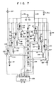
- a quantizer-subtractor circuit capable of producing 3-bit digital signals is illustrated in Fig. 7.
- emitters of the transistors 71, 73, 75, 77, 79, 81, 83 and 85 are respectively connected to constant current sources 89, 91, 93, 95, 97, 99, 101 and 103.
- the bases of those transistors are respectively connected to a bias circuit 105 so as to be applied with different bias voltages.
- the collectors of the transistors 71, 75, 79 and 83 are connected together to a first load resistor R1.
- the collectors of the transistors 73, 77, 81 and 85 are connected together to a second load resistor R2.
- the output terminal of the input constant current source 107 for producing the current corresponding to the analog input signal is directly connected to the emitter of the transistor 71, and to the emitters of the transistors 73, 75, 77, 79, 81, 83 and 85 by way of the diodes 111, 113, 115, 117, 119, 121 and 123.
- Plus input terminals and minus input terminals of the comparators 125, 127, 129, 131, 133, 135 and 137 are connected to the anode and the cathodes of those diodes 111, 113, 115, 117, 119 121 and 123 respectively, as shown.
- the output terminals of those comparators are connected to the input terminals of an encoder 139.
- the output signal from the encoder 139 are used as the digital output signals.
- the subtraction output voltage Vo represents a potential difference between the output terminal N1 connected to the first load resistor R1 and the output terminal N2 connected to the second load resistor R2.
- the diode 141 is provided for protection purposes.
- a quantizer-subtractor circuit capable of producing n-bit digital signals, which uses NPN type components will now be given.
- Constant current sources are respectively connected to the emitters of 2 n transistors. Different bias voltages are applied to the bases of those 2 n transistors. This is realized by using a bias circuit (similar to bias circuit 47 shown in Fig. 5) comprised of a plurality of diodes and the constant current source in series connected to each other. It is as a matter of course that any other known bias circuits are available for this bias circuit.
- the collectors of the transistors to which the bias voltages with odd-ordered magnitudes are applied are connected together to the first load resistor.
- the collectors of the transistors to which the bias voltages with the even-ordered magnitudes are applied are connected together to the second load resistor.
- the output terminal of the input constant current source is directly connected to the emitter of the transistor to which the smallest bias voltage is applied, and is connected to the each emitter of the remaining (2 n - 1) transistors via the diode.
- Plus input terminals and minus input terminals of the comparators are respectively connected to the anodes and the cathodes of the (2 n - 1) diodes connecting to the emitters of the transistors.
- the comparators detect the voltages between the cathodes and the anodes of the (2 n - 1) diodes.
- the output terminals of the comparators are connected to the input terminals of an encoder.
- the output signals of the comparators are input to the encoder with (2 n - 1) input terminals.
- the subtraction output voltage is produced in the form of the potential difference between the junction of the first load resistor and the transistors, and a junction of the second load resistor and the transistors.
- Fig. 8 illustrating a quantizer-subtractor circuit with 2-bit digital output signals, which uses PNP transistors.
- constant current sources 159, 161, 163 and 165 are respectively connected to transistors 151, 153, 155 and 157.
- the bases of the transistors 151, 153, 155 and 157 are respectively connected to a bias circuit 175 composed of diodes 167, 169 and 171, and a constant current source 173.
- the collectors of the transistors 151 and 155 are connected together to the first load resistor R1.
- the collectors of the transistors 153 and 157 are connected to a second load resistor.
- the input terminal of the input current source 169 is directly connected to the emitter of the transistor 151. The same is connected via diodes 171, 173 and 175 to the emitters of the transistors 153, 155 and 157.
- the input terminals of the comparators 179, 181 and 183 detect respectively the voltages between the anodes and the cathodes of the diodes 171, 173 and 175.
- the output terminals of the comparators 179, 181 and 183 are respectively connected to the input terminals of the encoder 185.
- the output of the encoder 185 is used as a digital output.
- the subtraction output voltage Vo is the potential difference between the output terminal N1 which is connected to the first load resistor R1 and the output terminal N2 which is connected to the second load resistor R2.
- Constant current sources are connected to the emitters of 2 n transistors. Different bias voltages are applied to the bases of those transistors.
- the collectors of the transistors to which the bias voltages with odd-ordered magnitudes are applied are connected together to the first load resistor.
- the collectors of the transistors to which the bias voltages with the even-ordered magnitudes are applied are connected together to the second load resistor.
- the output terminal of the input constant current source is directly connected to the emitter of the transistor to which the largest bias voltage is applied.
- the input terminal of the input constant current source is connected to each emitter of the remaining transistors via the diode.
- Plus input terminal and minus input terminals of the comparators are connected to the anodes and the cathodes of the (2 n - 1) diodes connecting the emitters of the transistors.
- the comparators detect the voltages between the cathodes and the anodes of the diodes, and input them to the encoder with (2 n - 1) input terminals.
- the subtraction output voltage Vo is produced in the form of the potential difference between the junction of the first load resistor and the transistors, and a junction of the second load resistor and the transistors.
- the voltage drops across the diodes which are connected to the emitters of the transistors are detected by the comparators.
- the detected voltage drops are encoded by the encoder to have digital output signals. It should be understood that the present invention is not limited to this.
- the digital output can be obtained by checking as to whether or not the currents flowing into the transistors each have a predetermined value I.
- An additional A/D converter may be provided and selected as needed.
- the analog input current source is not always needed. For example, when the input signal takes the form of a current signal, the analog input current source is unnecessary.
Landscapes
- Engineering & Computer Science (AREA)
- Theoretical Computer Science (AREA)
- Analogue/Digital Conversion (AREA)
Claims (5)
- Circuit quantificateur soustracteur comprenant des moyens d'entrée (25) de signal analogique pour saisir en entrée un signal d'entrée analogique, des moyens de sortie (57 à 63) de signal numérique pour produire un signal numérique correspondant au dit signal d'entrée analogique entré sur lesdits moyens d'entrée (25) de signal analogique, et des moyens de sortie de signal analogique pour produire un signal analogique (V0) à titre de sortie de soustraction correspondant à la différence entre la valeur dudit signal d'entrée analogique entré par lesdits moyens d'entrée (25) de signal analogique et la valeur correspondante à la sortie de signal analogique produite par lesdits moyens de sortie de signal numérique (57 à 63), dans lequel lesdits moyens de sortie de signal analogique comportent :
2n transistors (Q1 à Q4) de type NPN, n étant un entier supérieur ou égal à 2 ;
des moyens de polarisation (47) connectés aux bases desdits 2n transistors (Q1 à Q4) de type NPN et pour fournir des tensions de polarisation aux bases desdits transistors NPN (Q1 à Q4) ;
2n sources à courant constant (31 à 37) respectivement connectées aux émetteurs desdits 2n transistors (Q1 à Q4) de type NPN ;
un circuit pour connecter lesdits moyens d'entrée de signal analogique (25) à un émetteur d'un transistor NPN sur lequel est appliqué une tension de polarisation appliquée par lesdits moyens de polarisation (47) ;
(2n-1) diodes (49 à 53) qui sont respectivement connectées par leurs cathodes aux émetteurs des (2n-1) transistors (Q2 à Q4), et
des moyens de production de signal analogique (R1, R2, N1 et N2) pour produire un signal analogique correspondant à la différence entre la valeur totale des courants circulant à travers les transistors (Q1, Q3) desdits 2n transistors, qui sont alimentés par les tensions de polarisation d'amplitudes d'ordres impairs appliquées par lesdits moyens de polarisation (47) et la valeur totale des courants circulant à travers les transistors (Q2, Q4) desdits 2n transistors (Q1 à Q4), qui sont alimentés par les tensions de polarisation d'amplitudes d'ordres pairs appliquées par lesdits moyens de polarisation (47) de façon à ce que :- lesdits moyens de polarisation (47) fournissent des tensions de polarisation différentes aux bases des 2n transistors (Q1 à Q4) de type NPN ;
caractérisé en ce que :- lesdits moyens de polarisation comportent une source (45) à courant constant connectée en série aux dits moyens d'entrée (25) de signal analogique, et une pluralité de diodes (39, 41, 43) connectées en série dans le même sens entre lesdits moyens d'entrée de signal analogique (25) et ladite source à courant constant (45) pour fournir des tensions de polarisation de valeurs différentes aux bases desdits 2n transistors (Q1 à Q4) de type NPN ;- ledit circuit de connexion connecte les moyens d'entrée (25) de signal analogique à l'émetteur du transistor NPN sur lequel est appliqué la plus basse des tensions de polarisation appliquées par lesdits moyens de polarisation (47) ; et- lesdites (2n-1) diodes (49 à 53) sont respectivement connectées par les cathodes aux émetteurs des (2n-1) transistors (Q2 à Q4) autres que ledit transistor (Q1) sur lequel est appliquée la plus basse des tensions de polarisation et connectées par les anodes aux dits moyens d'entrée (25) (figure 5) de signal analogique. - Circuit quantificateur soustracteur comprenant des moyens d'entrée (169) de signal analogique pour saisir en entrée un signal d'entrée analogique, des moyens de sortie (178 à 185) de signal numérique pour produire un signal numérique correspondant au dit signal d'entrée analogique entré sur lesdits moyens d'entrée (169) de signal analogique, et des moyens de sortie de signal analogique pour produire un signal analogique (V0) à titre de sortie de soustraction correspondant à la différence entre la valeur dudit signal d'entrée analogique entré par lesdits moyens d'entrée (160) de signal analogique et la valeur correspondante à la sortie de signal numérique produite par lesdits moyens de sortie de signal numérique (178 à 185), dans lequel lesdits moyens de sortie de signal analogique comportent :
2n transistors (151 à 157) de type PNP, n étant un entier supérieur ou égal à 2 ;
des moyens de polarisation (175) connectés aux bases desdits 2n transistors (151 à 157) de type PNP et pour fournir des tensions de polarisation aux bases desdits transistors NPN (151 à 157) ;
2n sources à courant constant (159, 161, 163, 165) respectivement connectées aux émetteurs desdits 2n transistors (151 à 157) de type PNP ;
un circuit pour connecter lesdits moyens d'entrée de signal analogique (169) à un émetteur d'un transistor (151) PNP sur lequel est appliqué une tension de polarisation appliquée par lesdits moyens de polarisation (175) ;
(2n -1) diodes (171 à 175) qui sont respectivement connectées par leurs cathodes aux émetteurs des (2n-1) transistors (153 à 157), et
des moyens de production de signal analogique (R1, R2, N1 et N2) pour produire un signal analogique correspondant à la différence entre la valeur totale des courants circulant à travers les transistors (151 à 155) desdits 2n transistors, qui sont alimentés par les tensions de polarisation d'amplitudes d'ordres impairs appliquées par lesdits moyens de polarisation (175) et la valeur totale des courants circulant à travers les transistors (153, 157) desdits 2n transistors qui sont alimentés par les tensions de polarisation d'amplitudes d'ordres pairs appliquées par lesdits moyens de polarisation (175) de façon à ce que :- lesdits moyens de polarisation (175) fournissent diverses tensions de polarisation aux bases des 2n transistors (151 à 157) de type PNP ;
caractérisé en ce que :- lesdits moyens de polarisation (175) comportent une source (173) à courant constant connectée en série aux dits moyens d'entrée (169) de signal analogique, et une pluralité de diodes (167, 169, 171) connectées en série dans le même sens entre lesdits moyens d'entrée de signal analogique (169) et ladite source à courant constant (173) pour fournir des tensions de polarisation de valeurs différentes aux bases desdits 2n transistors (151, 153, 155, 157) de type PNP ;- ledit circuit de connexion connecte les moyens d'entrée (169) de signal analogique à l'émetteur du transistor NPN (151) sur lequel est appliqué la plus haute des tensions de polarisation appliquées par lesdits moyens de polarisation (175) ; et- lesdites (2n-1) diodes (171 à 175) sont respectivement connectées par les cathodes aux émetteurs des (2n-1) transistors (153 à 157) autres que ledit transistor (151) sur lequel est appliqué la plus haute des tensions de polarisation et connectées par les anodes aux dits moyens d'entrée (169) (figure 8) de signal analogique. - Circuit quantificateur soustracteur selon la revendication 1 ou 2, caractérisé en ce que lesdits moyens de production (R1, R2, N1 et N2) de signal analogique comportent une première résistance (R1) connectée aux collecteurs des premiers transistors (Q1, Q3 ; 151, 155) desdits 2n transistors, qui reçoivent des tensions de polarisation d'amplitudes d'ordres impairs appliquées par lesdits moyens de polarisation (47 ; 175), une seconde résistance (R2) connectée aux collecteurs des seconds transistors (Q2, Q4 ; 153, 157) des dits 2n transistors qui sont alimentés par lesdites tensions de polarisation d'ordres pairs appliquées par lesdits moyens de polarisation (47 ; 175), une première borne de sortie (N1) connectée à un point de connexion sur lequel ladite première résistance (R1) et les collecteurs desdits premiers transistors (Q1, Q3 ; 151, 155) sont connectés, et une seconde borne de sortie (N2) connectée à un point de connexion (N2) sur lequel ladite seconde résistance (R2) et les collecteurs desdits seconds transistors (Q2, Q4 ; 153, 157) sont connectés.
- Circuit quantificateur soustracteur selon la revendication 1 ou 2 , caractérisé en ce que lesdits moyens de sortie (57 à 63 ; 178 à 185) de signal numérique comportent des moyens de détection pour détecter les courants circulant à travers lesdites (2n-1) diodes (49, 51 et 53 ; 171, 173 et 175) constituant des moyens de commande, et des moyens (63 ; 185) pour fournir en sortie un signal numérique sur la base des courants détectés par lesdits moyens de détection.
- Circuit quantificateur soustracteur selon la revendication 1 ou 2 , caractérisé en ce que lesdits moyens d'entrée de signal analogique comportent des moyens de sortie (25 ; 169) de courant analogique pour produire un courant d'entrée analogique correspondant au dit signal d'entrée analogique, et
des moyens de commande (31, 33, 49, 35, 51, 37, 53) (159, 161, 171, 163, 173, 165, 175) constitués par lesdites 2n sources (31, 33, 35, 37 ; 159, 161, 163, 153) à courant constant et par lesdites 2n-1 diodes (49, 51, 53 ; 171, 173, 175) commandent le courant circulant à travers le chemin émetteur- collecteur de chacun desdits 2n transistors (Q1 - Q4 ; 151 à 157) correspondant à ladite sortie de signal d'entrée analogique provenant desdits moyens d'entrée (25 ; 169) de signal analogique et aux dites tensions de polarisation appliquées aux bases desdits 2n transistors (Q1 à Q4 ; 151 à 157) par lesdits moyens de polarisation (47, 175).
Applications Claiming Priority (2)
| Application Number | Priority Date | Filing Date | Title |
|---|---|---|---|
| JP54302/83 | 1983-03-30 | ||
| JP58054302A JPS59178820A (ja) | 1983-03-30 | 1983-03-30 | 量子化・減算回路 |
Publications (3)
| Publication Number | Publication Date |
|---|---|
| EP0126868A2 EP0126868A2 (fr) | 1984-12-05 |
| EP0126868A3 EP0126868A3 (en) | 1988-05-11 |
| EP0126868B1 true EP0126868B1 (fr) | 1992-05-20 |
Family
ID=12966772
Family Applications (1)
| Application Number | Title | Priority Date | Filing Date |
|---|---|---|---|
| EP84102524A Expired - Lifetime EP0126868B1 (fr) | 1983-03-30 | 1984-03-08 | Circuit quantificateur-soustracteur |
Country Status (4)
| Country | Link |
|---|---|
| US (1) | US4584557A (fr) |
| EP (1) | EP0126868B1 (fr) |
| JP (1) | JPS59178820A (fr) |
| DE (1) | DE3485731D1 (fr) |
Family Cites Families (3)
| Publication number | Priority date | Publication date | Assignee | Title |
|---|---|---|---|---|
| BE487541A (fr) * | 1948-02-26 | |||
| NL7609608A (nl) * | 1976-08-30 | 1978-03-02 | Philips Nv | Analoog-digitaal omzetter. |
| NL7808871A (nl) * | 1978-08-29 | 1980-03-04 | Philips Nv | Analoog-digitaal omzetter. |
-
1983
- 1983-03-30 JP JP58054302A patent/JPS59178820A/ja active Pending
-
1984
- 1984-03-07 US US06/587,128 patent/US4584557A/en not_active Expired - Lifetime
- 1984-03-08 EP EP84102524A patent/EP0126868B1/fr not_active Expired - Lifetime
- 1984-03-08 DE DE8484102524T patent/DE3485731D1/de not_active Expired - Lifetime
Non-Patent Citations (1)
| Title |
|---|
| IEEE Journal of Solid-State Circuits, Vol. Sc-14, No. 6, Dec. 1979, pages 938-943 * |
Also Published As
| Publication number | Publication date |
|---|---|
| JPS59178820A (ja) | 1984-10-11 |
| EP0126868A3 (en) | 1988-05-11 |
| US4584557A (en) | 1986-04-22 |
| DE3485731D1 (de) | 1992-06-25 |
| EP0126868A2 (fr) | 1984-12-05 |
Similar Documents
| Publication | Publication Date | Title |
|---|---|---|
| US4642551A (en) | Current to voltage converter circuit | |
| US4179687A (en) | Analog-to-digital converter circuit employing iterative subtraction | |
| US5719578A (en) | Folding amplifier for the construction of an A/D converter | |
| US3858199A (en) | Tracking level detector | |
| JPH0754910B2 (ja) | Ad変換器 | |
| US4706010A (en) | Linear solar array voltage control system | |
| EP0028454B1 (fr) | Redresseur biphasé | |
| US5313207A (en) | Differential subtracter improved for higher accuracy and A/D converter including the same | |
| US4362956A (en) | Absolute value circuit | |
| CA1055613A (fr) | Convertisseur analogique/numerique | |
| US4325054A (en) | Folding circuit for an analog-to-digital converter | |
| JPS63114410A (ja) | データ整形回路 | |
| US4651033A (en) | Device for complementary input signals using two circuits with different threshold voltages | |
| US4584557A (en) | Quantizer-subtractor circuit | |
| KR920010216B1 (ko) | A/d 변환기의 바이어스회로 | |
| US4124844A (en) | Analog to digital converter having a high speed subtraction circuit | |
| US4401974A (en) | Digital sample and hold circuit | |
| US3717777A (en) | Digital to analog converter including improved reference current source | |
| US5774086A (en) | Voltage amplifier having a large range of variations, and A/D converter comprising such an amplifier | |
| US4945301A (en) | Constant-voltage power supply circuit and amplifier circuit and DA converter using the constant-voltage power supply circuit | |
| EP0096442B1 (fr) | Convertisseur analogique-numérique de courant | |
| US4961045A (en) | Floating output digital to analog converter | |
| US4758820A (en) | Semiconductor circuit | |
| KR950010210B1 (ko) | 전자 회로 및 아나로그 대 디지탈 컨버터 | |
| US4739192A (en) | Fast settling digital to analog converter bit switch |
Legal Events
| Date | Code | Title | Description |
|---|---|---|---|
| PUAI | Public reference made under article 153(3) epc to a published international application that has entered the european phase |
Free format text: ORIGINAL CODE: 0009012 |
|
| 17P | Request for examination filed |
Effective date: 19840404 |
|
| AK | Designated contracting states |
Designated state(s): DE FR GB |
|
| XX | Miscellaneous (additional remarks) |
Free format text: EIN ANTRAG NACH REGEL 88 EPUE AUF BERICHTIGUNG DER BESCHREIBUNG UND DER PATENTANSPRUECHE WURDE AM 20.08.1984 EINGEREICHT. |
|
| PUAL | Search report despatched |
Free format text: ORIGINAL CODE: 0009013 |
|
| AK | Designated contracting states |
Kind code of ref document: A3 Designated state(s): DE FR GB |
|
| 17Q | First examination report despatched |
Effective date: 19890803 |
|
| GRAA | (expected) grant |
Free format text: ORIGINAL CODE: 0009210 |
|
| AK | Designated contracting states |
Kind code of ref document: B1 Designated state(s): DE FR GB |
|
| XX | Miscellaneous (additional remarks) |
Free format text: EIN ANTRAG NACH REGEL 88 EPUE AUF BERICHTIGUNG DER BESCHREIBUNG UND DER PATENTANSPRUECHE WURDE AM 20.08.1984 EINGEREICHT. |
|
| REF | Corresponds to: |
Ref document number: 3485731 Country of ref document: DE Date of ref document: 19920625 |
|
| ET | Fr: translation filed | ||
| PLBE | No opposition filed within time limit |
Free format text: ORIGINAL CODE: 0009261 |
|
| STAA | Information on the status of an ep patent application or granted ep patent |
Free format text: STATUS: NO OPPOSITION FILED WITHIN TIME LIMIT |
|
| 26N | No opposition filed | ||
| PGFP | Annual fee paid to national office [announced via postgrant information from national office to epo] |
Ref country code: GB Payment date: 19980227 Year of fee payment: 15 |
|
| PGFP | Annual fee paid to national office [announced via postgrant information from national office to epo] |
Ref country code: FR Payment date: 19980310 Year of fee payment: 15 |
|
| PGFP | Annual fee paid to national office [announced via postgrant information from national office to epo] |
Ref country code: DE Payment date: 19980313 Year of fee payment: 15 |
|
| PG25 | Lapsed in a contracting state [announced via postgrant information from national office to epo] |
Ref country code: GB Free format text: LAPSE BECAUSE OF NON-PAYMENT OF DUE FEES Effective date: 19990308 |
|
| GBPC | Gb: european patent ceased through non-payment of renewal fee |
Effective date: 19990308 |
|
| PG25 | Lapsed in a contracting state [announced via postgrant information from national office to epo] |
Ref country code: FR Free format text: LAPSE BECAUSE OF NON-PAYMENT OF DUE FEES Effective date: 19991130 |
|
| REG | Reference to a national code |
Ref country code: FR Ref legal event code: ST |
|
| PG25 | Lapsed in a contracting state [announced via postgrant information from national office to epo] |
Ref country code: DE Free format text: LAPSE BECAUSE OF NON-PAYMENT OF DUE FEES Effective date: 20000101 |