EP0127089B1 - Halbleiterelement mit zwei Elektroden und Verfahren zu seiner Herstellung - Google Patents
Halbleiterelement mit zwei Elektroden und Verfahren zu seiner Herstellung Download PDFInfo
- Publication number
- EP0127089B1 EP0127089B1 EP84105669A EP84105669A EP0127089B1 EP 0127089 B1 EP0127089 B1 EP 0127089B1 EP 84105669 A EP84105669 A EP 84105669A EP 84105669 A EP84105669 A EP 84105669A EP 0127089 B1 EP0127089 B1 EP 0127089B1
- Authority
- EP
- European Patent Office
- Prior art keywords
- substrate
- alloy layer
- surface electrode
- layer
- semiconductor device
- Prior art date
- Legal status (The legal status is an assumption and is not a legal conclusion. Google has not performed a legal analysis and makes no representation as to the accuracy of the status listed.)
- Expired - Lifetime
Links
Images


Classifications
-
- H—ELECTRICITY
- H10—SEMICONDUCTOR DEVICES; ELECTRIC SOLID-STATE DEVICES NOT OTHERWISE PROVIDED FOR
- H10W—GENERIC PACKAGES, INTERCONNECTIONS, CONNECTORS OR OTHER CONSTRUCTIONAL DETAILS OF DEVICES COVERED BY CLASS H10
- H10W20/00—Interconnections in chips, wafers or substrates
- H10W20/40—Interconnections external to wafers or substrates, e.g. back-end-of-line [BEOL] metallisations or vias connecting to gate electrodes
-
- H—ELECTRICITY
- H10—SEMICONDUCTOR DEVICES; ELECTRIC SOLID-STATE DEVICES NOT OTHERWISE PROVIDED FOR
- H10W—GENERIC PACKAGES, INTERCONNECTIONS, CONNECTORS OR OTHER CONSTRUCTIONAL DETAILS OF DEVICES COVERED BY CLASS H10
- H10W72/00—Interconnections or connectors in packages
-
- H—ELECTRICITY
- H10—SEMICONDUCTOR DEVICES; ELECTRIC SOLID-STATE DEVICES NOT OTHERWISE PROVIDED FOR
- H10W—GENERIC PACKAGES, INTERCONNECTIONS, CONNECTORS OR OTHER CONSTRUCTIONAL DETAILS OF DEVICES COVERED BY CLASS H10
- H10W72/00—Interconnections or connectors in packages
- H10W72/01—Manufacture or treatment
- H10W72/012—Manufacture or treatment of bump connectors, dummy bumps or thermal bumps
-
- H—ELECTRICITY
- H10—SEMICONDUCTOR DEVICES; ELECTRIC SOLID-STATE DEVICES NOT OTHERWISE PROVIDED FOR
- H10W—GENERIC PACKAGES, INTERCONNECTIONS, CONNECTORS OR OTHER CONSTRUCTIONAL DETAILS OF DEVICES COVERED BY CLASS H10
- H10W72/00—Interconnections or connectors in packages
- H10W72/20—Bump connectors, e.g. solder bumps or copper pillars; Dummy bumps; Thermal bumps
- H10W72/251—Materials
-
- H—ELECTRICITY
- H10—SEMICONDUCTOR DEVICES; ELECTRIC SOLID-STATE DEVICES NOT OTHERWISE PROVIDED FOR
- H10W—GENERIC PACKAGES, INTERCONNECTIONS, CONNECTORS OR OTHER CONSTRUCTIONAL DETAILS OF DEVICES COVERED BY CLASS H10
- H10W72/00—Interconnections or connectors in packages
- H10W72/20—Bump connectors, e.g. solder bumps or copper pillars; Dummy bumps; Thermal bumps
- H10W72/29—Bond pads specially adapted therefor
-
- H—ELECTRICITY
- H10—SEMICONDUCTOR DEVICES; ELECTRIC SOLID-STATE DEVICES NOT OTHERWISE PROVIDED FOR
- H10W—GENERIC PACKAGES, INTERCONNECTIONS, CONNECTORS OR OTHER CONSTRUCTIONAL DETAILS OF DEVICES COVERED BY CLASS H10
- H10W72/00—Interconnections or connectors in packages
- H10W72/50—Bond wires
- H10W72/59—Bond pads specially adapted therefor
-
- H—ELECTRICITY
- H10—SEMICONDUCTOR DEVICES; ELECTRIC SOLID-STATE DEVICES NOT OTHERWISE PROVIDED FOR
- H10W—GENERIC PACKAGES, INTERCONNECTIONS, CONNECTORS OR OTHER CONSTRUCTIONAL DETAILS OF DEVICES COVERED BY CLASS H10
- H10W72/00—Interconnections or connectors in packages
- H10W72/90—Bond pads, in general
- H10W72/951—Materials of bond pads
- H10W72/952—Materials of bond pads comprising metals or metalloids, e.g. PbSn, Ag or Cu
-
- Y—GENERAL TAGGING OF NEW TECHNOLOGICAL DEVELOPMENTS; GENERAL TAGGING OF CROSS-SECTIONAL TECHNOLOGIES SPANNING OVER SEVERAL SECTIONS OF THE IPC; TECHNICAL SUBJECTS COVERED BY FORMER USPC CROSS-REFERENCE ART COLLECTIONS [XRACs] AND DIGESTS
- Y10—TECHNICAL SUBJECTS COVERED BY FORMER USPC
- Y10S—TECHNICAL SUBJECTS COVERED BY FORMER USPC CROSS-REFERENCE ART COLLECTIONS [XRACs] AND DIGESTS
- Y10S438/00—Semiconductor device manufacturing: process
- Y10S438/928—Front and rear surface processing
Definitions
- the present invention relates to a semiconductor device, a method of producing the same, particularly a device including:
- the back surface electrode is formed from a gold antimony alloy deposited onto a silicon substrate and then heat treated to form a eutectic alloy between the back electrode and the silicon substrate.
- This citation does not teach the method of forming a back surface electrode without a heat treatment step.
- a glass sealed diode as shown in Fig. 1 is known as a semiconductor device provided with two terminals. It is seen that a semiconductor device 1, i.e. a diode, is housed in a glass container 2 which is held between jumets 3, 3. Lead wires 4, 4 are connected to the device 1 via the jumets 3, 3.
- a semiconductor device of this type comprises a semiconductor substrate provided with at least two semiconductor regions and front and back surface electrodes mounted on the front and back surfaces of the substrate.
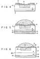
- Figs. 2-6 collectively show a method of producing a semiconductor device of this type.
- a semiconductor substrate 5 comprising an N +- region and an N-region formed on the N +- regioh is subjected to thermal oxidation to form insulation films 6 on both surfaces of the substrate.
- an opening 7 is made in the insulation film 6 on the front surface of the substrate, i.e., on the N-region, followed by diffusing a P-type impurity through the opening 7 into the substrate to form a P +- region within the N-region, as shown in Fig. 2.
- the insulation film on the back surface of the substrate 5 is removed by selective etching. As shown in Fig.
- a thin insulation film 8 is formed on the insulation film 6 on the front surface and on the exposed substrate surface, followed by polishing the N +- region on the back side of the substrate 5 to a prescribed extent.
- the polishing is intended to control the depth of the N* -region. In some cases, the thickness of the substrate is reduced to nearly half the original thickness by the polishing treatment.
- a nickel layer is formed on the back surface of the substrate by an electroplating method, followed by sintering the nickel layer at about 700°C for 10 minutes so as to form a sintered nickel layer 9 comprising a nickel/ semiconductor substrate alloy as shown in Fig. 4.
- Fig. 4 also shows a front surface electrode 10, which is formed by making a hole in the thin insulation layer 8 positioned on the P +- impurity region by selective etching, followed by vapour deposition of a gold alloy and subsequent selective etching of the gold alloy. Then, a silver bumper 11 is formed to cover the front surface electrode 10 as shown in Fig. 5. Further, a nickel layer 12, a gold layer 13, and a silver layer 14 are formed by an electroplating in the order mentioned on the sintered nickel layer 9 so to form a back surface electrode.
- the substrate is subjected to a pretreatment such as a water wash, followed by applying a silver plating to the substrate.
- a pretreatment such as a water wash
- the substrate and a silver plate immersed in the plating bath are connected to the negative and positive electrodes of a power source, respectively, so as to form a desired silver bumper on the front surface electrode.
- solder and soldering method for joining electrodes to silicon or germanium substrates.
- the alloy suitable for soldering to silicon substrates should be formulated from gold silicon and antimony.
- gold silicon and antimony Similarly for a germanium substrate an alloy consisting of gold, germanium and antimony is recommended. This citation does not suggest the use of a gold germanium alloy with a silicon substrate.
- the metal alloy layer plated on the back surface of the substrate is subjected to a heat treatment in order to form the semiconductor substrate/metal alloy layer which permits improvement of the bonding strength between the back surface electrode and the substrate.
- the substrate tends to be cracked in the heat treating step.
- the substrate thickness is reduced by the polishing applied to the back side of the substrate.
- the substrate tends to be easily cracked in the masking step employed several times after the polishing step for forming the front surface electrode as well as in the heating step mentioned above.
- An additional difficulty accompanying the prior art is that the debris generated in the polishing step is attached to the insulating film. It follows that pin holes are formed in the insulating film in the selective etching step, employed for forming the opening in preparation for the formation of the front surface electrode. Naturally, the resultant semiconductor device is rendered low in reliability.
- An object of the present invention is to provide a highly reliable semiconductor device, particularly, a defice provided with two terminals by eliminating the cracking or breakage of the substrate and pin hole occurrence.
- an insulation film 24 consisting of, for example, silicon dioxide, is formed on the front surface of the substrate, i.e., on the surface of the N-type semiconductor region 21.
- the insulation film 24 is used as a mask in the step of forming the P +- type semiconductor region 25 by impurity diffusion.
- a thin insulation film 26 is further formed to cover the insulation film 24 and the exposed front surface of the substrate 20.
- a front surface electrode 28 is formed in contact with the P +- type semiconductor region 25 via an opening made in the thin insulation film 26.
- the front surface electrode 28, which consists of a gold alloy, e.g., an Au-Ga alloy, may be formed by, for example, a vapor deposition of the alloy and the subsequent selective etching of the deposited alloy layer.
- a silver bumper 31 having a height of 40-60 11 m is formed on the front surface electrode 28 by the method described previously.
- a back surface electrode consisting of a gold alloy layer 29 and a silver layer 30 is formed on the back surface of the substrate 20, i.e., on the N +- type semiconductor region 23.
- the gold alloy layer 29, which consists of, for example, a Au-Ge or Au-Ge-Sb alloy, is preferably formed by a vapor deposition to have a thickness of 500-5000 A, preferably, 1000-2000 ⁇ .
- the gold alloy layer 29 formed in this fashion has high electrical conductivity and high adhesivity to the substrate 20, making it possible to eliminate a sintered nickel layer formed in the prior art by subjecting a nickel layer formed on the back surface of the substrate to a heat treatment.
- the silver layer 30 is formed on the gold alloy layer 29 to a thickness of 1.5-3.0 pm by, for example, a vapor deposition or plating method.
- a back surface electrode of a simple structure consisting of a gold alloy layer and a silver layer is used in the semiconductor device of the present invention.
- the back surface electrode mentioned has high electrical conductivity and high adhesivity to the semiconductor substrate, making it possible to eliminate a sintered nickel layer used in the prior art. Since a sintered nickel layer is not used in the present invention, the substrate is neither cracked nor broken in the step of forming the back surface electrode, resulting in the high reliabijity of the produced seiconductor device.
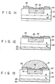
- Figs. 7-13 collectively show how to produce the semiconductor device shown in Fig. 6.
- insulation films 24, 25 are formed by thermal oxidation on the surfaces of a semiconductor substrate 20 comprising an N-type semiconductor region 21 and an N +- type semiconductor region 22, as shown in Fig. 7.
- the insulation film 25 on the back surface of the substrate 20 is removed, while the insulation film 24 on the front surface is selectively removed by etching so as to provide an opening.
- a P-type impurity is diffused through the opening into the substrate to form a P *- type region 25 of a prescribed depth, followed by forming a thin insulation film 26 to cover the remaining insulation film 24 and the exposed surface of the P I- type region 25, as shown in Fig. 8.
- a front surface electrode is formed before polishing the back side of the substrate 20.
- the thin insulation film 26 on the front surface is patterned to provide an opening 27 as shown in Fig. 9, followed by forming a front surface electrode 28 connected to the P +- type region 25 as shown in Fig. 10.
- the front surface electrode 28 is formed by vapor deposition of a gold alloy, e.g., a Au-Ga alloy, followed by selective etching of the deposited alloy layer.
- the back side of the substrate 20 is polished by the ordinary method so as to reduce the thickness of the N +- region 22 to a prescribed extent.
- a thin N +- type region 23 results from the polishing treatment.
- the substrate thickness is reduced from about 350 ⁇ m to about 180 ⁇ m by the polishing treatment.
- the substrate thinned by the polishing treatment has lower mechanical strength.
- a masking step in which load is applied to the substrate, is not employed later because the front surface electrode is formed in advance.
- the substrate is not exposed to high temperatures as described previously. It follows that it is possible to substantially prevent the substrate from being cracked or broken in the manufacturing process of the semiconductor device.
- the insulation films are selectively etched before the polishing step. Thus, the insulation films are free from pin holes caused by the debris accompanying the polishing step.
- a back surface electrode consisting of a gold alloy layer 29 having a thickness of, for example, 1000-2000 A and a silver layer 30 having a thickness of 1.5-3.0 pm are formed by vapor deposition on the thin N *- type region 23, as shown in Fig. 12.
- the gold alloy layer 29 consists mainly of a Au-Ge alloy.
- a silver bumper 31 is formed on the front surface electrode 28 by the method described previously so as to produce a desired semiconductor device, shown in Fig. 13.
- the polishing treatment of the back side of the substrate is performed in the present invention after formation of the front surface electrode.
- the heat treatment at temperatures of about 700°C which is required in the prior art, need not be employed in the present invention.
- the insulation film-in direct contact with the semiconductor region is selectively etched to form the front surface electrode before the polishing treatment.
Landscapes
- Electrodes Of Semiconductors (AREA)
- Die Bonding (AREA)
Claims (4)
Applications Claiming Priority (2)
| Application Number | Priority Date | Filing Date | Title |
|---|---|---|---|
| JP87033/83 | 1983-05-18 | ||
| JP58087033A JPS59213145A (ja) | 1983-05-18 | 1983-05-18 | 半導体装置及びその製造方法 |
Publications (2)
| Publication Number | Publication Date |
|---|---|
| EP0127089A1 EP0127089A1 (de) | 1984-12-05 |
| EP0127089B1 true EP0127089B1 (de) | 1990-01-31 |
Family
ID=13903635
Family Applications (1)
| Application Number | Title | Priority Date | Filing Date |
|---|---|---|---|
| EP84105669A Expired - Lifetime EP0127089B1 (de) | 1983-05-18 | 1984-05-18 | Halbleiterelement mit zwei Elektroden und Verfahren zu seiner Herstellung |
Country Status (4)
| Country | Link |
|---|---|
| US (1) | US4914054A (de) |
| EP (1) | EP0127089B1 (de) |
| JP (1) | JPS59213145A (de) |
| DE (1) | DE3481249D1 (de) |
Cited By (1)
| Publication number | Priority date | Publication date | Assignee | Title |
|---|---|---|---|---|
| EP2312622B1 (de) * | 2009-10-15 | 2019-10-23 | Mitsubishi Electric Corporation | Leistungshalbleitervorrichtung mit einem Substrat mittels eines Sn-Sb-Cu-Lotes verbundenen Leistungshalbleiterbauelement und mit einem mit dem Substrat mittels eines Sn-Ag-basierten oder Sn-Ag-Cu-basierten Lotes verbundenen Anschlusselement und Herstellungsverfahren dafür |
Families Citing this family (7)
| Publication number | Priority date | Publication date | Assignee | Title |
|---|---|---|---|---|
| US5342793A (en) * | 1990-02-20 | 1994-08-30 | Sgs-Thomson Microelectronics, S.R.L. | Process for obtaining multi-layer metallization of the back of a semiconductor substrate |
| US5252180A (en) * | 1990-05-17 | 1993-10-12 | Xerox Corporation | Electrical contacts for an electro-optic modulator |
| US5404047A (en) * | 1992-07-17 | 1995-04-04 | Lsi Logic Corporation | Semiconductor die having a high density array of composite bond pads |
| US5248903A (en) * | 1992-09-18 | 1993-09-28 | Lsi Logic Corporation | Composite bond pads for semiconductor devices |
| EP0646959B1 (de) * | 1993-09-30 | 2001-08-16 | Consorzio per la Ricerca sulla Microelettronica nel Mezzogiorno | Verfahren zur Metallisierung und Verbindung bei der Herstellung von Leistungshalbleiterbauelementen |
| JPH07307306A (ja) * | 1994-05-10 | 1995-11-21 | Nissan Motor Co Ltd | 半導体装置の製造方法 |
| JP3160205B2 (ja) * | 1996-09-02 | 2001-04-25 | 科学技術振興事業団 | 半導体装置の製造方法およびその製造装置 |
Citations (1)
| Publication number | Priority date | Publication date | Assignee | Title |
|---|---|---|---|---|
| US3434828A (en) * | 1963-02-01 | 1969-03-25 | Texas Instruments Inc | Gold alloy for attaching a lead to a semiconductor body |
Family Cites Families (13)
| Publication number | Priority date | Publication date | Assignee | Title |
|---|---|---|---|---|
| BE575275A (de) * | 1958-02-03 | 1900-01-01 | ||
| US3200490A (en) * | 1962-12-07 | 1965-08-17 | Philco Corp | Method of forming ohmic bonds to a germanium-coated silicon body with eutectic alloyforming materials |
| GB1337283A (en) * | 1969-12-26 | 1973-11-14 | Hitachi Ltd | Method of manufacturing a semiconductor device |
| US4042951A (en) * | 1975-09-25 | 1977-08-16 | Texas Instruments Incorporated | Gold-germanium alloy contacts for a semiconductor device |
| DE2603745C3 (de) * | 1976-01-31 | 1981-07-23 | Licentia Patent-Verwaltungs-Gmbh, 6000 Frankfurt | Mehrschichtiger Metallanschlußkontakt und Verfahren zu seiner Herstellung |
| JPS5441067A (en) * | 1977-09-08 | 1979-03-31 | Nec Home Electronics Ltd | Production of semiconductor devices |
| JPS5685841A (en) * | 1979-12-14 | 1981-07-13 | Hitachi Ltd | Semiconductor element |
| JPS5688340A (en) * | 1979-12-21 | 1981-07-17 | Hitachi Ltd | Heat resistant electrode and manufacture thereof |
| JPS5772351A (en) * | 1980-10-24 | 1982-05-06 | Hitachi Ltd | Fabrication of wiring structure |
| JPS57154844A (en) * | 1981-03-20 | 1982-09-24 | Hitachi Ltd | Semiconductor element |
| US4403397A (en) * | 1981-07-13 | 1983-09-13 | The United States Of America As Represented By The Secretary Of The Navy | Method of making avalanche photodiodes |
| JPS6173326A (ja) * | 1984-09-19 | 1986-04-15 | Hitachi Ltd | 半導体装置の製造方法 |
| JPS61232625A (ja) * | 1985-04-09 | 1986-10-16 | Nec Corp | 半導体装置の製造方法 |
-
1983
- 1983-05-18 JP JP58087033A patent/JPS59213145A/ja active Pending
-
1984
- 1984-05-18 DE DE8484105669T patent/DE3481249D1/de not_active Expired - Lifetime
- 1984-05-18 EP EP84105669A patent/EP0127089B1/de not_active Expired - Lifetime
-
1986
- 1986-10-29 US US06/925,490 patent/US4914054A/en not_active Expired - Lifetime
Patent Citations (1)
| Publication number | Priority date | Publication date | Assignee | Title |
|---|---|---|---|---|
| US3434828A (en) * | 1963-02-01 | 1969-03-25 | Texas Instruments Inc | Gold alloy for attaching a lead to a semiconductor body |
Cited By (1)
| Publication number | Priority date | Publication date | Assignee | Title |
|---|---|---|---|---|
| EP2312622B1 (de) * | 2009-10-15 | 2019-10-23 | Mitsubishi Electric Corporation | Leistungshalbleitervorrichtung mit einem Substrat mittels eines Sn-Sb-Cu-Lotes verbundenen Leistungshalbleiterbauelement und mit einem mit dem Substrat mittels eines Sn-Ag-basierten oder Sn-Ag-Cu-basierten Lotes verbundenen Anschlusselement und Herstellungsverfahren dafür |
Also Published As
| Publication number | Publication date |
|---|---|
| DE3481249D1 (de) | 1990-03-08 |
| EP0127089A1 (de) | 1984-12-05 |
| JPS59213145A (ja) | 1984-12-03 |
| US4914054A (en) | 1990-04-03 |
Similar Documents
| Publication | Publication Date | Title |
|---|---|---|
| US3361592A (en) | Semiconductor device manufacture | |
| US4970571A (en) | Bump and method of manufacturing the same | |
| US3760238A (en) | Fabrication of beam leads | |
| US3632436A (en) | Contact system for semiconductor devices | |
| US4179534A (en) | Gold-tin-gold ohmic contact to N-type group III-V semiconductors | |
| US4543444A (en) | Solar-cell | |
| EP0127089B1 (de) | Halbleiterelement mit zwei Elektroden und Verfahren zu seiner Herstellung | |
| US3212160A (en) | Method of manufacturing semiconductive devices | |
| US4042951A (en) | Gold-germanium alloy contacts for a semiconductor device | |
| US3298093A (en) | Bonding process | |
| US3636617A (en) | Method for fabricating monolithic light-emitting semiconductor diodes and arrays thereof | |
| US4232440A (en) | Contact structure for light emitting device | |
| US3290565A (en) | Glass enclosed, passivated semiconductor with contact means of alternate layers of chromium, silver and chromium | |
| US3698941A (en) | Method of applying contacts to a semiconductor body | |
| US3874072A (en) | Semiconductor structure with bumps and method for making the same | |
| US3266137A (en) | Metal ball connection to crystals | |
| US4187599A (en) | Semiconductor device having a tin metallization system and package containing same | |
| US3636618A (en) | Ohmic contact for semiconductor devices | |
| US3349296A (en) | Electronic semiconductor device | |
| US3324015A (en) | Electroplating process for semiconductor devices | |
| EP0514297B1 (de) | Verfahren zum Herstellen eines Kontakts auf einem Halbleiterbauelement | |
| JP3339549B2 (ja) | ガラス被覆半導体装置及びその製造方法 | |
| US4023258A (en) | Method of manufacturing semiconductor diodes for use in millimeter-wave circuits | |
| JPS647542A (en) | Formation of bump | |
| US4077045A (en) | Metallization system for semiconductive devices, devices utilizing such metallization system and method for making devices and metallization system |
Legal Events
| Date | Code | Title | Description |
|---|---|---|---|
| PUAI | Public reference made under article 153(3) epc to a published international application that has entered the european phase |
Free format text: ORIGINAL CODE: 0009012 |
|
| 17P | Request for examination filed |
Effective date: 19840518 |
|
| AK | Designated contracting states |
Designated state(s): DE FR GB |
|
| 17Q | First examination report despatched |
Effective date: 19860203 |
|
| D17Q | First examination report despatched (deleted) | ||
| GRAA | (expected) grant |
Free format text: ORIGINAL CODE: 0009210 |
|
| AK | Designated contracting states |
Kind code of ref document: B1 Designated state(s): DE FR GB |
|
| REF | Corresponds to: |
Ref document number: 3481249 Country of ref document: DE Date of ref document: 19900308 |
|
| ET | Fr: translation filed | ||
| PLBE | No opposition filed within time limit |
Free format text: ORIGINAL CODE: 0009261 |
|
| STAA | Information on the status of an ep patent application or granted ep patent |
Free format text: STATUS: NO OPPOSITION FILED WITHIN TIME LIMIT |
|
| 26N | No opposition filed | ||
| PGFP | Annual fee paid to national office [announced via postgrant information from national office to epo] |
Ref country code: GB Payment date: 19970509 Year of fee payment: 14 |
|
| PGFP | Annual fee paid to national office [announced via postgrant information from national office to epo] |
Ref country code: FR Payment date: 19970513 Year of fee payment: 14 |
|
| PGFP | Annual fee paid to national office [announced via postgrant information from national office to epo] |
Ref country code: DE Payment date: 19970523 Year of fee payment: 14 |
|
| PG25 | Lapsed in a contracting state [announced via postgrant information from national office to epo] |
Ref country code: GB Free format text: LAPSE BECAUSE OF NON-PAYMENT OF DUE FEES Effective date: 19980518 |
|
| PG25 | Lapsed in a contracting state [announced via postgrant information from national office to epo] |
Ref country code: FR Free format text: LAPSE BECAUSE OF NON-PAYMENT OF DUE FEES Effective date: 19980531 |
|
| GBPC | Gb: european patent ceased through non-payment of renewal fee |
Effective date: 19980518 |
|
| PG25 | Lapsed in a contracting state [announced via postgrant information from national office to epo] |
Ref country code: DE Free format text: LAPSE BECAUSE OF NON-PAYMENT OF DUE FEES Effective date: 19990302 |
|
| REG | Reference to a national code |
Ref country code: FR Ref legal event code: ST |
|
| APAH | Appeal reference modified |
Free format text: ORIGINAL CODE: EPIDOSCREFNO |