EP0127295A1 - Anordnung einer Testprobe für ein IC-Plättchen - Google Patents
Anordnung einer Testprobe für ein IC-Plättchen Download PDFInfo
- Publication number
- EP0127295A1 EP0127295A1 EP84302479A EP84302479A EP0127295A1 EP 0127295 A1 EP0127295 A1 EP 0127295A1 EP 84302479 A EP84302479 A EP 84302479A EP 84302479 A EP84302479 A EP 84302479A EP 0127295 A1 EP0127295 A1 EP 0127295A1
- Authority
- EP
- European Patent Office
- Prior art keywords
- wires
- assembly
- chip
- card
- ring
- Prior art date
- Legal status (The legal status is an assumption and is not a legal conclusion. Google has not performed a legal analysis and makes no representation as to the accuracy of the status listed.)
- Granted
Links
Images

Classifications
-
- G—PHYSICS
- G01—MEASURING; TESTING
- G01R—MEASURING ELECTRIC VARIABLES; MEASURING MAGNETIC VARIABLES
- G01R1/00—Details of instruments or arrangements of the types included in groups G01R5/00 - G01R13/00 and G01R31/00
- G01R1/02—General constructional details
- G01R1/06—Measuring leads; Measuring probes
- G01R1/067—Measuring probes
- G01R1/073—Multiple probes
- G01R1/07307—Multiple probes with individual probe elements, e.g. needles, cantilever beams or bump contacts, fixed in relation to each other, e.g. bed of nails fixture or probe card
- G01R1/07342—Multiple probes with individual probe elements, e.g. needles, cantilever beams or bump contacts, fixed in relation to each other, e.g. bed of nails fixture or probe card the body of the probe being at an angle other than perpendicular to test object, e.g. probe card
Definitions
- This invention relates generally to the testing of integrated circuit chips, and, more particularly to a microelectronic test probe assembly for this purpose.
- the input, output, power supply and other terminals of the circuit are formed by metallized contacts, usually deployed along the margins of the circuit pattern.
- the outline of the chip is either square or rectangular, and the marginal locations of the contacts thereon depend on the circuit configuration and the available marginal space. In some instances, therefore, the contacts may lie in uniform rows along the margins, and in other cases, the contacts may be randomly spaced from each other.
- the probe card For the purpose of testing any type of integrated-circuit patterns, before the application thereto of leads to connect the contacts to other components, various types of test probe cards have been developed.
- the probe card consists of a printed circuit board having an opening or port therein to provide access to an IC pattern. This opening is surrounded by a circle of conductive pads connected by-the traces of the printed circuit to terminals on the card which, in turn, are connected to test equipment appropriate to the circuit. The number of pads in the circle determine the maximum capacity of the probe card. If, for example, the card has forty-eight pads, it is capable of testing IC patterns having forty-eight contacts or less.
- probes constituted by needles of tungsten are affixed to selected pads, the needles extending across the opening.
- the length and orientation of each needle is such that its point is adapted to engage a respective contact on the IC pattern.
- the Garretson et al. patents 3,835,381 and 3,905,098 disclose a structure in which needle-like probes formed of tungsten wire are supported on the tapered face of a dielectric base ring surrounding a circular opening in the card, the wires being in a generally conical array with respect to the opening.
- a layer of dielectric material adherent to the tapered surface of the ring acts to secure the wires thereto, the wires being embedded in the layer.
- the outer ends of the wires are connected to terminals on the card, whereas the inner ends leading to the apex of the cone are bent down to form tips which engage the respective contacts on the IC chip to be tested.
- an epoxy or other dielectric material is superimposed over the array of needle probes so as to embed the probes at their assigned angle and position in the epoxy.
- the assembly so arranged is then heated to cause hardening of the epoxy to thereby retain the array of needles at their selected sites.
- test probe card of the Garretson et al. type it is a relatively difficult matter to construct a test probe card of the Garretson et al. type; for to create the necessary conical array of needles, one must use a jig having a conical configuration; and because the needles must be positioned at various angles relative to the conical surface of the jig, the needles make point contact with the jig only at the back end thereof and tend to fall out of position. Also, it is difficult to set the needles relative to the jig to allow proper clearance therebetween for epoxy flow.
- a further disadvantage is that because the needles are at different angles, the scrub characteristics of the needles are not uniform. Moreover, as needles are added to the jig, it is impossible to control the final angle of each needle, as all needles in the jig have slightly different angles due to the cone effect.
- the main object of this invention is to provide a probe test assembly for testing integrated circuit chips in which a radial array of fine wires, all lying in a horizontal plane, are supported on a mounting ring surrounding a circular port in a card, the wires converging toward the central region of the port below which is exposed the chip to be tested, the leading ends of the wires being double bent to define obtuse angle needles whose tips engage the respective contacts of the chip.
- test probe assembly in accordance with the invention is the uniform and consistent scrubbing of the needle point of contact against the microelectronic device under test.
- Yet another object of the invention is to provide a probe test assembly in which the radial array of wires lies in a horizontal plane, thereby obviating the need for feeler gauges to locate and orient the wires on a probe ring fixture, as in prior art arrangements.
- a test probe assembly for checking an integrated circuit chip before terminal leads are applied to the contacts thereof which are deployed on the chip in a common plane.
- the assembly includes a planar insulation card provided with a port and having a printed circuit thereon whose traces are connected to a plurality of test terminals connectable to external testing equipment.
- a mounting ring of dielectric material Surrounding the port and bonded to the card is a mounting ring of dielectric material having a flat face on which is supported a radial array of fine wires. These are maintained in their assigned positions by a layer of dielectric material adherent to the face, the wires being embedded in the layer.
- the wires cantilever across the port and converge toward the central region thereof, below which is disposed the chip to be tested, the leading ends of the wires being double bent to define obtuse angle needles whose tips engage the respective contacts on the chip.
- the trailing ends of the wire which diverge outwardly from the ring are soldered to the traces whereby each needle is connected to a respective test terminal.
- test probe assembly in accordance with the invention for -checking an integrated circuit chip before leads are connected to the contacts of the chip.
- the function of the test probe assembly is to engage the chip contacts and connect them to test terminals which in turn are connected to external test equipment so that the chip circuits may be fully tested to be sure that it satisfies the specifications therefor before the chip is permanently connected to its associated components.
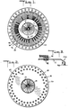
- the assembly includes a planar printed circuit board or card 10 fabricated of synthetic plastic or other insulating material which is structurally stable and of adequate strength.
- Card 10 which in the embodiment illustrated is circular in form, is provided with a circular central opening or port 11 to provide access to the chip to be tested.
- the planar card may be rectangular or in any other suitable configuration; and the port, rather than being circular, may be oblong or in any other geometrical form.
- Traces 13 are conn- .ected to test terminals 14 in an outer circular series thereof adjacent the periphery of the card.
- Traces 12, which are somewhat shorter than traces 13, are connected to test terminals 15 in an inner circular series thereof concentric with the outer series.
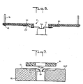
- Each test terminal on the card takes the form of a metal grommet inserted in a card hole and adapted to receive a plug-in pin 16, as shown in Fig. 6, whereby the assembly can be plugged into a test equipment socket rather than being wires thereto terminal by terminal.
- the grommets instead of being discrete elements, may be formed by plating the hole surfaces.
- the terminals may take the form of edge contacts plated on the surface of the card.
- a mounting ring 16 which may be formed of ceramic, anodized aluminium or other dielectric material.
- the ring thus has a flat face parallel to the plane of the card for supporting at a raised position a radial array of fine wires 17, preferably made of tungsten.
- These wires are maintained in their assigned positions by a layer 18 of dielectric material which is adhered to the face of the ring, the wires being embedded therein.
- the layer may be molded of epoxy resin.
- Wires 17 cantilever across port 11 and converge toward the central region 19 thereof, as shown in Fig. 4, just below which is the integrated circuit chip 20 to be tested.
- Chip 20, as shown in Fig. 5, has contacts 21 deployed thereon, all lying in a common horizontal plane, the contacts being located adjacent the margins of the chip.
- each wire is double bent to define an obtuse angle needle 17N.
- the knee angle 0 is such that the tip of the needle which engages a contact on the chip, is at right angles to wire 17, this angle being uniform throughout the array. All needle tips in the array can therefore be viewed identically under the microscope. This improves alignment and placement of the finished test probe assembly when in use for electrical test and measurement. In practice, angle 0 need not be a right angle.
- the number of wires 17 in the array and their placement is determined by the number of contacts 21 and their placement on the integrated circuit chip 20 to be tested.
- the chip illustrated in Fig. 5 there are a relatively small number of contacts 21 deployed on chip 20; hence an equally small number of wires are required in the radial array, the placement of the wires being determined by the placement of these contacts. In practice, a much greater number of contacts and wires may be involved.
- a jig 22 for fabricating a sub-assembly in accordance with the invention the sub-assembly being in the form of a spider-like structure in which a radial array of needles are supported on mounting ring 16 and maintained at their assigned positions by a layer 18 of epoxy material adherent to the face of the ring, the wires being embedded therein.
- Jig 22 is provided with a planar face 22 and a central circular bore 23.
- An annular channel 24 is formed in the jig concentric with bore 23 to receive the flow of the moldable, resinous dielectric material.
- Tungsten wires 17 are laid down on planar face 22P to create the desired radial array, the obtuse angle needles 17N lying within the opening, with the needle tip being received in the separate - apertures of a patterned mask 25.
- This mask is preferably formed of a thin sheet of "Mylar” in a selected pattern determined by the contact position of the chip to be tested.
- Channel 24 is of uniform depth to form the desired thickness of the adhered layer 18.
- These wires may be of tungsten, beryllium- copper or other suitable metal alloys.
- ring 16 whose underside is coated with epoxy, is brought down on the array and clamped to the jig in a fixture.
- This fixture is then placed in an oven and heated to a temperature of about 200°F for a period, such as one hour, sufficient to effect curing and hardening of the resinous layer of dielectric epoxy in which the wires are embedded.
- the resultant spider sub-assembly is removed from the fixture, the ring is bonded to the card around the port therein, and finally the trailing ends of the wires are soldered to the traces of the printed circuit.
Landscapes
- Physics & Mathematics (AREA)
- General Physics & Mathematics (AREA)
- Testing Or Measuring Of Semiconductors Or The Like (AREA)
- Measuring Leads Or Probes (AREA)
Applications Claiming Priority (2)
| Application Number | Priority Date | Filing Date | Title |
|---|---|---|---|
| US49123383A | 1983-05-03 | 1983-05-03 | |
| US491233 | 1983-05-03 |
Publications (2)
| Publication Number | Publication Date |
|---|---|
| EP0127295A1 true EP0127295A1 (de) | 1984-12-05 |
| EP0127295B1 EP0127295B1 (de) | 1987-07-29 |
Family
ID=23951324
Family Applications (1)
| Application Number | Title | Priority Date | Filing Date |
|---|---|---|---|
| EP19840302479 Expired EP0127295B1 (de) | 1983-05-03 | 1984-04-11 | Anordnung einer Testprobe für ein IC-Plättchen |
Country Status (3)
| Country | Link |
|---|---|
| EP (1) | EP0127295B1 (de) |
| JP (1) | JPS59204246A (de) |
| DE (1) | DE3465147D1 (de) |
Cited By (2)
| Publication number | Priority date | Publication date | Assignee | Title |
|---|---|---|---|---|
| FR2571861A1 (fr) * | 1984-10-16 | 1986-04-18 | Radiotechnique Compelec | Tete de mesure pour tester sous pointes des circuits |
| EP0220830A3 (de) * | 1985-09-26 | 1987-10-21 | Tektronix, Inc. | Sondenkopf für Wafer und Verfahren zum Montieren eines Sondenkopfes für Wafer |
Families Citing this family (1)
| Publication number | Priority date | Publication date | Assignee | Title |
|---|---|---|---|---|
| JPS6181237A (ja) * | 1984-09-29 | 1986-04-24 | Aisin Seiki Co Ltd | 車速制御装置 |
Citations (5)
| Publication number | Priority date | Publication date | Assignee | Title |
|---|---|---|---|---|
| US3835381A (en) * | 1969-02-14 | 1974-09-10 | Tieco Inc | Probe card including a multiplicity of probe contacts and methods of making |
| US3891924A (en) * | 1973-09-10 | 1975-06-24 | Probe Rite Inc | Adjustable multi-point probe head assembly |
| US3905098A (en) * | 1973-08-09 | 1975-09-16 | Xynetics Inc | Microelectronic test probe card including a multiplicity of probe contacts and method of making same |
| DE1910314B2 (de) * | 1969-02-28 | 1977-03-17 | Licentia Patent-Verwaltungs-Gmbh, 6000 Frankfurt | Kontaktvorrichtung fuer eine messanordnung zur dynamischen messung von halbleiterparametern |
| US4161692A (en) * | 1977-07-18 | 1979-07-17 | Cerprobe Corporation | Probe device for integrated circuit wafers |
Family Cites Families (3)
| Publication number | Priority date | Publication date | Assignee | Title |
|---|---|---|---|---|
| JPS5375870A (en) * | 1976-12-17 | 1978-07-05 | Hitachi Ltd | Semiconductor device measuring jig |
| JPS5922810B2 (ja) * | 1977-07-19 | 1984-05-29 | カネボウ株式会社 | ポリエステルミシン糸の製造法 |
| JPS5666053A (en) * | 1979-11-01 | 1981-06-04 | Mitsubishi Electric Corp | Fixed probing card |
-
1984
- 1984-04-11 EP EP19840302479 patent/EP0127295B1/de not_active Expired
- 1984-04-11 DE DE8484302479T patent/DE3465147D1/de not_active Expired
- 1984-04-13 JP JP7310084A patent/JPS59204246A/ja active Pending
Patent Citations (5)
| Publication number | Priority date | Publication date | Assignee | Title |
|---|---|---|---|---|
| US3835381A (en) * | 1969-02-14 | 1974-09-10 | Tieco Inc | Probe card including a multiplicity of probe contacts and methods of making |
| DE1910314B2 (de) * | 1969-02-28 | 1977-03-17 | Licentia Patent-Verwaltungs-Gmbh, 6000 Frankfurt | Kontaktvorrichtung fuer eine messanordnung zur dynamischen messung von halbleiterparametern |
| US3905098A (en) * | 1973-08-09 | 1975-09-16 | Xynetics Inc | Microelectronic test probe card including a multiplicity of probe contacts and method of making same |
| US3891924A (en) * | 1973-09-10 | 1975-06-24 | Probe Rite Inc | Adjustable multi-point probe head assembly |
| US4161692A (en) * | 1977-07-18 | 1979-07-17 | Cerprobe Corporation | Probe device for integrated circuit wafers |
Cited By (2)
| Publication number | Priority date | Publication date | Assignee | Title |
|---|---|---|---|---|
| FR2571861A1 (fr) * | 1984-10-16 | 1986-04-18 | Radiotechnique Compelec | Tete de mesure pour tester sous pointes des circuits |
| EP0220830A3 (de) * | 1985-09-26 | 1987-10-21 | Tektronix, Inc. | Sondenkopf für Wafer und Verfahren zum Montieren eines Sondenkopfes für Wafer |
Also Published As
| Publication number | Publication date |
|---|---|
| JPS59204246A (ja) | 1984-11-19 |
| EP0127295B1 (de) | 1987-07-29 |
| DE3465147D1 (en) | 1987-09-03 |
Similar Documents
| Publication | Publication Date | Title |
|---|---|---|
| US4599559A (en) | Test probe assembly for IC chips | |
| US4719417A (en) | Multi-level test probe assembly for IC chips | |
| US4523144A (en) | Complex probe card for testing a semiconductor wafer | |
| US3849728A (en) | Fixed point probe card and an assembly and repair fixture therefor | |
| US3930809A (en) | Assembly fixture for fixed point probe card | |
| US5872459A (en) | Method of testing integrated circuits | |
| US5589781A (en) | Die carrier apparatus | |
| US5629837A (en) | Button contact for surface mounting an IC device to a circuit board | |
| US5521518A (en) | Probe card apparatus | |
| US6037785A (en) | Probe card apparatus | |
| US6137297A (en) | Electronic test probe interface assembly and method of manufacture | |
| US4975638A (en) | Test probe assembly for testing integrated circuit devices | |
| US6861858B2 (en) | Vertical probe card and method for using the same | |
| US4382228A (en) | Probes for fixed point probe cards | |
| US6429671B1 (en) | Electrical test probe card having a removable probe head assembly with alignment features and a method for aligning the probe head assembly to the probe card | |
| JPH07221146A (ja) | 半導体デバイス用非破壊相互接続システム | |
| US4835464A (en) | Decoupling apparatus for use with integrated circuit tester | |
| US4676564A (en) | Access device unit for installed pin grid array | |
| US7898276B2 (en) | Probe card with stacked substrate | |
| EP0298219A2 (de) | Methode und Vorrichtung zum Prüfen von nicht-gekapselten integrierten Schaltkreisen in einem hybriden Schaltkreis | |
| US4488111A (en) | Coupling devices for operations such as testing | |
| US6292005B1 (en) | Probe card for IC testing apparatus | |
| EP0127295B1 (de) | Anordnung einer Testprobe für ein IC-Plättchen | |
| US5175496A (en) | Dual contact beam assembly for an IC test fixture | |
| US6486688B2 (en) | Semiconductor device testing apparatus having a contact sheet and probe for testing high frequency characteristics |
Legal Events
| Date | Code | Title | Description |
|---|---|---|---|
| PUAI | Public reference made under article 153(3) epc to a published international application that has entered the european phase |
Free format text: ORIGINAL CODE: 0009012 |
|
| AK | Designated contracting states |
Designated state(s): CH DE FR GB IT LI NL SE |
|
| 17P | Request for examination filed |
Effective date: 19850530 |
|
| 17Q | First examination report despatched |
Effective date: 19860410 |
|
| ITF | It: translation for a ep patent filed | ||
| GRAA | (expected) grant |
Free format text: ORIGINAL CODE: 0009210 |
|
| AK | Designated contracting states |
Kind code of ref document: B1 Designated state(s): CH DE FR GB IT LI NL SE |
|
| REF | Corresponds to: |
Ref document number: 3465147 Country of ref document: DE Date of ref document: 19870903 |
|
| ET | Fr: translation filed | ||
| PLBE | No opposition filed within time limit |
Free format text: ORIGINAL CODE: 0009261 |
|
| STAA | Information on the status of an ep patent application or granted ep patent |
Free format text: STATUS: NO OPPOSITION FILED WITHIN TIME LIMIT |
|
| 26N | No opposition filed | ||
| PG25 | Lapsed in a contracting state [announced via postgrant information from national office to epo] |
Ref country code: GB Effective date: 19890411 |
|
| PG25 | Lapsed in a contracting state [announced via postgrant information from national office to epo] |
Ref country code: SE Effective date: 19890412 |
|
| PG25 | Lapsed in a contracting state [announced via postgrant information from national office to epo] |
Ref country code: LI Effective date: 19890430 Ref country code: CH Effective date: 19890430 |
|
| PG25 | Lapsed in a contracting state [announced via postgrant information from national office to epo] |
Ref country code: NL Effective date: 19891101 |
|
| GBPC | Gb: european patent ceased through non-payment of renewal fee | ||
| NLV4 | Nl: lapsed or anulled due to non-payment of the annual fee | ||
| PG25 | Lapsed in a contracting state [announced via postgrant information from national office to epo] |
Ref country code: FR Free format text: LAPSE BECAUSE OF NON-PAYMENT OF DUE FEES Effective date: 19891228 |
|
| REG | Reference to a national code |
Ref country code: CH Ref legal event code: PL |
|
| PG25 | Lapsed in a contracting state [announced via postgrant information from national office to epo] |
Ref country code: DE Effective date: 19900103 |
|
| REG | Reference to a national code |
Ref country code: FR Ref legal event code: ST |
|
| EUG | Se: european patent has lapsed |
Ref document number: 84302479.5 Effective date: 19900412 |