EP0128385A2 - Procédé pour fabriquer un dispositif semi-conducteur ayant des électrodes et des interconnexions - Google Patents
Procédé pour fabriquer un dispositif semi-conducteur ayant des électrodes et des interconnexions Download PDFInfo
- Publication number
- EP0128385A2 EP0128385A2 EP84105533A EP84105533A EP0128385A2 EP 0128385 A2 EP0128385 A2 EP 0128385A2 EP 84105533 A EP84105533 A EP 84105533A EP 84105533 A EP84105533 A EP 84105533A EP 0128385 A2 EP0128385 A2 EP 0128385A2
- Authority
- EP
- European Patent Office
- Prior art keywords
- semiconductor device
- producing
- silicon
- electrode
- silicide
- Prior art date
- Legal status (The legal status is an assumption and is not a legal conclusion. Google has not performed a legal analysis and makes no representation as to the accuracy of the status listed.)
- Ceased
Links
Images
Classifications
-
- H—ELECTRICITY
- H10—SEMICONDUCTOR DEVICES; ELECTRIC SOLID-STATE DEVICES NOT OTHERWISE PROVIDED FOR
- H10D—INORGANIC ELECTRIC SEMICONDUCTOR DEVICES
- H10D30/00—Field-effect transistors [FET]
- H10D30/01—Manufacture or treatment
-
- H—ELECTRICITY
- H10—SEMICONDUCTOR DEVICES; ELECTRIC SOLID-STATE DEVICES NOT OTHERWISE PROVIDED FOR
- H10P—GENERIC PROCESSES OR APPARATUS FOR THE MANUFACTURE OR TREATMENT OF DEVICES COVERED BY CLASS H10
- H10P30/00—Ion implantation into wafers, substrates or parts of devices
- H10P30/20—Ion implantation into wafers, substrates or parts of devices into semiconductor materials, e.g. for doping
- H10P30/202—Ion implantation into wafers, substrates or parts of devices into semiconductor materials, e.g. for doping characterised by the semiconductor materials
- H10P30/204—Ion implantation into wafers, substrates or parts of devices into semiconductor materials, e.g. for doping characterised by the semiconductor materials into Group IV semiconductors
-
- H—ELECTRICITY
- H10—SEMICONDUCTOR DEVICES; ELECTRIC SOLID-STATE DEVICES NOT OTHERWISE PROVIDED FOR
- H10D—INORGANIC ELECTRIC SEMICONDUCTOR DEVICES
- H10D30/00—Field-effect transistors [FET]
- H10D30/01—Manufacture or treatment
- H10D30/061—Manufacture or treatment of FETs having Schottky gates
-
- H—ELECTRICITY
- H10—SEMICONDUCTOR DEVICES; ELECTRIC SOLID-STATE DEVICES NOT OTHERWISE PROVIDED FOR
- H10D—INORGANIC ELECTRIC SEMICONDUCTOR DEVICES
- H10D64/00—Electrodes of devices having potential barriers
- H10D64/01—Manufacture or treatment
- H10D64/011—Manufacture or treatment of electrodes ohmically coupled to a semiconductor
-
- H—ELECTRICITY
- H10—SEMICONDUCTOR DEVICES; ELECTRIC SOLID-STATE DEVICES NOT OTHERWISE PROVIDED FOR
- H10D—INORGANIC ELECTRIC SEMICONDUCTOR DEVICES
- H10D64/00—Electrodes of devices having potential barriers
- H10D64/01—Manufacture or treatment
- H10D64/011—Manufacture or treatment of electrodes ohmically coupled to a semiconductor
- H10D64/0111—Manufacture or treatment of electrodes ohmically coupled to a semiconductor to Group IV semiconductors
- H10D64/0112—Manufacture or treatment of electrodes ohmically coupled to a semiconductor to Group IV semiconductors using conductive layers comprising silicides
-
- H—ELECTRICITY
- H10—SEMICONDUCTOR DEVICES; ELECTRIC SOLID-STATE DEVICES NOT OTHERWISE PROVIDED FOR
- H10P—GENERIC PROCESSES OR APPARATUS FOR THE MANUFACTURE OR TREATMENT OF DEVICES COVERED BY CLASS H10
- H10P14/00—Formation of materials, e.g. in the shape of layers or pillars
- H10P14/40—Formation of materials, e.g. in the shape of layers or pillars of conductive or resistive materials
- H10P14/412—Deposition of metallic or metal-silicide materials
-
- H—ELECTRICITY
- H10—SEMICONDUCTOR DEVICES; ELECTRIC SOLID-STATE DEVICES NOT OTHERWISE PROVIDED FOR
- H10P—GENERIC PROCESSES OR APPARATUS FOR THE MANUFACTURE OR TREATMENT OF DEVICES COVERED BY CLASS H10
- H10P30/00—Ion implantation into wafers, substrates or parts of devices
- H10P30/20—Ion implantation into wafers, substrates or parts of devices into semiconductor materials, e.g. for doping
- H10P30/208—Ion implantation into wafers, substrates or parts of devices into semiconductor materials, e.g. for doping of electrically inactive species
-
- H—ELECTRICITY
- H10—SEMICONDUCTOR DEVICES; ELECTRIC SOLID-STATE DEVICES NOT OTHERWISE PROVIDED FOR
- H10P—GENERIC PROCESSES OR APPARATUS FOR THE MANUFACTURE OR TREATMENT OF DEVICES COVERED BY CLASS H10
- H10P30/00—Ion implantation into wafers, substrates or parts of devices
- H10P30/20—Ion implantation into wafers, substrates or parts of devices into semiconductor materials, e.g. for doping
- H10P30/21—Ion implantation into wafers, substrates or parts of devices into semiconductor materials, e.g. for doping of electrically active species
-
- H—ELECTRICITY
- H10—SEMICONDUCTOR DEVICES; ELECTRIC SOLID-STATE DEVICES NOT OTHERWISE PROVIDED FOR
- H10P—GENERIC PROCESSES OR APPARATUS FOR THE MANUFACTURE OR TREATMENT OF DEVICES COVERED BY CLASS H10
- H10P30/00—Ion implantation into wafers, substrates or parts of devices
- H10P30/20—Ion implantation into wafers, substrates or parts of devices into semiconductor materials, e.g. for doping
- H10P30/28—Ion implantation into wafers, substrates or parts of devices into semiconductor materials, e.g. for doping characterised by an annealing step, e.g. for activation of dopants
-
- H—ELECTRICITY
- H10—SEMICONDUCTOR DEVICES; ELECTRIC SOLID-STATE DEVICES NOT OTHERWISE PROVIDED FOR
- H10P—GENERIC PROCESSES OR APPARATUS FOR THE MANUFACTURE OR TREATMENT OF DEVICES COVERED BY CLASS H10
- H10P95/00—Generic processes or apparatus for manufacture or treatments not covered by the other groups of this subclass
- H10P95/90—Thermal treatments, e.g. annealing or sintering
-
- Y—GENERAL TAGGING OF NEW TECHNOLOGICAL DEVELOPMENTS; GENERAL TAGGING OF CROSS-SECTIONAL TECHNOLOGIES SPANNING OVER SEVERAL SECTIONS OF THE IPC; TECHNICAL SUBJECTS COVERED BY FORMER USPC CROSS-REFERENCE ART COLLECTIONS [XRACs] AND DIGESTS
- Y10—TECHNICAL SUBJECTS COVERED BY FORMER USPC
- Y10S—TECHNICAL SUBJECTS COVERED BY FORMER USPC CROSS-REFERENCE ART COLLECTIONS [XRACs] AND DIGESTS
- Y10S148/00—Metal treatment
- Y10S148/14—Schottky barrier contacts
Definitions
- This invention relates generally to a method of producing a semiconductor device, and more particularly to a method of producing a semiconductor device including a thin diffusion layer having low resistance and metallic electrodes as well as wirings that are electrically connected to the diffusion layer.
- an As-doped region in a 1-mega bit dynamic memory is from about 0.1 to 0.2 pm.
- the resistance in the surface direction of a 0.1 pm-thick impurity-doped region is about 100 ⁇ / ⁇ .
- the source-drain resistance of the MIS transistor becomes high while the channel conductance becomes low, so that the high speed operation of the transistor becomes difficult.
- the impurity-doped region is also used as a wiring of the semiconductor device, signal transmission will be retarded if the resistance becomes high as described above, and from this point, too, the high speed operation is impeded.
- the thickness (depth) of the emitter is ever-decreasing and is from 0.1 to 0.2 um at present.
- the high speed operation of the bipolar semiconductor device is impeded. For this reason, it has been strongly desired to decrease the emitter resistance.
- Polycrystalline silicon has been widely used in the past for the gate electrode of the MIS semiconductor device and its wirings. As the integration density has been increased, however, the high resistance of the polycrystalline silicon renders a serious problem for the high speed operation of the device, and the use of tungsten, molybdenum or their silicides for the gate electrode and the wirings has been proposed.
- the gate electrode and the wirings are composed of the polycrystalline silicon, direct contact with a silicon substrate has been used widely in order to accomplish high integration density.
- Connection of the gate electrode of a load transistor to a driving MOS transistor in an E/D-M OS inverter circuit, for example, has been made by direct connection with the silicon substrate.
- the metal and silicon cause heterogeneous reaction at the portion where they are in contact with each other, and hence peel off.
- the gate electrode made of W or Mo is formed or when the wiring made of W or Mo is used, therefore, it is necessary to avoid the direct contact between the metal and silicon, and this renders a critical problem in order to attain high integration density of the device.
- ions of a metal capable to react with silicon and to form a silicide or its alloy are im- plantedinto a desired surface region of a silicon substrate, so that the silicide or silicon alloy layer is interposed between an electrode or wiring and the silicon substrate in order to prevent the peel of the electrode or wiring, and to establish satisfactory connection between the electrode or wiring and the silicon substrate.
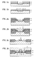
- Figs. 1, 2 and 3 of the accompanying drawings are sectional views of a semiconductor device useful for explaining step-wise the method of producing the semiconductor device in accordance with different embodiments of the present invention.
- An impurity such as P is generally introduced in a dose of about 10 20 /cm 3 into an impurity-doped region. If the reaction between Mo or W and Si occurs as described above, the impurity thus doped migrates into the reaction layer, and the impurity concentration of the impurity-doped region drops to about 10 17 / cm 3 .
- the peel of the electrode and the wiring can be prevented and an ohmic contact can be formed with the silicon substrate when the metal capable of reacting with silicon and forming a silicide or alloy with silicon, such as Mo, W or Ti is ion-implanted into the impurity-doped region on the surface of the silicon substrate, and after the heat-treatment of the substrate to form the silicide or alloy layer, the electrode and wiring made of W, Mo or A l are formed on the resulting silicide or alloy layer.
- the metal capable of reacting with silicon and forming a silicide or alloy with silicon, such as Mo, W or Ti is ion-implanted into the impurity-doped region on the surface of the silicon substrate, and after the heat-treatment of the substrate to form the silicide or alloy layer, the electrode and wiring made of W, Mo or A l are formed on the resulting silicide or alloy layer.
- the silicide or silicon alloy layer is interposed between the electrode or the wiring and the silicon substrate, there is no possibility that the heterogeneous reaction, that would otherwise occur when the electrode and wiring made of W or Mo are directly formed on the silicon substrate, and hence the drop of the impurity concentration in the impurity-doped region resulting from the heterogeneous reaction, occur.
- the formation of the silicide or alloy by heating may be effected after the formation of the electrode and the wiring.
- An extremely excellent Schottky junction can be formed by forming first the silicide or silicon alloy layer on the semiconductor substrate, on which the impurity-doped region is not.yet formed, and then forming an aluminum electrode or the like on the silicide or alloy layer.
- This example illustrates a case in which a W electrode is directly formed on an As-doped region which is formed inside the surface region of a silicon substrate.
- Arsenic ions were selectively implanted into a desired portion of the silicon substrate 1 with the oxide film 6 acting as an ion implantation mask at an acceleration voltage of 80 keV and a dose of 5x10 15 /cm 2 , to form an As-doped region 7.
- the aluminum film 3 at the portion at which a contact aperture was to be formed was selectively removed, and the portion on which the oxide film 6 was exposed was further removed so as to expose the As-doped region 7.
- Tungsten ions were implanted using the aluminum film 3 as the mask at an acceleration voltage of 100 keV and a dose of 5x10 15 /cm 2 to form an implantation region 4.
- the aluminum film 3 was removed using a phosphoric acid type etching solution, followed by heat-treatment at 700°C for 30 minutes.
- a 300 nm-thick W film 5 was then formed by sputtering technology, as shown in Figure lb.
- the unnecessary portions of this W film 5 were selectively removed by reactive sputter etching in a shape of an electrode.
- Heat-treatment was then effected at 1,000°C for 30 minutes.
- the W film 5 thus formed did not at all peel, and the surface of the W film at the portion where it was in.contact with the silicon substrate 1 was flat and smooth.
- the W film was formed without W ion implantation, the W film was likely to peel and even if it did not peel, the surface of the W film became corrugated and a satisfactory W electrode could not be obtained.
- the depth of the As-doped region 7 after heat-treatment was about 0.2 ⁇ m.
- This example illustrates a case in which a satisfactory diode is formed by preventing the reaction between an aluminum electrode and a silicon substrate.
- a 500 nm-thick oxide film 6 for separating devices was formed on a p-type (100) silicon substrate 1 having a resistivity of 10 ⁇ cm, as shown in Figure 2a, and a 20 nm-thick oxide film was formed at the portions other than the oxide film 6.
- Arsenic ions were implanted at an acceleration voltage of 80 k eV and a dose of 5x10 15 /cm 2 to form an n + layer 7..
- a silicate glass film 8 was deposited in a thickness of 500 nm, and the glass film 8 at a desired portion was selectively removed by dry etching to bore a contact hole.
- Tungsten ions were implanted at an acceleration voltage of 100 keV and a dose of 5x10 15 /cm 2 to form an implantation layer 4'.
- the surface layer of the silicate glass film 8 was thinly removed by a hydrofluoric acid type etching solution, and an aluminum electrode 9 was formed by heat-treatment at 950°C for 30 minutes, as shown in Figure 2b.
- silicon was contained in aluminum in order to prevent the occurrence of the alloy pit, but in this example-pure aluminum was used.
- Example 1 As ions and W ionswere implanted in succession to form the n + layer 7 and the ion implantation layer 4. After heat-treatment at 950°C for 30 minutes to form the W silicide layer, the side surface of the As-doped layer 7 was exposed by angle polishing. When the exposed side surface was examined, the n + layer was found formed around the W silicide layer. When this n + layer was observed by an ion microanalyzer, it was found to be a layer containing large quantities of As.
- This example illustrates a case in which the present invention is applied to the production of an MOS transistor having its source and drain formed by Schottky contacts.
- a 500 nm-thick oxide film 6 for separating devices was formed on an n-type (100) silicon substrate 1 having a resistivity of 5 ⁇ cm, as shown in Figure 3a, a 20 nm-thick gate oxide film 2 was formed.
- P-doped polycrystalline silicon was deposited, and unnecessary portions were removed by reactive sputter etching to form a 1 pm-wide gate electrode 10.
- the thin oxide film 2 around the gate electrode 10 was removed by a.hydrofluoric acid type etching solution, and W ions were implanted at 100 keV and a dose of 5x10 15 /cm 2 to form an implantation layer 4".
- those metals which can form silicides or alloys with silicon upon heating can be used as the metals whose ions are to be implanted, and examples of such metals are W, Mo, Al Ti, Ta, and the like.
- the dose of ion implantation of these metals varies depending upon the kind of the metal and upon the kind of the material into which the ions are to be implanted,but the peel of t1 electrode and the wiring can be effectively prevented if the dose is at least about 5x10 14 /cm 2 . If the dose is at least about 5x10¹⁶/cm2, the resistance of the impurity-doped region can be kept at a sufficiently low value in addition to the prevention of the peel of the electrode and the wiring. Hence, such a dose is preferred,particularly,when the depth of the impurity-doped region is small.
- the upper limit of the dose is determined mainly by the limitation to the production process such as the ion implantation time, and the upper limit is substantially about 1x10¹⁸/cm2. If an ion implantation apparatus having higher efficiency is developed or other conditions for the ion implantation are improved, however, the dose may be above 1x10 18 /cm 2 .
- a preferred result can be obtained if the acceleration voltage for the ion implantation is from about 40 to about 150 keV.
- the heat-treating temperature for forming the silicide or alloy with silicon varies depending upon the kind of the metal whose ions are implanted.
- W and Mo for example, their silicides can be formed if they are heated to at least 600°C and to at least 400°C, respectively.
- the silicide or silicon alloy can be formed at a temperature by about 100 to about 150°C lower than the heat-treating temperature of the conventional method which effects heat-treatment after forming the metallic film on silicon, irrespective of the kind of metals. Accordingly, the method of the present invention is by far easier than the conventional method.
- the present invention can effectively prevent the peel of the electrode and the wiring made of a metal, so that these metallic electrode and wiring can be directly formed on the silicon substrate.
- the resistance of the impurity-doped region can be kept as low as from about 20 -to about 50 ⁇ / ⁇ even if the depth of the impurity-doped region is as small as from about 0.1 to about 0.2 ⁇ m.
- the present invention is extremely effective for increasing the integration density and operation speed of LSI/MOS devices and provides the effect of speeding up the access time of a static memory using complementary MOS (C-MOS) transistors.
- C-MOS complementary MOS
- the break-down of the junction can be prevented by the silicide or silicon alloy layer, so that the depth of the impurity-doped region can be extremely reduced.
- the present invention is particularly effective to miniaturize semiconductor devices and to increase their integration density.
- Ai is used for the wiring and the electrode, they can be directly formed on the silicon substrate without the necessity of an intermediate layer, so that the present invention is extremely effective for the production of semiconductor devices.
- W is used for the ion-implantation, but it has been confirmed that the metals usable for the ion-implantation process accord- in g to the present invention are those which form silicides or silicon alloysupon heating, such as Mo, Ta, Ti, Ai, and the like, besides W.
Landscapes
- Electrodes Of Semiconductors (AREA)
- Internal Circuitry In Semiconductor Integrated Circuit Devices (AREA)
Applications Claiming Priority (2)
| Application Number | Priority Date | Filing Date | Title |
|---|---|---|---|
| JP58084221A JPS59210642A (ja) | 1983-05-16 | 1983-05-16 | 半導体装置の製造方法 |
| JP84221/83 | 1983-05-16 |
Publications (2)
| Publication Number | Publication Date |
|---|---|
| EP0128385A2 true EP0128385A2 (fr) | 1984-12-19 |
| EP0128385A3 EP0128385A3 (fr) | 1987-05-13 |
Family
ID=13824423
Family Applications (1)
| Application Number | Title | Priority Date | Filing Date |
|---|---|---|---|
| EP84105533A Ceased EP0128385A3 (fr) | 1983-05-16 | 1984-05-15 | Procédé pour fabriquer un dispositif semi-conducteur ayant des électrodes et des interconnexions |
Country Status (5)
| Country | Link |
|---|---|
| US (1) | US4577396A (fr) |
| EP (1) | EP0128385A3 (fr) |
| JP (1) | JPS59210642A (fr) |
| KR (1) | KR910009783B1 (fr) |
| CA (1) | CA1199430A (fr) |
Cited By (5)
| Publication number | Priority date | Publication date | Assignee | Title |
|---|---|---|---|---|
| EP0259616A1 (fr) * | 1986-09-12 | 1988-03-16 | International Business Machines Corporation | Composant semi-conducteur en silicium et son procédé de fabrication |
| EP0259282A3 (fr) * | 1986-08-29 | 1988-06-08 | Stiftelsen Institutet För Mikrovägsteknik Vid Tekniska Högskolan I Stockholm | Méthode de production de minces couches conductrices et semi-conductrices dans du silicium monocristallin |
| EP0271232A1 (fr) * | 1986-11-24 | 1988-06-15 | AT&T Corp. | Méthode de fabrication d'un article comprenant une structure hétéro-épitaxiale |
| US4894350A (en) * | 1987-09-23 | 1990-01-16 | Siemens Aktiengesellschaft | Method for manufacturing ohmic contacts having low transfer resistances |
| EP0508679A1 (fr) * | 1991-04-11 | 1992-10-14 | AT&T Corp. | Méthode de formation d'une couche de silicide par implantation ionique et composant semiconducteur ainsi produit |
Families Citing this family (17)
| Publication number | Priority date | Publication date | Assignee | Title |
|---|---|---|---|---|
| JPS6063926A (ja) * | 1983-08-31 | 1985-04-12 | Fujitsu Ltd | 半導体装置の製造方法 |
| JPH065750B2 (ja) * | 1985-05-21 | 1994-01-19 | 株式会社日立製作所 | 半導体装置の製造方法 |
| CA1216962A (fr) * | 1985-06-28 | 1987-01-20 | Hussein M. Naguib | Methode de fabrication de dispositifs mos |
| US4742017A (en) * | 1986-06-20 | 1988-05-03 | Ford Aerospace Corporation | Implantation method for forming Schottky barrier photodiodes |
| US5027166A (en) * | 1987-12-04 | 1991-06-25 | Sanken Electric Co., Ltd. | High voltage, high speed Schottky semiconductor device and method of fabrication |
| JPH02170528A (ja) * | 1988-12-23 | 1990-07-02 | Toshiba Corp | 半導体装置の製造方法 |
| US4908334A (en) * | 1989-01-24 | 1990-03-13 | The United States Of America As Represented By The United States Department Of Energy | Method for forming metallic silicide films on silicon substrates by ion beam deposition |
| US5288666A (en) * | 1990-03-21 | 1994-02-22 | Ncr Corporation | Process for forming self-aligned titanium silicide by heating in an oxygen rich environment |
| JPH0680638B2 (ja) * | 1990-07-05 | 1994-10-12 | 株式会社東芝 | 半導体装置の製造方法 |
| US5236872A (en) * | 1991-03-21 | 1993-08-17 | U.S. Philips Corp. | Method of manufacturing a semiconductor device having a semiconductor body with a buried silicide layer |
| US5885896A (en) * | 1996-07-08 | 1999-03-23 | Micron Technology, Inc. | Using implants to lower anneal temperatures |
| JP3199015B2 (ja) * | 1998-02-04 | 2001-08-13 | 日本電気株式会社 | 半導体装置及びその製造方法 |
| DE19853023A1 (de) * | 1998-11-18 | 2000-05-31 | Forschungszentrum Juelich Gmbh | Verfahren zur Herstellung von Nanostrukturen in dünnen Filmen |
| US6562718B1 (en) * | 2000-12-06 | 2003-05-13 | Advanced Micro Devices, Inc. | Process for forming fully silicided gates |
| TW480643B (en) * | 2001-03-20 | 2002-03-21 | Mosel Vitelic Inc | Method for detecting metal on silicon chip by implantation of arsenic ions |
| US6440806B1 (en) * | 2001-04-30 | 2002-08-27 | Advanced Micro Devices, Inc. | Method for producing metal-semiconductor compound regions on semiconductor devices |
| FR2864336B1 (fr) * | 2003-12-23 | 2006-04-28 | Commissariat Energie Atomique | Procede de scellement de deux plaques avec formation d'un contact ohmique entre celles-ci |
Family Cites Families (11)
| Publication number | Priority date | Publication date | Assignee | Title |
|---|---|---|---|---|
| US3600797A (en) * | 1967-12-26 | 1971-08-24 | Hughes Aircraft Co | Method of making ohmic contacts to semiconductor bodies by indirect ion implantation |
| US3560809A (en) * | 1968-03-04 | 1971-02-02 | Hitachi Ltd | Variable capacitance rectifying junction diode |
| US4096622A (en) * | 1975-07-31 | 1978-06-27 | General Motors Corporation | Ion implanted Schottky barrier diode |
| US4206540A (en) * | 1978-06-02 | 1980-06-10 | International Rectifier Corporation | Schottky device and method of manufacture using palladium and platinum intermetallic alloys and titanium barrier |
| US4319395A (en) * | 1979-06-28 | 1982-03-16 | Motorola, Inc. | Method of making self-aligned device |
| JPS5669844A (en) * | 1979-11-10 | 1981-06-11 | Toshiba Corp | Manufacture of semiconductor device |
| US4343082A (en) * | 1980-04-17 | 1982-08-10 | Bell Telephone Laboratories, Incorporated | Method of making contact electrodes to silicon gate, and source and drain regions, of a semiconductor device |
| FR2481005A1 (fr) * | 1980-04-17 | 1981-10-23 | Western Electric Co | Procede de fabrication de transistors a effet de champ a canal court |
| US4339869A (en) * | 1980-09-15 | 1982-07-20 | General Electric Company | Method of making low resistance contacts in semiconductor devices by ion induced silicides |
| JPS584924A (ja) * | 1981-07-01 | 1983-01-12 | Hitachi Ltd | 半導体装置の電極形成方法 |
| US4389257A (en) * | 1981-07-30 | 1983-06-21 | International Business Machines Corporation | Fabrication method for high conductivity, void-free polysilicon-silicide integrated circuit electrodes |
-
1983
- 1983-05-16 JP JP58084221A patent/JPS59210642A/ja active Pending
-
1984
- 1984-04-30 KR KR1019840002313A patent/KR910009783B1/ko not_active Expired
- 1984-05-08 CA CA000453795A patent/CA1199430A/fr not_active Expired
- 1984-05-15 US US06/610,485 patent/US4577396A/en not_active Expired - Fee Related
- 1984-05-15 EP EP84105533A patent/EP0128385A3/fr not_active Ceased
Cited By (5)
| Publication number | Priority date | Publication date | Assignee | Title |
|---|---|---|---|---|
| EP0259282A3 (fr) * | 1986-08-29 | 1988-06-08 | Stiftelsen Institutet För Mikrovägsteknik Vid Tekniska Högskolan I Stockholm | Méthode de production de minces couches conductrices et semi-conductrices dans du silicium monocristallin |
| EP0259616A1 (fr) * | 1986-09-12 | 1988-03-16 | International Business Machines Corporation | Composant semi-conducteur en silicium et son procédé de fabrication |
| EP0271232A1 (fr) * | 1986-11-24 | 1988-06-15 | AT&T Corp. | Méthode de fabrication d'un article comprenant une structure hétéro-épitaxiale |
| US4894350A (en) * | 1987-09-23 | 1990-01-16 | Siemens Aktiengesellschaft | Method for manufacturing ohmic contacts having low transfer resistances |
| EP0508679A1 (fr) * | 1991-04-11 | 1992-10-14 | AT&T Corp. | Méthode de formation d'une couche de silicide par implantation ionique et composant semiconducteur ainsi produit |
Also Published As
| Publication number | Publication date |
|---|---|
| JPS59210642A (ja) | 1984-11-29 |
| CA1199430A (fr) | 1986-01-14 |
| EP0128385A3 (fr) | 1987-05-13 |
| KR840009181A (ko) | 1984-12-21 |
| KR910009783B1 (ko) | 1991-11-30 |
| US4577396A (en) | 1986-03-25 |
Similar Documents
| Publication | Publication Date | Title |
|---|---|---|
| US4577396A (en) | Method of forming electrical contact to a semiconductor substrate via a metallic silicide or silicon alloy layer formed in the substrate | |
| EP0110211B1 (fr) | Circuit intégré à transistors bipolaires et procédé de fabrication de celui-ci | |
| US4551908A (en) | Process of forming electrodes and interconnections on silicon semiconductor devices | |
| US4954855A (en) | Thin film transistor formed on insulating substrate | |
| US4855798A (en) | Semiconductor and process of fabrication thereof | |
| US5103272A (en) | Semiconductor device and a method for manufacturing the same | |
| JP3644983B2 (ja) | 半導体装置の低抵抗接触構造およびその形成方法 | |
| US4107835A (en) | Fabrication of semiconductive devices | |
| US4672419A (en) | Metal gate, interconnect and contact system for VLSI devices | |
| NL8203350A (nl) | Kobaltsilicidemetallisatie voor halfgeleidertransistoren. | |
| US5204276A (en) | Method of manufacturing semiconductor device | |
| US5278099A (en) | Method for manufacturing a semiconductor device having wiring electrodes | |
| EP0051500B1 (fr) | Dispositif semi-conducteur | |
| US4997785A (en) | Shared gate CMOS transistor | |
| EP0338251A1 (fr) | Procédé de fabrication de transistors à effet de champ metal semiconducteur | |
| US4985746A (en) | Semiconductor device and method of production | |
| EP0390509B1 (fr) | Elément semi-conducteur et procédé pour sa réalisation | |
| US4425379A (en) | Polycrystalline silicon Schottky diode array | |
| US5291058A (en) | Semiconductor device silicon via fill formed in multiple dielectric layers | |
| EP0404372B1 (fr) | Procédé pour la fabrication de contacts en silicium polycristallin | |
| EP0093971A2 (fr) | Dispositif semi-conducteur comprenant une couche intermédiaire d'un élément de transition et procédé pour le fabriquer | |
| US5264721A (en) | Insulated-gate FET on an SOI-structure | |
| US6706583B1 (en) | High speed low noise transistor | |
| US4628339A (en) | Polycrystalline silicon Schottky diode array | |
| US5521416A (en) | Semiconductor device having gate electrode and impurity diffusion layer different in conductivity type and method of manufacturing the same |
Legal Events
| Date | Code | Title | Description |
|---|---|---|---|
| PUAI | Public reference made under article 153(3) epc to a published international application that has entered the european phase |
Free format text: ORIGINAL CODE: 0009012 |
|
| AK | Designated contracting states |
Designated state(s): DE FR GB NL |
|
| 17P | Request for examination filed |
Effective date: 19841220 |
|
| PUAL | Search report despatched |
Free format text: ORIGINAL CODE: 0009013 |
|
| AK | Designated contracting states |
Kind code of ref document: A3 Designated state(s): DE FR GB NL |
|
| 17Q | First examination report despatched |
Effective date: 19890502 |
|
| STAA | Information on the status of an ep patent application or granted ep patent |
Free format text: STATUS: THE APPLICATION HAS BEEN REFUSED |
|
| 18R | Application refused |
Effective date: 19910207 |
|
| RIN1 | Information on inventor provided before grant (corrected) |
Inventor name: NAOKI, YAMAMOTO Inventor name: NORIYUKI, SAKUDO |