EP0128559B1 - Gewichtsmessgerät vom Messzellentyp und Methode zur Kontrolle der Empfindlichkeit - Google Patents
Gewichtsmessgerät vom Messzellentyp und Methode zur Kontrolle der Empfindlichkeit Download PDFInfo
- Publication number
- EP0128559B1 EP0128559B1 EP84106584A EP84106584A EP0128559B1 EP 0128559 B1 EP0128559 B1 EP 0128559B1 EP 84106584 A EP84106584 A EP 84106584A EP 84106584 A EP84106584 A EP 84106584A EP 0128559 B1 EP0128559 B1 EP 0128559B1
- Authority
- EP
- European Patent Office
- Prior art keywords
- load cell
- voltage
- amplifier
- output voltage
- measuring device
- Prior art date
- Legal status (The legal status is an assumption and is not a legal conclusion. Google has not performed a legal analysis and makes no representation as to the accuracy of the status listed.)
- Expired
Links
- 230000035945 sensitivity Effects 0.000 title claims description 36
- 238000000034 method Methods 0.000 title claims description 5
- 238000005259 measurement Methods 0.000 claims description 7
- 230000009977 dual effect Effects 0.000 claims description 3
- 230000002401 inhibitory effect Effects 0.000 claims 1
- 238000010586 diagram Methods 0.000 description 4
- 230000004044 response Effects 0.000 description 4
- 239000003990 capacitor Substances 0.000 description 3
- 230000006870 function Effects 0.000 description 3
- 230000003321 amplification Effects 0.000 description 1
- 238000003199 nucleic acid amplification method Methods 0.000 description 1
Images


Classifications
-
- G—PHYSICS
- G01—MEASURING; TESTING
- G01G—WEIGHING
- G01G23/00—Auxiliary devices for weighing apparatus
- G01G23/01—Testing or calibrating of weighing apparatus
-
- G—PHYSICS
- G01—MEASURING; TESTING
- G01G—WEIGHING
- G01G3/00—Weighing apparatus characterised by the use of elastically-deformable members, e.g. spring balances
- G01G3/12—Weighing apparatus characterised by the use of elastically-deformable members, e.g. spring balances wherein the weighing element is in the form of a solid body stressed by pressure or tension during weighing
- G01G3/14—Weighing apparatus characterised by the use of elastically-deformable members, e.g. spring balances wherein the weighing element is in the form of a solid body stressed by pressure or tension during weighing measuring variations of electrical resistance
- G01G3/142—Circuits specially adapted therefor
- G01G3/147—Circuits specially adapted therefor involving digital counting
Definitions
- the present invention relates to a load cell type weight measuring device and a sensitivity checking method thereof.
- Another object of the invention is to provide a sensitivity checking method in the load cell type weight measuring device.
- a load cell type weight measuring device viz. a sensitivity checking method for a load cell type weight measuring device according to claim 8.
- the rated voltage generating circuit and reference potential terminal are coupled with the amplifier circuit at different timings by the switching circuit, and the sensitivity of this load cell type weight measuring device can be easily checked on the basis of the digital data derived at this time from the analog/digital converter.
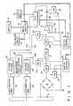
- Fig. 1 shows a circuit of a load cell type weight measuring device according to one embodiment of the present invention.
- This load cell type weight measuring device includes a load cell 2 which is constituted by connecting four strain gauge resistors in a bridge form; a driving power source E for supplying a driving voltage VE to the load cell 2; a low pass filter 4 for removing the AC component from an output signal of the load cell 2; and an amplifier circuit 6 for amplifying an output signal of the low pass filter 4.
- the amplifier circuit 6 includes an operation amplifier 6-1; and resistors R1 and R2 which are connected in series between an output terminal of the amplifier 6-1 and the ground, a junction between these resistors being coupled to an inverting input terminal of the amplifier 6-1.
- An output terminal of the amplifier 6 is coupled to an analog/digital converter 8 through a resistor R3 and a capacitor C1.
- the A/D converter 8 is, for example, of the dual slope type and supplies to a microcomputer 12 a digital data NR corresponding to a difference between an input voltage VI and a reference voltage VR in response to an output pulse from a clock generator 10 for generating a clock pulse of a frequency f e .
- a keyboard circuit 14 which includes a sensitivity checking key and various function keys (not shown) and a display 16 are coupled to the microcomputer 12.
- Both ends of the driving power source E are coupled to respective input terminals of differential amplifier circuits 20 and 22.
- Output terminals of the differential amplifier circuits 20 and 22 are coupled to voltage dividers 24 and 26, respectively.
- the voltage divider 24 divides an output voltage of the differential amplifier circuit 20 and supplies the reference voltage VR to the A/D converter 8.
- a reference point setting circuit 28 divides the output voltage VR of the voltage divider 24 and generates an output voltage VO to set a reference operation point of the A/D converter 8.
- the voltage divider 26 divides an output voltage of the differential amplifier circuit 22 and supplies to the filter 4 a dummy rated voltage VM which is set equal to a rated output voltage generated from the load cell 2 when a rated weight is applied to the load cell 2.
- this load cell type weight measuring device includes switch control circuits 30 and 32; analog switches S1 to S3 which are controlled in response to control signals from the switch control circuit 30; and analog switches S4 to S6 which are controlled in response to control signals from the switch control circuit 32.
- the switch S1 is connected between the output terminal of the load cell 2 and the input terminal of the filter 4.
- the switch S2 is connected between the input terminal of the filter 4 and the ground.
- the switch S3 is connected between an output terminal of the voltage divider 26 and the input terminal of the filter 4.
- the switch S4 is connected between the output terminal of the filter 4 and a noninverting input terminal of the operation amplifier 6-1.
- the switch S5 is connected between an output terminal of the reference point setting circuit 28 and the non-inverting input terminal of the operation amplifier 6-1.
- the switch S6 is connected between the input terminal of the A/D converter 8 and the ground.
- Fig. 2 shows a circuit of the differential amplifier circuits 20 and 22, the voltage dividers 24 and 26, and the reference point setting circuit 28.
- the differential amplifier circuit 20 includes buffer amplifiers 20-1 and 20-2 whose input terminals are respectively coupled to positive and negative terminals of the driving power source E; and a differential amplifier 20-3 whose inverting input terminal and non-inverting input terminal are respectively coupled to output terminals of the buffer amplifiers 20-1 and 20-2 through resistors R4 and R5. An output terminal of the differential amplifier 20-3 is connected through a resistor R6 to its inverting input terminal, while its non-inverting input terminal is grounded through a resistor R7.
- the differential amplifier circuit 22 includes buffer amplifiers 22-1 and 22-2, a differential amplifier 22-3, and resistors R8 to R11 which are connected in the same manner as the buffer amplifiers 20-1 and 20-2, differential amplifier 20-3 and resistors R4 to R7 of the differential amplifier circuit 20.
- the voltage divider 24 includes a resistor R12, a potentiometer RP1 and a resistor R13 which are connected in series between the output terminal of the differential amplifier 20-3 and the ground.
- a wiper terminal of the potentiometer RP1 is coupled to the A/D converter 8.
- the voltage divider 26 includes a resistor R14, a potentiometer RP2 and a resistor R15 which are connected in series between an output terminal of the differential amplifier 22-3 and the ground.
- a wiper terminal of the potentiometer RP2 is connected to the input terminal of the filter 4 through the switch S3.
- the reference point setting circuit 28 includes a buffer amplifier 28-1 whose input terminal is connected to the wiper terminal of the potentiometer RP1, and a resistor R16, a potentiometer RP3 and a resistor R17 which are connected in series between an output terminal of the buffer amplifier 28-1 and the ground.
- a wiper terminal of the potentiometer RP3 is connected to the non-inverting input terminal of the operation amplifier 6-1 through the switch S5.
- an output voltage V28 of the reference point setting circuit 28 is given by the following equation
- the voltage dividing ratio k3 of the voltage divider 26 is determined so as to allow the output voltage V26 of the voltage divider 26 to be equal to the voltage V2 (N).
- a phase setting pulse signal as shown in Fig. 3A is generated in response to a clock pulse from, e.g., the clock generator 10.
- a control signal responsive to this phase setting pulse signal is supplied to the switch control circuit 32 and switch control signals shown in Figs. 3B and 3C are respectively supplied from this switch control 32 to the switch S4 and the switches S5 and S6.
- One cycle of this A/D converting operation is constituted by an offset correction phase P1, an input signal integrating phase P2 and a reference signal integrating phase P3.
- the switch S4 is set into the OFF state and the switches S5 and S6 are set into the ON state, so that the output voltage V28 of the reference point setting circuit 28 is supplied to the operation amplifier 6-1.
- an output voltage V6 (T1) of the amplifier circuit 6 will be given by the following equation.
- the digital output NR of the A/D converter 8 is given by the following equation.
- This equation (12) is implemented by reducing the input voltage V8 at a predetermined rate and counting the time until it reaches the reference level in the reference signal integrating phase P3.
- the interval of this reference signal integrating phase P3 is set into 2T1.
- the microcomputer 12 gives a control signal to the switch control 30, thereby allowing this switch control 30 to supply switch control signals shown in Figs. 5A to 5C to the switches S1 to S3.
- intervals TF1 to TF13 in Figs. 5A to 5C are each equal to the interval of one operation cycle shown in Fig. 3A, and the offset correction phase P1, input signal integrating phase P2 and reference signal integrating phase P3 are included in each interval.
- Figs. 5A to 5C when the weight measuring operation is executed for the intervals T1 and T2 and the sensitivity checking key is operated, the sensitivity checking examination is executed in the intervals TF3 to TF8. Namely, when the switch control signal shown in Fig. 5A is at a high level, the weight measuring mode is set and when the switch control signal of Fig. 5A is at a low level and when the switch S1 is closed, the sensitivity checking mode is set.
- a sensitivity data NRSP can be obtained from the difference between the digital output NR (S2) from the A/D converter 8 which is derived when the switch control signal of Fig. 5B is at a high level to keep the switch S2 ON and the digital output NR (S3) which is derived when the switch control signal of Fig. 5C is at a high level to keep the switch S3 ON.
- the switch S2 is closed in the interval TF3, so that the input voltage of OV is supplied through the filter 4 and switch S4 to the amplifier circuit 6 in the input signal integrating phase P2 and reference signal integrating phase P3.
- This digital output NR (S2) is stored in a memory (not shown) in the microcomputer 12.
- the similar operation is executed, for example, even in the subsequent intervals T4 and T5 and the digital data derived in the respective intervals T3 to T5 are checked to see if they are stable or not.
- the output voltage of the voltage divider 26 is supplied to the amplifier circuit 6 through the filter 4 and switch S4.
- the digital output data NR (S3) from the A/D converter 8 will be given by the following equation.
- This digital output data NR (S3) is also stored in the memory in the microcomputer 12.
- the digital data derived in the intervals TF6, TF7 and TF8 in this way are checked to see if they are stable or not. After they were confirmed to be stable, the sensitivity calculation is immediately executed.
- the microcomputer 12 calculates the difference between the digital output data NR (S2) and NR (S3) stored in the memory to obtain the sensitivity data NRSP represented by the following equation.
- This sensitivity data NRSP is compared with a sensitivity reference value NRRF which has been preset by the microcomputer 12.
- a sensitivity reference value NRRF which has been preset by the microcomputer 12.
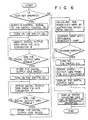
- Fig. 6 shows the flowchart to explain the operation of the load cell type weight measuring device shown in Figs. 1 and 2.
- the microcomputer 12 When it is detected that the sensitivity checking key was operated, the microcomputer 12 first turns on the switch S2 to execute the sensitivity checking examination and turns off the switches S1 and S3. In this state, the digital output data NR (S2) is generated from the A/D converter 8 as indicated in equation (16). In this embodiment, the digital output data are respectively derived in three operation cycles (e.g., intervals TF3, TF4 and TF5). In the case where the maximum error among these three digital output data is less than a predetermined value, one of the three digital output data is stored in the memory as the effective data NR (S2). Then, the switches S1 and S2 are turned off and the switch S3 is turned on.
- the switch S1 and S2 are turned off and the switch S3 is turned on.
- the digital output data NR (S3) is generated from the A/D converter 8 as indicated by equation (17). Also, in this case, the digital output data are respectively derived in three operation cycles (e.g., intervals TF6 to TF8). In the case where the maximum error among these three digital output data is less than a predetermined value, one of the three digital output data is stored in the memory as the effective data NR (S3). Subsequently, the sensitivity NRSP is calculated by subtracting the digital output data NR (S2) from the digital output data NR (S3). The difference between this sensitivity NRSP and the reference sensitivity NRRF is obtained and this difference is checked to see if it is within the permissible range ⁇ a or not.
- the switches S2 and S3 are turned off and the switch S1 is turned on, thereby executing the weight measuring operation.
- the weight measurement data obtained from the A/D converter 8 in this way is displayed on the display 16.
- the microcomputer 12 executes the error indication and at the same time it interrupts the weight measuring operation.
- the present invention has been described in the above with respect to one embodiment, the invention is not limited to only this embodiment.
- the A/D converter 8 of the dual slope type has been used, any other type of A/D converter which is ordinarily well known may be also used.
- the sensitivity checking key has been used in the foregoing embodiment, it is possible to omit this sensitivity checking key and to automatically set the sensitivity checking mode and weight measuring mode alternately.
Landscapes
- Physics & Mathematics (AREA)
- General Physics & Mathematics (AREA)
- Measurement Of Force In General (AREA)
Claims (8)
Applications Claiming Priority (4)
| Application Number | Priority Date | Filing Date | Title |
|---|---|---|---|
| JP10348083A JPS59228120A (ja) | 1983-06-09 | 1983-06-09 | ロ−ドセル秤 |
| JP103480/83 | 1983-06-09 | ||
| JP10348183A JPS59228122A (ja) | 1983-06-09 | 1983-06-09 | ロ−ドセル秤の感度試験方法 |
| JP103481/83 | 1983-06-09 |
Publications (3)
| Publication Number | Publication Date |
|---|---|
| EP0128559A2 EP0128559A2 (de) | 1984-12-19 |
| EP0128559A3 EP0128559A3 (en) | 1986-02-05 |
| EP0128559B1 true EP0128559B1 (de) | 1988-09-21 |
Family
ID=26444117
Family Applications (1)
| Application Number | Title | Priority Date | Filing Date |
|---|---|---|---|
| EP84106584A Expired EP0128559B1 (de) | 1983-06-09 | 1984-06-08 | Gewichtsmessgerät vom Messzellentyp und Methode zur Kontrolle der Empfindlichkeit |
Country Status (3)
| Country | Link |
|---|---|
| US (1) | US4580644A (de) |
| EP (1) | EP0128559B1 (de) |
| DE (1) | DE3474210D1 (de) |
Families Citing this family (7)
| Publication number | Priority date | Publication date | Assignee | Title |
|---|---|---|---|---|
| AU563770B2 (en) * | 1983-12-03 | 1987-07-23 | Ishida Koki Seisakusho K.K. | Electronic weigher |
| US4705126A (en) * | 1985-09-24 | 1987-11-10 | Ishida Scales Manufacturing Company, Ltd. | Signal processing circuit and weighing apparatus incorporating same |
| JPH076823B2 (ja) * | 1986-03-25 | 1995-01-30 | 東京電気株式会社 | ロ−ドセル式秤の抵抗調整方法 |
| DE3938777A1 (de) * | 1989-11-23 | 1991-05-29 | Bosch Gmbh Robert | Schaltungsanordnung zur erkennung von signalstoerungen |
| GB2340951B (en) * | 1998-08-20 | 2000-07-12 | Gec Avery Ltd | Weight simulation calibration rig and method |
| US6079122A (en) * | 1998-08-28 | 2000-06-27 | Rajkovich; Thomas Russell | Weighing dryer |
| US6460008B1 (en) * | 2000-07-19 | 2002-10-01 | Ivan E. Hardt | Yield monitoring system for grain harvesting combine |
Family Cites Families (8)
| Publication number | Priority date | Publication date | Assignee | Title |
|---|---|---|---|---|
| US3728626A (en) * | 1971-03-25 | 1973-04-17 | Colt Ind Operating Corp | Electronic measuring system |
| US4158396A (en) * | 1977-04-22 | 1979-06-19 | Tokyo Electric Co., Ltd. | Electronic weight measuring device |
| CH624484A5 (de) * | 1978-07-14 | 1981-07-31 | Terraillon | |
| JPS6034059B2 (ja) * | 1979-05-15 | 1985-08-06 | 東芝テック株式会社 | 電子式重量測定装置 |
| GB2080540B (en) * | 1980-06-21 | 1983-12-21 | Salter & Co Ltd G | Electrical apparatus for weighing animals |
| DE3176484D1 (en) * | 1980-07-17 | 1987-11-19 | Shimadzu Corp | An electronic balance |
| JPS5753145A (en) * | 1980-09-16 | 1982-03-30 | Sony Tektronix Corp | Calibrator for analogue-digital converter |
| US4535854A (en) * | 1982-11-16 | 1985-08-20 | Pennsylvania Scale Company | Calibration method and apparatus for an electronic weight indicator |
-
1984
- 1984-06-01 US US06/616,557 patent/US4580644A/en not_active Expired - Lifetime
- 1984-06-08 DE DE8484106584T patent/DE3474210D1/de not_active Expired
- 1984-06-08 EP EP84106584A patent/EP0128559B1/de not_active Expired
Also Published As
| Publication number | Publication date |
|---|---|
| EP0128559A2 (de) | 1984-12-19 |
| US4580644A (en) | 1986-04-08 |
| EP0128559A3 (en) | 1986-02-05 |
| DE3474210D1 (en) | 1988-10-27 |
Similar Documents
| Publication | Publication Date | Title |
|---|---|---|
| EP0144834B1 (de) | Wägezellengewichtsmesseinrichtung | |
| US4816745A (en) | Method and arrangement for measuring the resistance ratio in a resistance half-bridge | |
| US4294322A (en) | Electronic weight measuring device | |
| EP0128559A2 (de) | Gewichtsmessgerät vom Messzellentyp und Methode zur Kontrolle der Empfindlichkeit | |
| US4149605A (en) | Scale with digital display | |
| EP0100103B1 (de) | Impulsbreitenmodulator und Integrationsschaltung zur Bildung eines analogen Produkts mit einem solchen Impulsbreitenmodulator | |
| EP0303442B1 (de) | Mehrfrequenz Kapazitäts-Sensor | |
| US4404545A (en) | Analog-to-digital converter of the dual slope type | |
| US5119033A (en) | Vernier voltage-to-digital converter with a storage capacitance selectable in magnitude | |
| EP0692160B1 (de) | Temperaturkorrigierter integrierender analog-digital-wandler | |
| US4445111A (en) | Bi-polar electronic signal converters with single polarity accurate reference source | |
| EP0058050A1 (de) | Frequenzmessverfahren | |
| JPH0365513B2 (de) | ||
| RU2003995C1 (ru) | Устройство дл измерени и контрол параметров стабилизаторов напр жени | |
| SU1686314A1 (ru) | Цифровой тензометр | |
| SU690504A1 (ru) | Интегрирующее устройство | |
| JP3495179B2 (ja) | D/aコンバーターの特性の測定方法及びd/aコンバーターの特性の測定ユニット | |
| SU1167625A1 (ru) | Логарифмический преобразователь | |
| SU1118939A1 (ru) | Устройство дл измерени сопротивлени изол ции сети посто нного тока | |
| SU938287A1 (ru) | Вычислительное устройство дл решени уравнений | |
| JP2671343B2 (ja) | 容量測定装置 | |
| SU1231489A1 (ru) | Устройство дл определени параметров динамического звена второго пор дка | |
| RU2017161C1 (ru) | Устройство для измерения электрических параметров | |
| SU1164558A1 (ru) | Цифровой измеритель тензометрических весов | |
| SU1486944A1 (ru) | Устройство для индикации отклонения переменного напряжения |
Legal Events
| Date | Code | Title | Description |
|---|---|---|---|
| PUAI | Public reference made under article 153(3) epc to a published international application that has entered the european phase |
Free format text: ORIGINAL CODE: 0009012 |
|
| AK | Designated contracting states |
Designated state(s): DE GB |
|
| PUAL | Search report despatched |
Free format text: ORIGINAL CODE: 0009013 |
|
| AK | Designated contracting states |
Designated state(s): DE GB |
|
| 17P | Request for examination filed |
Effective date: 19860724 |
|
| 17Q | First examination report despatched |
Effective date: 19870930 |
|
| GRAA | (expected) grant |
Free format text: ORIGINAL CODE: 0009210 |
|
| AK | Designated contracting states |
Kind code of ref document: B1 Designated state(s): DE GB |
|
| REF | Corresponds to: |
Ref document number: 3474210 Country of ref document: DE Date of ref document: 19881027 |
|
| PLBE | No opposition filed within time limit |
Free format text: ORIGINAL CODE: 0009261 |
|
| STAA | Information on the status of an ep patent application or granted ep patent |
Free format text: STATUS: NO OPPOSITION FILED WITHIN TIME LIMIT |
|
| 26N | No opposition filed | ||
| PGFP | Annual fee paid to national office [announced via postgrant information from national office to epo] |
Ref country code: DE Payment date: 20010605 Year of fee payment: 18 |
|
| PGFP | Annual fee paid to national office [announced via postgrant information from national office to epo] |
Ref country code: GB Payment date: 20010606 Year of fee payment: 18 |
|
| REG | Reference to a national code |
Ref country code: GB Ref legal event code: IF02 |
|
| PG25 | Lapsed in a contracting state [announced via postgrant information from national office to epo] |
Ref country code: GB Free format text: LAPSE BECAUSE OF NON-PAYMENT OF DUE FEES Effective date: 20020608 |
|
| PG25 | Lapsed in a contracting state [announced via postgrant information from national office to epo] |
Ref country code: DE Free format text: LAPSE BECAUSE OF NON-PAYMENT OF DUE FEES Effective date: 20030101 |
|
| GBPC | Gb: european patent ceased through non-payment of renewal fee |
Effective date: 20020608 |