EP0130329B1 - Optisches Datenspeichermedium - Google Patents
Optisches Datenspeichermedium Download PDFInfo
- Publication number
- EP0130329B1 EP0130329B1 EP84105545A EP84105545A EP0130329B1 EP 0130329 B1 EP0130329 B1 EP 0130329B1 EP 84105545 A EP84105545 A EP 84105545A EP 84105545 A EP84105545 A EP 84105545A EP 0130329 B1 EP0130329 B1 EP 0130329B1
- Authority
- EP
- European Patent Office
- Prior art keywords
- layer
- thin film
- substrate
- data storage
- film
- Prior art date
- Legal status (The legal status is an assumption and is not a legal conclusion. Google has not performed a legal analysis and makes no representation as to the accuracy of the status listed.)
- Expired
Links
Images

Classifications
-
- G—PHYSICS
- G11—INFORMATION STORAGE
- G11B—INFORMATION STORAGE BASED ON RELATIVE MOVEMENT BETWEEN RECORD CARRIER AND TRANSDUCER
- G11B7/00—Recording or reproducing by optical means, e.g. recording using a thermal beam of optical radiation by modifying optical properties or the physical structure, reproducing using an optical beam at lower power by sensing optical properties; Record carriers therefor
- G11B7/24—Record carriers characterised by shape, structure or physical properties, or by the selection of the material
- G11B7/2403—Layers; Shape, structure or physical properties thereof
- G11B7/24047—Substrates
- G11B7/2405—Substrates being also used as track layers of pre-formatted layers
-
- G—PHYSICS
- G11—INFORMATION STORAGE
- G11B—INFORMATION STORAGE BASED ON RELATIVE MOVEMENT BETWEEN RECORD CARRIER AND TRANSDUCER
- G11B7/00—Recording or reproducing by optical means, e.g. recording using a thermal beam of optical radiation by modifying optical properties or the physical structure, reproducing using an optical beam at lower power by sensing optical properties; Record carriers therefor
- G11B7/24—Record carriers characterised by shape, structure or physical properties, or by the selection of the material
- G11B7/241—Record carriers characterised by shape, structure or physical properties, or by the selection of the material characterised by the selection of the material
-
- G—PHYSICS
- G11—INFORMATION STORAGE
- G11B—INFORMATION STORAGE BASED ON RELATIVE MOVEMENT BETWEEN RECORD CARRIER AND TRANSDUCER
- G11B7/00—Recording or reproducing by optical means, e.g. recording using a thermal beam of optical radiation by modifying optical properties or the physical structure, reproducing using an optical beam at lower power by sensing optical properties; Record carriers therefor
- G11B7/24—Record carriers characterised by shape, structure or physical properties, or by the selection of the material
- G11B7/241—Record carriers characterised by shape, structure or physical properties, or by the selection of the material characterised by the selection of the material
- G11B7/242—Record carriers characterised by shape, structure or physical properties, or by the selection of the material characterised by the selection of the material of recording layers
- G11B7/243—Record carriers characterised by shape, structure or physical properties, or by the selection of the material characterised by the selection of the material of recording layers comprising inorganic materials only, e.g. ablative layers
- G11B2007/24302—Metals or metalloids
- G11B2007/24306—Metals or metalloids transition metal elements of groups 3-10
-
- G—PHYSICS
- G11—INFORMATION STORAGE
- G11B—INFORMATION STORAGE BASED ON RELATIVE MOVEMENT BETWEEN RECORD CARRIER AND TRANSDUCER
- G11B7/00—Recording or reproducing by optical means, e.g. recording using a thermal beam of optical radiation by modifying optical properties or the physical structure, reproducing using an optical beam at lower power by sensing optical properties; Record carriers therefor
- G11B7/004—Recording, reproducing or erasing methods; Read, write or erase circuits therefor
- G11B7/0045—Recording
- G11B7/00452—Recording involving bubble or bump forming
-
- G—PHYSICS
- G11—INFORMATION STORAGE
- G11B—INFORMATION STORAGE BASED ON RELATIVE MOVEMENT BETWEEN RECORD CARRIER AND TRANSDUCER
- G11B7/00—Recording or reproducing by optical means, e.g. recording using a thermal beam of optical radiation by modifying optical properties or the physical structure, reproducing using an optical beam at lower power by sensing optical properties; Record carriers therefor
- G11B7/24—Record carriers characterised by shape, structure or physical properties, or by the selection of the material
- G11B7/241—Record carriers characterised by shape, structure or physical properties, or by the selection of the material characterised by the selection of the material
- G11B7/252—Record carriers characterised by shape, structure or physical properties, or by the selection of the material characterised by the selection of the material of layers other than recording layers
- G11B7/253—Record carriers characterised by shape, structure or physical properties, or by the selection of the material characterised by the selection of the material of layers other than recording layers of substrates
- G11B7/2533—Record carriers characterised by shape, structure or physical properties, or by the selection of the material characterised by the selection of the material of layers other than recording layers of substrates comprising resins
-
- G—PHYSICS
- G11—INFORMATION STORAGE
- G11B—INFORMATION STORAGE BASED ON RELATIVE MOVEMENT BETWEEN RECORD CARRIER AND TRANSDUCER
- G11B7/00—Recording or reproducing by optical means, e.g. recording using a thermal beam of optical radiation by modifying optical properties or the physical structure, reproducing using an optical beam at lower power by sensing optical properties; Record carriers therefor
- G11B7/24—Record carriers characterised by shape, structure or physical properties, or by the selection of the material
- G11B7/241—Record carriers characterised by shape, structure or physical properties, or by the selection of the material characterised by the selection of the material
- G11B7/252—Record carriers characterised by shape, structure or physical properties, or by the selection of the material characterised by the selection of the material of layers other than recording layers
- G11B7/257—Record carriers characterised by shape, structure or physical properties, or by the selection of the material characterised by the selection of the material of layers other than recording layers of layers having properties involved in recording or reproduction, e.g. optical interference layers or sensitising layers or dielectric layers, which are protecting the recording layers
- G11B7/2572—Record carriers characterised by shape, structure or physical properties, or by the selection of the material characterised by the selection of the material of layers other than recording layers of layers having properties involved in recording or reproduction, e.g. optical interference layers or sensitising layers or dielectric layers, which are protecting the recording layers consisting essentially of organic materials
- G11B7/2575—Record carriers characterised by shape, structure or physical properties, or by the selection of the material characterised by the selection of the material of layers other than recording layers of layers having properties involved in recording or reproduction, e.g. optical interference layers or sensitising layers or dielectric layers, which are protecting the recording layers consisting essentially of organic materials resins
Definitions
- the present invention relates to optical data storage media and preferably to a multi-layer optical data storage medium with incorporated physically distinct servo tracks and adapted for physically distinct vesicular storage of data written by optical techniques, i.e. the servot- racks and data are represented by structural differences, changes or variations.
- US-A-4,175,145 of Fechter dated Nov. 20, 1979, for "Making Memory Structure for Laser Recording System” shows the use of layer 46 (Fig. 5 of that patent) to eliminate the effects of variations 47 and 48 in the substrate.
- the depressions 47 and protrusions 48 are defects in the surface of the substrate which are smoothed out. This pertains to preparation for recording data on a smooth polymeric surface prior to heating the surface with a laser beam to provide deformations representing data. It is an object of the present invention to provide servo tracks, to a medium having such a smooth surface medium, without deforming any of the surface on which the data is recorded for the purpose of producing servo markings on the medium.
- EP ⁇ A ⁇ 0033430 published Aug. 12, 1981, for "A Thermal-Optical Process for Inscribing Information and an Information-Bearing Device Designed for the Practical Application of Said Process" shows vesicles formed by a metal film on an organic layer over a transparent substrate.
- the vesicles are coated with a thick film of a metal to provide long life, after data has been recorded in the form of vesicles.
- EP-A-124950 (Philips), published Nov. 14, 1984 and having a priority date of May 9, 1983, describes a record carrier for optically writing and reading forming, which record carrier is provided with a pre-formed track.
- This track is formed by a ridge disposed on the surface of a substrate and the recording layer comprises a dye layer having such a thickness at the location of the ridge that a write beam can produce a maximum optical effect therein, the dye layer being thicker at locations outside the ridge.
- GB-A-2084786 (RCA Corp.) describes a variable sensitivity optical recording medium comprising a substrate having a series of indentations in a major surface and having a covering, including at least an absorptive layer, overlying the substrate with the covering filling the indentations thereby forming first and a second regions of different respective thicknesses in the optical recording medium where the recording sensitivity of the first regions is greater than the recording sensitivity of the second regions.
- Various other layers may be included between the substrate and an overcoating to enhance the recording medium.
- a problem with the above material is the difficulty encountered in supplying prerecorded information such as sector and track numbers and clock data on the disk. Because of the nature of the writing mechanism employed, and because the absorbing film is quite thin, the surface is required to be planar to achieve a uniform continuous film that does not have localized weak spots that could be caused by the topology of the surface. This requirement precludes incorporation on the bubble forming or vesicular medium of pre-recorded information in the form of pits or grooves which deform the active layer. Such information can be used for tracking purposes as is commonly done with ablative storage media.
- Another object of this invention is to provide servo tracks in multilayer vesicular media which are written from the substrate side of the structure.
- An object of this invention is to provide an optical storage medium with preformatted information in the form of pits on an interior surface in the storage medium without disturbing the planarity of the active data recording surface of the medium with the phase-indicating pits.
- the active layer surface is flat prior to writing data in the form of deformations such as bubbles, vesicles, or holes.
- Another object of this invention is to provide a relatively strong coupling of light to an active layer of the medium which is adapted to record data in response to a writing energy beam.
- the resultant optical structures possess high optical efficiency. It is desired that a high proportion of the incident light be asborbed by the layer that is to be effected by the optical writing process, which applies the heat to form vesicles or bubbles or holes on the medium.
- Still another object of this invention is to provide a technique of coupling light efficiently to the optically-written layer of an inverted trilayer structure in which the writing/reading light beam impinges on the active layer from the substrate side. This light is incident on the side opposite from the free surface on the active layer where holes or vesicles are to form.
- This invention provides a method and means for embedding servo position-information in the form of pits or grooves within an optical disk upon which data is to be written.
- an optical data storage medium comprising an optically transparent substrate having a plurality of indentations which provide servo track information intended to be read through the substrate, on a surface thereof, a thin film of partially reflective material covering the indented surface of the substrate, a spacer layer of polymeric material upon the thin film and filling the indentations to provide a substantially smooth, flat surface opposite the surface upon the thin film, and a data storage layer of optically absorptive material on the smooth, flat surface of the spacer layer, the data storage layer being deformable in selected areas to record data, characterised in that the thickness of the spacer layer over the parts of the substrate between the indentations is selected to give substantially the minimum reflection of light from the thin film during reading, and substantially the maximum absorption of energy into the data storage layer during writing, and that the thickness of the space layer over the indentations is selected to give substantially the maximum reflection of tight from the thin film during reading, and substantially the minimum absorption of energy into the data storage layer during writing.
- the substrate is coated with a film having a high optical index of refraction, which in turn is coated with a polymeric film, which in turn is coated with the data storage layer.
- the data storage film comprises a metallic film.
- the polymeric film comprises a dielectric layer.
- an optical storage medium comprises an optically transparent substrate carrying a thin film layer (13) of optically absorbing material with deformations (15) representing data formed in the thin film layer (13), the substrate (10) being coated with laminated films (19),
- the substrate (10) is coated with the conformal thin film (11) which has a high optical index of refraction the conformal thin film being coated in turn with the dielectric film comprising a polymeric film (12) and the polymeric film being coated in turn with the thin film layer comprising a metallic film (13).
- the substrate (10) is coated with a conformal thin film (11) less than about 30 nm thick.
- an optical storage medium includes a substrate carrying an optical storage trilayer configuration on one surface thereof having a high degree of optical efficiency, with the active layer of the optical storage medium being at a free surface, and the substrate acting as or like a protective glass.
- a substrate (10) carries an optical storage trilayer configuration (19) having a high degree of optical efficiency, and including an optically absorbing active layer (13) with the optically absorbing active layer (13) of the optical storage medium being at a free surface, and the substrate (10) acting as a protective cover glass, and a series of layers (11, 12, 13) included in the trilayerconfiguration (19) including a high index of refraction material in one layer (11), a dielectric layer (12) and an active layer (13), with the dielectric layer (12) interposed between the substrate (10) and the active layer (13).
- Fig. 1 shows a laminated optical storage medium 9 fabricated in accordance with this invention.
- a disk-shaped substrate 10 is composed of a material such as a polymeric material (e.g. poly methyl methacrylate (PMMA)).
- PMMA poly methyl methacrylate
- Substrate 10 is coated with a film 11 with a High Optical Index of Refraction (referred to hereinafter as an "HOIR"), such as silicon, or a very thin energy absorbing material such as Ti,,Cr, Au, Pt or Pd.
- HOIR High Optical Index of Refraction
- this film 11 is on the order of 30 nm or less in thickness, so that it couples light efficiently into the structure without causing a loss of light due to absorption in the film 11.
- This layer provides a partial optical mirror at this level which permits light to be partially reflected from the interface between substrate 10 and film 11 so that the servo markings 14 described below can be detected optically, with light shone from below the medium 10, as described below.
- a dielectric spacer film 12 is applied to the upper surface of thin film 11 (of absorbing or HOIR material).
- the dielectric film 12 is preferably about 20 to 200 nm thick.
- Fig. 2 is a graph of the percentage of reflectivity and absorption as a function of the thickness of the intermediate layer 12 of polymeric material in the structure of Fig. 1 (for a fixed thickness of layers 11 and 13 of Fig. 1). Fig. 2 shows the relevant range of thicknesses for the dielectric spacer film 12.
- An optically absorbing film 13 in which the deformations in the form of bubbles, vesicles, or holes 15 are formed lies on top of spacer film layer 12.
- Substrate 10 contains a pattern of buried pits 14 on its upper surface which are pre-formed to provide position indicators in the form of buried undulations along a servo track on the substrate 10.
- a conformal, very thin film 11 of HOIR or metallic material is formed on the patterned disk 10.
- an appropriate polymeric or dielectric film 12 is coated onto the film 11 by coating with a liquid such as a solvent carrying the coating material in liquid form. As the polymeric film 12 is applied to the top surface of film 11, the spaces above the pits 14 on the surface of film 11 are filled with the the polymeric film 12, which forms a smoothing layer.
- the resultant top surface of the polymeric material 12 is substantially flat, i.e.
- the surface of layer 12 above the pits 14 is almost coplanar with the remainder of the surface area of the layer 12.
- the top surface of the polymeric film 12 is coated with a thin optically absorbing film 13 (such as a metallic film.) When heated intensely, film 13 cooperates with the film 12 to form the desired bubbles 15 (referred to here as vesicles or holes.)
- An appropriate source of intense heat for forming the holes or vesicles 15 is a focussed laser beam or other concentrated source of radiation.
- the vesicles 15 are referred to as vesicles in the sense that they are blisters formed in the thin film layer 13 on the surface of the disk 9.
- a blister 15 forms as the result of heating both layers 12 and 13 in the location where a blister 15 is to be produced so that gases evolve from layer 12. The expansion of the gases which escape produces pressure which pushes layer 12 up into a blister or vesicular formation 15.
- the phase information represented by pits 14 is intended to be read through the substrate 10 by a laser beam 16 directed up through the bottom of rotated disk 9.
- the phase information can be detected optically because of a change in optical reflectivity at the interface between the substrate 10 and the first layer 11. It is for that reason that layer 11 is chosen to act as a partial mirror.
- the data stored on medium 9 is written in the form of numerous vesicles or holes 15 on the top surface 17 of the storage medium 9.
- the data is read optically also by directing light through the substrate 10 and onto the surface 17 of the rotated medium 9.
- Data written in the form of vesicles is read by sensing the increase in reflectance as measured from the substrate side, caused by a detuning of the optical cavity comprising films 11, 12 and 13 due to the blister in the film 13.
- Data written in the form of holes is read by sensing the increase in reflectance seen from the substrate side caused by the destruction of the tuned optically absorbing trilayer.
- the data is read by measuring the optical phase and amplitude changes caused by the displacement of the top metallic film 13.
- the change in optical reflectivity of the composite structure is due to variations in the effective thickness of the layers 11 and 12 due to the blister.
- the multilayer structure 19 (comprising the thin layer 11, the dielectric layer 12 and the absorbing layer 13) forms a selective optical absorber.
- the wavelength of maximum absorption of optical energy depends critically upon the thicknesses of both layers 11 and 12 which, together, serve as a spacer layer.
- the optical thicknesses of layers 11 and 12 are adjusted to minimize the total optical reflectivity of light directed through substrate 10.
- the total optical thickness of layers 11 and 12 in the regions where data is to be recorded will typically be adjusted to about one-quarter wavelength (or an odd multiple of one-quarter wavelength) in order to minimize the net reflectance.
- Variations in the thickness of the layer 12 due to undulations 14 in the substrate 10 will cause variations in optical reflectivity at the wavelength of the optical beam used to detect the servo track information.
- Fig. 2 shows calculated plots of the percentage of reflection and absorption of light 16 directed onto the structure shown in Fig. 1 as a function of the thickness of the polymeric film 12.
- the light from laser beam 16 is directed through the back of disk 9 through substrate 10 onto the interface between substrate 10 and layer 11.
- the reflections from that interface are affected by the pattern formed by the pits 14.
- That pattern of pits 14 is coated with the three layer absorbing structure 19 comprising the thin film reflecting layer 11, the dielectric layer 12, and the absorbing film 13.
- Symbol AR is the variation in the reflection percentage shown in Fig. 2 from a minimum value of reflectivity found between the pits 14, to the maximum value where the thickness of film 12 is greatest, which is in the regions above the pits 14.
- Fig. 2 shows a specific example of a calculated result for a structure of the variety shown in Fig. 1 where layer 11 is composed of silicon 15 nm thick, which is an HOIR material, and metallic absorber layer 13 is composed of Ti 15 nm thick.
- the reflectivity (overall) and absorption were calculated as a function of the thickness of the polymeric intermediate film 12.
- the reflectivity varies from almost zero to 40% as the thickness of the polymeric film 12 increases from 40 to 180 nm.
- the original substrate 10 contains pits which are only 140 nm deep, then the phase information can be read easily. The ease is attributable to the thickness of film 12 which affects the reflectivity of the composite structure which is changed by the presence of a pit 14.
- the optical absorption which represents the energy coupled into absorbing film 13 during the writing process, varies from 70% to 40% depending upon the thickness of the polymeric film 12.
- the most sensitive writing positions on the medium 9 are in the areas on the surface 17 of film 13 between the pits 14.
- Difficulties can be experienced in fabrication of the relatively thin polymeric layer 12. Maintaining its upper surface (in contact with film 13) level or flat as indicated in Fig. 1 while accurately controlling the thickness is difficult.
- Fabrication of the thicker films of the higher order structure is easier than the thinner films, when conventional fabrication techniques of spin coating or casting from a solution are utilized.
- thickness above 5/4 of a wavelength should be avoided due to 1) critical thickness control and 2) loss of coupling due to the effects of light that is not normally incident to the structure.
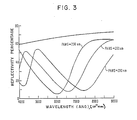
- Substrate 10 Composed of PMMA is 1.1 mm thick and transparent.
- First layer 11 Amorphous Si film is deposited by sputtering silicon 10 nm thick, in argon gas, at a pressure of 2.0 266,6 Pa (2.0 Torr) and at 25°C.
- Second layer 12 This layer is composed of Poly Alpha Methyl Styrene (PAMS) polymeric film with several different samples having thicknesses of 236 nm, 260 nm, and 290 nm respectively. This layer is formed by casting from a solvent, in which the polymer is dissolved.
- PAMS Poly Alpha Methyl Styrene
- Top layer 13 NiCrFe film 20 nm thick, deposited by sputtering in argon gas at 266.6 Pa (2.0 Torr) pressure, and 25°C. Layer 13 is continuous and mechanically strong, so that vesicles 15 can be formed in layer 13 by gas liberated from the dielectric layer 12 below layer 13.
- Fig. 3 is a plot of the percentage of reflectivity of the samples described in the above example as a function of the wavelength of the light in 10- 1 nm (Angstroms).
- the upper line is for reflectivity of NiCrFe layer 13 as measured for normal incidence of light upon surface 17 when light is shining down upon it from above.
- the lower three curves are measured for a beam 16 directed from below the substrate 10 onto surface 18 of the structure.
- a structure for an optimized 840 nm wavelength may be fabricated with layer 12 composed of a PAMS polymeric film having a thickness of 320 nm yielding a total reflectivity value of about 10%.
- an optical efficiency of greater than 70% is provided for absorption of light in the NiCrFe layer 13.
Landscapes
- Optical Record Carriers And Manufacture Thereof (AREA)
- Thermal Transfer Or Thermal Recording In General (AREA)
Claims (7)
Applications Claiming Priority (2)
| Application Number | Priority Date | Filing Date | Title |
|---|---|---|---|
| US06/500,513 US4578788A (en) | 1983-06-02 | 1983-06-02 | High performance optical storage medium with separate mechanical servo tracks embedded within the medium |
| US500513 | 1983-06-02 |
Publications (2)
| Publication Number | Publication Date |
|---|---|
| EP0130329A1 EP0130329A1 (de) | 1985-01-09 |
| EP0130329B1 true EP0130329B1 (de) | 1988-08-24 |
Family
ID=23989742
Family Applications (1)
| Application Number | Title | Priority Date | Filing Date |
|---|---|---|---|
| EP84105545A Expired EP0130329B1 (de) | 1983-06-02 | 1984-05-16 | Optisches Datenspeichermedium |
Country Status (4)
| Country | Link |
|---|---|
| US (1) | US4578788A (de) |
| EP (1) | EP0130329B1 (de) |
| JP (1) | JPS601634A (de) |
| DE (1) | DE3473669D1 (de) |
Families Citing this family (48)
| Publication number | Priority date | Publication date | Assignee | Title |
|---|---|---|---|---|
| US4719615A (en) * | 1983-08-22 | 1988-01-12 | Optical Data, Inc. | Erasable optical data storage medium |
| JPS60208289A (ja) * | 1984-03-31 | 1985-10-19 | Dainippon Printing Co Ltd | 光記録材料 |
| CA1241741A (en) * | 1984-05-24 | 1988-09-06 | Robert A. Scranton | Variable impedance contrast in data storage media |
| US4718053A (en) * | 1984-11-09 | 1988-01-05 | Hitachi, Ltd. | Optical information apparatus and method of recording and erasing information |
| US4782477A (en) * | 1985-09-30 | 1988-11-01 | Kabushiki Kaisha Toshiba | Optical recording medium with fluorine resin adhesive |
| US4731755A (en) * | 1986-04-10 | 1988-03-15 | International Business Machines Corporation | Thermal design for reversible phase change optical storage media |
| US4816841A (en) * | 1986-07-11 | 1989-03-28 | Kuraray Co., Ltd. | Optical recording medium |
| US4863819A (en) * | 1986-09-11 | 1989-09-05 | Drexler Technology Corporation | Read-only optical data card |
| IT1222105B (it) * | 1986-09-11 | 1990-08-31 | Drexler Tech | Scheda per dati ottici,a sola lettura |
| US4901304A (en) * | 1986-10-08 | 1990-02-13 | Optical Data, Inc. | Erasable optical data storage medium having a zoned integral recording layer |
| US4825430A (en) * | 1986-12-19 | 1989-04-25 | Optical Data, Inc. | Erasable optical data storage medium having an embedded servo track and a subsurface recording interface |
| EP0382713A1 (de) * | 1987-04-16 | 1990-08-22 | Drexler Technology Corporation | Optische speicherkarte mit vielfachspeichermitteln |
| US5036511A (en) * | 1988-02-05 | 1991-07-30 | Tandy Corporation | Recording method and apparatus |
| US5208801A (en) * | 1988-02-05 | 1993-05-04 | Tandy Corporation | Method and apparatus for correcting focus in an optical recording system |
| US5014259A (en) * | 1988-02-05 | 1991-05-07 | Tandy Corporation | Recording medium having an insulating layer |
| US4852077A (en) * | 1988-02-05 | 1989-07-25 | Tandy Corporation | Optical data storage media with spatially variable energy absorptivity |
| US5200948A (en) * | 1988-02-05 | 1993-04-06 | Tandy Corporation | Recording method and apparatus |
| US5016239A (en) * | 1988-02-05 | 1991-05-14 | Tandy Corporation | Recording method and apparatus |
| US5001699A (en) * | 1988-02-05 | 1991-03-19 | Tandy Corporation | Recording method and apparatus |
| AU622435B2 (en) * | 1988-02-05 | 1992-04-09 | Tandy Corporation | Optical data storage media with spatially variable energy absorptivity |
| US5018128A (en) * | 1988-02-05 | 1991-05-21 | Tandy Corporation | Apparatus and medium for recording erasable information |
| US5088088A (en) * | 1988-02-05 | 1992-02-11 | Tandy Corporation | Dye-polymer optical data storage media with improved recording sensitivity |
| US4896314A (en) * | 1988-04-19 | 1990-01-23 | Optical Data, Inc. | Bump-forming media including thin intermediate reflective layer and methods for writing, reading, and erasing same |
| JPH0378131A (ja) * | 1989-08-18 | 1991-04-03 | Brother Ind Ltd | 光記録媒体 |
| DE68921453T2 (de) * | 1988-12-28 | 1995-07-13 | Canon Kk | Informationsaufzeichnungsträger. |
| US5079758A (en) * | 1989-09-28 | 1992-01-07 | Tandy Corporation | Single polymer layer recordable/erasable optical media |
| US5175720A (en) * | 1989-05-25 | 1992-12-29 | Tandy Corporation | Interactive optical disk |
| WO1990014663A1 (en) * | 1989-05-25 | 1990-11-29 | Tandy Corporation | Interactive optical disk, method of fabrication and apparatus for recording thereon |
| US5134601A (en) * | 1989-08-08 | 1992-07-28 | International Business Machines Corporation | Optical disk sector servo patterns |
| US5099469A (en) * | 1990-02-20 | 1992-03-24 | Del Mar Avionics | Process for manufacturing an optical disc master |
| US5144613A (en) * | 1990-07-26 | 1992-09-01 | Tandy Corporation | Thermal bulk erasure method for dye polymer optical media |
| US5666344A (en) * | 1991-06-04 | 1997-09-09 | International Business Machines Corporation | Multiple data surface optical data storage system |
| US5406544A (en) * | 1991-07-25 | 1995-04-11 | Clark; Bryan K. | Low cost substrate for bump-forming recording media |
| JPH06511343A (ja) * | 1991-10-03 | 1994-12-15 | オーディーエムイー・インタナショナル・ビー・ヴィー | 光ディスク原盤 |
| US5455818A (en) * | 1992-01-22 | 1995-10-03 | Brother Kogyo Kabushiki Kaisha | Optical recording medium |
| TW273616B (de) * | 1993-12-15 | 1996-04-01 | Ibm | |
| US6539336B1 (en) * | 1996-12-12 | 2003-03-25 | Phatrat Technologies, Inc. | Sport monitoring system for determining airtime, speed, power absorbed and other factors such as drop distance |
| US5728441A (en) * | 1995-12-01 | 1998-03-17 | Samsung Electronics Co., Ltd. | Recordable/replayable optical recording medium and optical recording method therefor |
| US5925433A (en) * | 1995-12-01 | 1999-07-20 | Akzo Nobel N.V. | Optical recording medium based on Fabry-Perot principle |
| EP0777224B1 (de) * | 1995-12-01 | 2002-07-03 | Samsung Electronics Co., Ltd. | Optisches Aufzeichnungsmedium und optisches Aufzeichnungsverfahren |
| KR100230448B1 (ko) * | 1996-10-10 | 1999-11-15 | 윤종용 | 광기록매체 |
| KR100230449B1 (ko) * | 1996-10-10 | 1999-11-15 | 윤종용 | 광기록매체 |
| JPH11328724A (ja) * | 1998-05-18 | 1999-11-30 | Fuji Photo Film Co Ltd | 3次元光メモリ |
| US6540397B2 (en) * | 2000-04-07 | 2003-04-01 | Siro Technologies, Inc. | Optical information storage medium |
| US6731591B2 (en) * | 2000-08-01 | 2004-05-04 | Tdk Corporation | Optical information medium |
| US20020191501A1 (en) * | 2001-05-14 | 2002-12-19 | Matsushita Electric Industrial Co., Ltd. | Optical recording medium, optical pickup apparatus, and recording and reproducing apparatus |
| CN1591626A (zh) * | 2003-09-02 | 2005-03-09 | 皇家飞利浦电子股份有限公司 | 多层光盘及其制作方法 |
| FR2884032B1 (fr) * | 2005-03-29 | 2007-06-08 | Commissariat Energie Atomique | Support d'enregistrement optique irreversible par formation de bulles ayant une hauteur limitee par la source de gaz les generant |
Citations (1)
| Publication number | Priority date | Publication date | Assignee | Title |
|---|---|---|---|---|
| EP0124950A1 (de) * | 1983-05-09 | 1984-11-14 | Koninklijke Philips Electronics N.V. | Optisch schreibbarer und lesbarer Informationsträger |
Family Cites Families (15)
| Publication number | Priority date | Publication date | Assignee | Title |
|---|---|---|---|---|
| US4000492A (en) * | 1974-04-04 | 1976-12-28 | Bell Telephone Laboratories, Incorporated | Metal film recording media for laser writing |
| US4175145A (en) * | 1975-04-28 | 1979-11-20 | Teletype Corporation | Making memory structure for laser recording system |
| FR2365854A1 (fr) * | 1976-09-24 | 1978-04-21 | Thomson Brandt | Procede de fabrication d'un support d'information enregistrable et lisible optiquement et support obtenu par un tel procede |
| NL7802860A (nl) * | 1978-03-16 | 1979-09-18 | Philips Nv | Registratiedragerlichaam en registratiedrager voor optische informatie en inrichting voor het inschrijven en uitlezen. |
| NL7803069A (nl) * | 1978-03-22 | 1979-09-25 | Philips Nv | Meerlaags informatieschijf. |
| NL7906576A (nl) * | 1979-09-03 | 1981-03-05 | Philips Nv | Registratiedrager waarin informatie is aangebracht in een optisch uitleesbare informatiestruktuur, alsmede uitleesinrichting daarvoor. |
| NL7906728A (nl) * | 1979-09-10 | 1981-03-12 | Philips Nv | Optische registratieschijf. |
| US4285056A (en) * | 1979-10-17 | 1981-08-18 | Rca Corporation | Replicable optical recording medium |
| JPS5661048A (en) * | 1979-10-22 | 1981-05-26 | Nippon Telegr & Teleph Corp <Ntt> | Optical memory medium |
| FR2474222A1 (fr) * | 1980-01-23 | 1981-07-24 | Thomson Csf | Procede d'inscription thermo-optique d'information et support d'information destine a la mise en oeuvre de ce procede |
| NL8002039A (nl) * | 1980-04-08 | 1981-11-02 | Philips Nv | Optisch uitleesbare informatieschijf. |
| FR2490858B1 (fr) * | 1980-09-25 | 1986-04-04 | Rca Corp | Milieu d'enregistrement optique a sensibilite variable et disque contenant de l'information, realise a l'aide d'un tel milieu |
| JPS5760544A (en) * | 1980-09-30 | 1982-04-12 | Fujitsu Ltd | Optical information recording medium |
| JPS57158047A (en) * | 1981-03-24 | 1982-09-29 | Toshiba Corp | Optical information recording medium |
| US4451914A (en) * | 1982-04-15 | 1984-05-29 | Burroughs Corporation | Optical storage system employing a multi-layer optical medium |
-
1983
- 1983-06-02 US US06/500,513 patent/US4578788A/en not_active Expired - Lifetime
-
1984
- 1984-05-16 EP EP84105545A patent/EP0130329B1/de not_active Expired
- 1984-05-16 DE DE8484105545T patent/DE3473669D1/de not_active Expired
- 1984-05-29 JP JP59107673A patent/JPS601634A/ja active Granted
Patent Citations (1)
| Publication number | Priority date | Publication date | Assignee | Title |
|---|---|---|---|---|
| EP0124950A1 (de) * | 1983-05-09 | 1984-11-14 | Koninklijke Philips Electronics N.V. | Optisch schreibbarer und lesbarer Informationsträger |
Also Published As
| Publication number | Publication date |
|---|---|
| JPH0370862B2 (de) | 1991-11-11 |
| JPS601634A (ja) | 1985-01-07 |
| EP0130329A1 (de) | 1985-01-09 |
| US4578788A (en) | 1986-03-25 |
| DE3473669D1 (en) | 1988-09-29 |
Similar Documents
| Publication | Publication Date | Title |
|---|---|---|
| EP0130329B1 (de) | Optisches Datenspeichermedium | |
| US4998239A (en) | Optical information recording medium containing a metal alloy as a reflective material | |
| US6333914B1 (en) | Optical recording medium and method of manufacturing same | |
| US4852077A (en) | Optical data storage media with spatially variable energy absorptivity | |
| JPH0666093B2 (ja) | 記録媒体 | |
| US4918682A (en) | Ablative and bump-forming optical recording media including a metallic reflective layer | |
| GB2084786A (en) | Variable sensitivity optical recording medium and information record | |
| JPH09326136A (ja) | 光記録媒体及びその製造方法 | |
| EP0345273B1 (de) | Medium für optische aufzeichnung | |
| US4547876A (en) | Optical recording medium and information record and method of making same | |
| JPH0821178B2 (ja) | 光学記録媒体 | |
| WO2003075268A1 (en) | Optical information recording medium | |
| CA2239067A1 (en) | Optical recording medium based on fabry-perot principle | |
| JPH113543A (ja) | 情報記録媒体 | |
| JPH0850739A (ja) | 光学的情報記録媒体 | |
| JPH11345431A (ja) | 情報記録媒体 | |
| JP2002342980A (ja) | 光情報記録媒体 | |
| JP3139479B2 (ja) | 情報記録媒体、情報記録媒体の製造方法、情報の記録・再生方法、及び、情報の消去方法 | |
| JP2006085845A (ja) | 多層光情報記録媒体及び光情報記録再生装置 | |
| JP2001067727A (ja) | 光ディスク | |
| JP2005092927A (ja) | 多層光ディスク | |
| JP2940176B2 (ja) | 光学記録媒体およびその記録再生方法 | |
| US5966363A (en) | Optical and magneto-optic data storage systems utilizing transmissive media | |
| JPH09288846A (ja) | 情報記録媒体及びその再生方法 | |
| KR0159549B1 (ko) | 2층 기록구조를 갖는 광기록매체 및 그 제조방법 |
Legal Events
| Date | Code | Title | Description |
|---|---|---|---|
| PUAI | Public reference made under article 153(3) epc to a published international application that has entered the european phase |
Free format text: ORIGINAL CODE: 0009012 |
|
| AK | Designated contracting states |
Designated state(s): DE FR GB |
|
| 17P | Request for examination filed |
Effective date: 19841123 |
|
| 17Q | First examination report despatched |
Effective date: 19860421 |
|
| GRAA | (expected) grant |
Free format text: ORIGINAL CODE: 0009210 |
|
| AK | Designated contracting states |
Kind code of ref document: B1 Designated state(s): DE FR GB |
|
| REF | Corresponds to: |
Ref document number: 3473669 Country of ref document: DE Date of ref document: 19880929 |
|
| ET | Fr: translation filed | ||
| PLBE | No opposition filed within time limit |
Free format text: ORIGINAL CODE: 0009261 |
|
| STAA | Information on the status of an ep patent application or granted ep patent |
Free format text: STATUS: NO OPPOSITION FILED WITHIN TIME LIMIT |
|
| 26N | No opposition filed | ||
| PGFP | Annual fee paid to national office [announced via postgrant information from national office to epo] |
Ref country code: GB Payment date: 19920409 Year of fee payment: 9 |
|
| PGFP | Annual fee paid to national office [announced via postgrant information from national office to epo] |
Ref country code: FR Payment date: 19920427 Year of fee payment: 9 |
|
| PGFP | Annual fee paid to national office [announced via postgrant information from national office to epo] |
Ref country code: DE Payment date: 19920523 Year of fee payment: 9 |
|
| PG25 | Lapsed in a contracting state [announced via postgrant information from national office to epo] |
Ref country code: GB Effective date: 19930516 |
|
| GBPC | Gb: european patent ceased through non-payment of renewal fee |
Effective date: 19930516 |
|
| PG25 | Lapsed in a contracting state [announced via postgrant information from national office to epo] |
Ref country code: FR Effective date: 19940131 |
|
| PG25 | Lapsed in a contracting state [announced via postgrant information from national office to epo] |
Ref country code: DE Effective date: 19940201 |
|
| REG | Reference to a national code |
Ref country code: FR Ref legal event code: ST |