EP0130468A2 - Protective coatings for conductors to prevent mechanical and electronic failures particularly during heat-treatment of their supporting structures - Google Patents
Protective coatings for conductors to prevent mechanical and electronic failures particularly during heat-treatment of their supporting structures Download PDFInfo
- Publication number
- EP0130468A2 EP0130468A2 EP84107040A EP84107040A EP0130468A2 EP 0130468 A2 EP0130468 A2 EP 0130468A2 EP 84107040 A EP84107040 A EP 84107040A EP 84107040 A EP84107040 A EP 84107040A EP 0130468 A2 EP0130468 A2 EP 0130468A2
- Authority
- EP
- European Patent Office
- Prior art keywords
- layer
- copper
- cop
- conductors
- protective coating
- Prior art date
- Legal status (The legal status is an assumption and is not a legal conclusion. Google has not performed a legal analysis and makes no representation as to the accuracy of the status listed.)
- Granted
Links
Images

Classifications
-
- H—ELECTRICITY
- H05—ELECTRIC TECHNIQUES NOT OTHERWISE PROVIDED FOR
- H05K—PRINTED CIRCUITS; CASINGS OR CONSTRUCTIONAL DETAILS OF ELECTRIC APPARATUS; MANUFACTURE OF ASSEMBLAGES OF ELECTRICAL COMPONENTS
- H05K3/00—Apparatus or processes for manufacturing printed circuits
- H05K3/22—Secondary treatment of printed circuits
- H05K3/24—Reinforcing of the conductive pattern
- H05K3/244—Finish plating of conductors, especially of copper conductors, e.g. for pads or lands
-
- C—CHEMISTRY; METALLURGY
- C23—COATING METALLIC MATERIAL; COATING MATERIAL WITH METALLIC MATERIAL; CHEMICAL SURFACE TREATMENT; DIFFUSION TREATMENT OF METALLIC MATERIAL; COATING BY VACUUM EVAPORATION, BY SPUTTERING, BY ION IMPLANTATION OR BY CHEMICAL VAPOUR DEPOSITION, IN GENERAL; INHIBITING CORROSION OF METALLIC MATERIAL OR INCRUSTATION IN GENERAL
- C23C—COATING METALLIC MATERIAL; COATING MATERIAL WITH METALLIC MATERIAL; SURFACE TREATMENT OF METALLIC MATERIAL BY DIFFUSION INTO THE SURFACE, BY CHEMICAL CONVERSION OR SUBSTITUTION; COATING BY VACUUM EVAPORATION, BY SPUTTERING, BY ION IMPLANTATION OR BY CHEMICAL VAPOUR DEPOSITION, IN GENERAL
- C23C30/00—Coating with metallic material characterised only by the composition of the metallic material, i.e. not characterised by the coating process
-
- H—ELECTRICITY
- H05—ELECTRIC TECHNIQUES NOT OTHERWISE PROVIDED FOR
- H05K—PRINTED CIRCUITS; CASINGS OR CONSTRUCTIONAL DETAILS OF ELECTRIC APPARATUS; MANUFACTURE OF ASSEMBLAGES OF ELECTRICAL COMPONENTS
- H05K3/00—Apparatus or processes for manufacturing printed circuits
- H05K3/38—Improvement of the adhesion between the insulating substrate and the metal
- H05K3/382—Improvement of the adhesion between the insulating substrate and the metal by special treatment of the metal
- H05K3/384—Improvement of the adhesion between the insulating substrate and the metal by special treatment of the metal by plating
-
- H—ELECTRICITY
- H05—ELECTRIC TECHNIQUES NOT OTHERWISE PROVIDED FOR
- H05K—PRINTED CIRCUITS; CASINGS OR CONSTRUCTIONAL DETAILS OF ELECTRIC APPARATUS; MANUFACTURE OF ASSEMBLAGES OF ELECTRICAL COMPONENTS
- H05K2203/00—Indexing scheme relating to apparatus or processes for manufacturing printed circuits covered by H05K3/00
- H05K2203/07—Treatments involving liquids, e.g. plating, rinsing
- H05K2203/0703—Plating
- H05K2203/072—Electroless plating, e.g. finish plating or initial plating
-
- H—ELECTRICITY
- H05—ELECTRIC TECHNIQUES NOT OTHERWISE PROVIDED FOR
- H05K—PRINTED CIRCUITS; CASINGS OR CONSTRUCTIONAL DETAILS OF ELECTRIC APPARATUS; MANUFACTURE OF ASSEMBLAGES OF ELECTRICAL COMPONENTS
- H05K3/00—Apparatus or processes for manufacturing printed circuits
- H05K3/46—Manufacturing multilayer circuits
- H05K3/4644—Manufacturing multilayer circuits by building the multilayer layer by layer, i.e. build-up multilayer circuits
Definitions
- This invention relates to protective coatings for conductors to prevent mechanical and electronic failures particularly during heat-treatment of their supporting structures.
- the invention has significant utility in the protection of Cu current-carrying lines in electronic structures that comprise multi layers that are subjected to heat treatments that would normally adversely affect the Cu lines.
- packages of microelectronic circuitry commonly comprise a substrate, at least one layer of copper current-carrying lines, at least one layer of an organic dielectric material (such as polyimide) which serves as an insulator, and additional layers of current- carrying lines.
- organic dielectric material such as polyimide
- these structures have to be heat- treated in order to cure the organic dielectric. During the curing cycles these organic materials often release water as a by-product. Also, even after these organic dielectrics are cured, they remain permeable to water and to other atmospheric contaminants. If the package incorporates copper or some other oxidizable or corrosible metal or alloy, the vulnerable metal must be protected in order to prevent the degradation of the circuitry over time.
- the potential number of suitable materials is severely limited by another requirement of the electronic package. It is often the situation that there is physical contact established between one metal or alloy and another. During the package processing steps, such as curing, soldering, and brazing, the structure is often exposed to thermal cycling for prolonged periods of time. Unless the regions of metal-to-metal contact are prevented from interdiffusion during the periods of thermal cycling, the electronic properties of the package will be altered. In particular, interdiffusion between metals will adversely affect the conductivity of the metals. For current-carrying lines of small dimensions, this is a particularly severe problem.
- the current-carrying lines have to be protected against all sorts of chemical attack, including oxidation, and must be protected against interdiffusion with other metals which the current- carrying lines contact.
- Chemical attack and interdiffusion will not only impair the conductivity of the current-carrying lines, but may also adversely affect the adhesion of these lines to an organic dielectric.
- an adhesion layer such as Cr
- the poor adhesion of copper to polyimide may be due to the formation of a loosely adhering copper oxide on the surface of the copper.
- Flexibility of fabrication is achieved if the coating that provides protection against chemical attack, protection against interdiffusion, and adhesion of the line is capable of electroless deposition. If the required which would also require an additional masking step.
- a coating of CoP is provided on Cu lines or other lines composed of corrosible materials, in order to protect the lines.
- the CoP layer can be made very thin and will protect the underlying lines from chemical attack and also from interdiffusion with other materials to which physical contact is made.
- an electronic package having a substrate, at least one layer of current-carrying lines composed of copper or another corrosible material, at least one insulating layer generally an organic dielectric, and a layer of CoP deposited on and in contact with the current-carrying lines.
- This structure can be subjected to heat treatments such as those used for curing, soldering, brazing, etc., without chemical attack of the copper or other corrosible materials.
- the CoP acts as an interdiffusion barrier between the lines and any other materials which are in contact with the CoP-protected lines. In a particular example, the CoP acts as an interdiffusion barrier between Cu and Au.
- the CoP can be present in many forms, including as a compound or an amorphous mixture, or a mixture of Co and CoP compound.
- the protective coating includes Co and P, and the P is present in amount at least about 2%, by weight.
- 8%P provides a suitable coating in a thickness of approximately 1000A.
- CoP can be electroplated or electrolessly plated, although electroless plating is a particular advantage, as previously pointed out.
- the use of CoP as a protective coating has a very important utility in microelectronic structures where the current-carrying lines are very small.
- a structure of particularly critical importance is one in which a substrate providing mechanical support, such as Si, ceramic, or glass has thereover a layer of thin copper lines, typically having widths of 6-50 micrometers and thicknesses 6-50 micrometers.
- the copper lines are protected by a coating of CoP having a thickness of about 500A or more.
- the CoP coating has a minimum thickness which will provide a continuous thin film and a maximum thickness normally set by the dimensions required for the electronic package.
- the protective coating must be continuous and of a thickness to prevent corrosion and interdiffusion (if necessary), and must not be so thick as to substantially alter the sizes required for the current-carrying lines. It is this microelectronic structure which forms a significant part of this invention.
- the invention provides an electrical structure comprising copper or copper based electrical conductors, characterised in that the conductors having a passivating coating layer containing cobalt (Co) and phosporous (P) .
- the invention also provides a multi-level structure comprising a first layer of copper, a second layer overlying said copper layer and protecting it from the environment, said second layer being comprised of Co and P and being thinner than said copper layer, and a third layer being comprised of a metal in contact with said second layer, said second layer substantially preventing interdiffusion between said first and third layers.
- a protective coating including Co and P will provide very effective protection against chemical attack of an underlying corrosible conductor, such as copper, and will also provide an effective interdiffusion barrier between the corrosible conductor and other metal layers which contact the conductor.
- This protection leads to an improved thin film package in which very thin and narrow conductor lines can be effectively used in a package containing layers of organic dielectric which package has to be heat treated for process steps such as curing, soldering, brazing, etc.
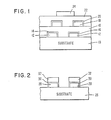
- FIGS. 1 and 2 represent typical structures in which protection against chemical attack and interdiffusion is required.
- a substrate 10 such as glass, ceramic, silicon, etc.
- a first conductive level comprising the conductors 12.
- These conductors are typically copper, an alloy of copper, or other materials which often contain copper.
- Conductors 12 are, therefore, composed of corrosible material.
- a thin protective coating layer 14, or cladding is deposited on the conductors 12.
- An insulating layer 16 typically an organic dielectric such as polyimide, is deposited over the protected conductors 12.
- another layer of corrosible conductors 18 would be provided which are also protected by a protective layer 20 of CoP.
- a second insulating layer 22 which also can be composed of an organic dielectric such as polyimide.
- a third conductive layer 24 is provided, which is used for other current-carrying or contact functions in the overall micro-electronic package represented by FIG. 1.
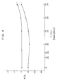
- FIG. 2 illustrates a structure in which the CoP protective layer is also used as an interdiffusion barrier.
- a substrate 26 similar to the substrate 10 of FIG. 1, has a layer of corrosible conductors 28 thereon. Again, these conductors are typically copper or an alloy of copper.
- a thin protective layer 30 of CoP is deposited on the conductors 28 and serves to protect them from chemical attack. Protective layer 30 also serves as an interdiffusion barrier between the conductors 28 and an overlying metal layer 32.
- conductors 28 can be comprised of copper or an alloy of copper, while metal layer 32 can be another conductor such as gold.
- the CoP protection layer prevents interdiffusion between conductor 28 and metal layer 32.
- CoP provides a very effective interdiffusion barrier between copper and gold.
- the types of conductors that are protected by the CoP protective layer include any type of conductor that is more corrosible than CoP, and is particularly exemplified by conductors comprising copper or alloys of copper.
- the invention has for a primary object the protection of conductors which contain copper, the protection being against any type of corrosive attack as well as against interdiffusion with other metals.
- the CoP protective material can take any structural form, including amorphous and crystalline structures.
- a compound of cobalt and phosphorous is suitable, as well as alloys, mixtures of Co and compounds of CoP, and mixtures including Co and P.
- the protective layer has to be pinhole free and continuous in order to provide the protective function, and its thickness is generally that which will provide protection against corrosion and protection against interdiffusion, if the conductor is to be contacted by another metal or any material with which it might interdiffuse.
- an alloy comprising 8% phosphorous with the remainder cobalt is particularly suitable at a thickness of about 1000 A.
- thicknesses down to about 500 A also appear to be suitable, and greater thicknesses than 1000 A can also be used.
- the upper limit on thickness is quite arbitrary.
- the percentage of phosphorous in the coating can be extended over a fairly wide range, and is generally about 2 to about 15%, by weight. These percentages have been found to be particularly useful when the copper is to be protected from corrosion and interdiffusion with other metals, such as gold. In particular, these percentages are particularly suitable for use in multi-layer structures comprising organic dielectrics and copper conductive lines of small dimensions.
- An advantage of the present invention is that the protective properties of layers containing Co and P are not very sensitive to the amount of P which is present. Generally, at temperatures less than about 400°C, interdiffusion between copper and a contacting metal proceeds by grain boundary diffusion. As the CoP-clad copper film is heated, Co 3 P precipitates in increasing amounts in the grain boundaries, thereby effectively blocking the grain boundary diffusion process.
- the CoP protective layer can be electrolessly deposited on the three exposed sides of the conductor lines.
- a Pd catalyst is first deposited.
- This treatment will give a Pd coverage on the copper of ⁇ 0.5ug/cm2.
- This procedure gives good coverage of the copper, but in the plating of patterned copper lines, metal deposition sometimes occurs on the organic dielectric between closely spaced lines (so-called extraneous deposition or bridging).
- a rinse is sometimes used between the Pd activation step and the electroless deposition of CoP.
- This rinse is either an aqueous NH 3 solution of pH 11.2 or a 0.2M EDTA solution of pH 7.0 (pH adjusted with NaOH).
- a representative solution for electroless deposition of CoP, 8%P has the following composition:
- Resistance measurements were also used to indicate loss of conducting copper metal by oxidation during curing of polyimide, which is a commonly used organic dielectric in electric and electronic packaging.
- Some sheet samples were measured with a standard 4-point probe by scraping away some of the polyimide at the center of the sample. Since this scraping procedure may damage copper in the vicinity of the probe and thus adversely affect the resistance measurement, the method of Van der Pauw was used (Phillips Res. Repts., 13, 1, 1958) to measure the resistance of the sheet samples. That method involves removal of polyimide to form four arbitrarily placed contacts on the circumference of the sample. Pattern samples were also prepared for 4-point probe measurement of the increase of resistance of a copper line upon polyimide cure.
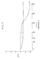
- FIG. 3 shows the dependence of the relative resistivity of an unprotected copper film upon annealing. The time the sample remains at each temperature is given in parentheses. The sample consisted of 2.2mm of electroplated copper on a substrate with an evaporated plating base consisting of 200A of Nb and 100A of copper. The observed behavior is that expected when the adhesion layer does not diffuse into the copper.
- Packaging structures commonly use Cr to give adhesion of copper lines to dielectrics and to protect copper against corrosion.
- FIGS. 4-7 should be compared to Cr, which is also illustrated in FIG. 3. Under the conditions of this annealing cycle, the resistivity of Cr-clad copper is always somewhat higher than that of pure copper.
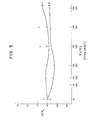
- FIG. 3 shows the relative resistivity behavior when a layer of Ni of thickness 1000A is deposited on copper.
- the curves are indistinguishable for evaporated and electroplated Ni.
- the annealing cycle was begun again at room temperature to yield curve 2. Further annealing for five hours at 400°C gave point 3.
- the increase in resistivity of this sample indicates extensive interdiffusion of the copper and nickel, and therefore indicates that nickel is a poor protective coating.
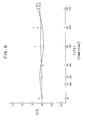
- FIGS. 5 and 6 illustrate the situation for protective coatings of NiP and NiB which were electrolessly plated.
- FIG. 6 shows films with higher B and P content than those in FIG. 5. These electroless Ni alloys interdiffuse less extensively with copper than does pure Ni. A clear-cut dependence on P or B concentration was not observed.
- FIG. 7 illustrates the use of a protective layer of Co and a protective layer of CoP containing 8% P, by weight. Pure Co interdiffuses with copper to a lesser extent than does pure Ni.
- FIG. 7 shows the best result obtained upon annealing of Co-coated Cu. Cobalt gives less resistivity rise than Cr (FIG. 3). However, alloying of Co with P through electroless deposition leads to even more favorable behavior.
- the curve for CoP with 8% by weight P in FIG. 7 is nearly identical to the curve for unprotected Cu in FIG. 3. Since annealing, by itself, will cause a decrease in resistivity of copper (due to effects of crystallinity, etc.), the reference base for the value of the coating is the lower curve in FIG. 3, indicating the behavior of copper in this annealing cycle. As is apparent from a comparison of FIGS. 3 and 7, only CoP provides a protection indicative of substantially no interdiffusion.
- films containing Co and P were found to provide vastly superior protection of corrosible conductors, especially those having copper therein. This protection was observed even during harsh annealing cycles, such as those used to provide electronic packages.
Landscapes
- Engineering & Computer Science (AREA)
- Chemical & Material Sciences (AREA)
- Microelectronics & Electronic Packaging (AREA)
- Manufacturing & Machinery (AREA)
- Organic Chemistry (AREA)
- Metallurgy (AREA)
- Mechanical Engineering (AREA)
- Materials Engineering (AREA)
- Chemical Kinetics & Catalysis (AREA)
- Parts Printed On Printed Circuit Boards (AREA)
- Electrodes Of Semiconductors (AREA)
- Non-Metallic Protective Coatings For Printed Circuits (AREA)
- Manufacturing Of Printed Wiring (AREA)
- Chemically Coating (AREA)
Abstract
Description
- This invention relates to protective coatings for conductors to prevent mechanical and electronic failures particularly during heat-treatment of their supporting structures. The invention has significant utility in the protection of Cu current-carrying lines in electronic structures that comprise multi layers that are subjected to heat treatments that would normally adversely affect the Cu lines.
- Current-carrying lines are often fabricated from materials such as copper and its alloys, which are readily corrosible in different atmospheres. In particular, packages of microelectronic circuitry commonly comprise a substrate, at least one layer of copper current-carrying lines, at least one layer of an organic dielectric material (such as polyimide) which serves as an insulator, and additional layers of current- carrying lines. These structures have to be heat- treated in order to cure the organic dielectric. During the curing cycles these organic materials often release water as a by-product. Also, even after these organic dielectrics are cured, they remain permeable to water and to other atmospheric contaminants. If the package incorporates copper or some other oxidizable or corrosible metal or alloy, the vulnerable metal must be protected in order to prevent the degradation of the circuitry over time.
- Although many possible protective coating materials can be envisioned, the potential number of suitable materials is severely limited by another requirement of the electronic package. It is often the situation that there is physical contact established between one metal or alloy and another. During the package processing steps, such as curing, soldering, and brazing, the structure is often exposed to thermal cycling for prolonged periods of time. Unless the regions of metal-to-metal contact are prevented from interdiffusion during the periods of thermal cycling, the electronic properties of the package will be altered. In particular, interdiffusion between metals will adversely affect the conductivity of the metals. For current-carrying lines of small dimensions, this is a particularly severe problem.
- Thus, the current-carrying lines have to be protected against all sorts of chemical attack, including oxidation, and must be protected against interdiffusion with other metals which the current- carrying lines contact. Chemical attack and interdiffusion will not only impair the conductivity of the current-carrying lines, but may also adversely affect the adhesion of these lines to an organic dielectric. For example, it is known in the art that polyimides do not adhere well to copper, and consequently an adhesion layer (such as Cr) is used between the copper and the polyimide. The poor adhesion of copper to polyimide may be due to the formation of a loosely adhering copper oxide on the surface of the copper.
- These problems are generally known in the art, and reference is made to the following examples of background art:
- J. E. Turn and E. L. Owen, "Metallic Diffusion Barriers for the Copper-Electrodeposited Gold System", AES Research Project, Plating, November 1974, at page 1915.
- M. R. Pinnel et al, "Mass Diffusion in Polycrystalline Copper/Electroplated Gold Planar Couples", Metallurgical Transactions, Vol. 3, July 1972, p. 1989.
- R. W. Lindsay et al, "The Structure and Mechanical Properties of Electroless Nickel", J. Electrochemical Soc., Vol. 112, No. 4, p. 401, April, 1965. U. S. Patents 4,065,588 and 4,188,438
- Flexibility of fabrication is achieved if the coating that provides protection against chemical attack, protection against interdiffusion, and adhesion of the line is capable of electroless deposition. If the required which would also require an additional masking step.
- In addition, protecting a line by plating through a mask would only cover the top of the line; electroless deposition protects all sides. After electroplating, a step to remove the contact layer would be required. Since the current-carrying lines are often extremely small, it is difficult to provide electrical contact to them for electroplating. Even if electrical lands are provided, the IR drop is great with extremely long and small lines, so the amount of current available for plating would be restricted and poor plating would often result. Thus, use of a material capable of electroless plating deposition provides a simpler method of protecting all of the exposed sides of the corrosible line. The use of techniques such as evaporation and sputtering for the deposition of the coating layer is not sufficient, since all three exposed sides of the corrosible material will not be protected.
- Accordingly, it is an object of this invention to provide a material that offers good protection against chemical attack of underlying copper or other corrosible lines and that prevents interdiffusion between the copper or other corrosible material and any metal or alloy with which it may be in contact.
- It is another object of this invention to provide an improved coating material that can be used to prevent chemical attack of corrosible lines and interdiffusion between these lines and other contacting metals.
- It is another object of this invention to provide an improved protective coating material for use with copper lines, which will protect the copper lines from all types of chemical attack.
- It is another object of this invention to provide a material that will protect copper lines from corrosive chemical attack, and that can be used as an interdiffusion barrier between the copper lines and other metals.
- It is a further object of the present invention to protect copper lines using a coating layer that can be electrolessly deposited.
- It is another object of this invention to provide an improved coating material for copper lines, which is effective when electrolessly deposited in thin layers.
- It is another object of this invention to provide an improved electronic package that contains organic dielectric material and current carrying metallic lines, where the metallic lines are protected against corrosion and interdiffusion by an improved layer of protective material. It is a further object of this invention to provide an improved protective coating for copper and other corrosible materials, which coating can be deposited as a thin film and which will prevent chemical attack of the copper or corrosible material and also interdiffusion between the copper or other corrosible material and other metals.
- It is a further object of this invention to provide a protective coating layer of CoP on Cu lines.
- It is another object of the present invention to provide an improved interdiffusion barrier that can be used between copper and other metals, such as gold, and that will prevent interdiffusion betweeen the copper and these other metals.
- In the broadest aspect of this invention, a coating of CoP is provided on Cu lines or other lines composed of corrosible materials, in order to protect the lines. The CoP layer can be made very thin and will protect the underlying lines from chemical attack and also from interdiffusion with other materials to which physical contact is made.
- In another aspect of this invention, an electronic package is provided having a substrate, at least one layer of current-carrying lines composed of copper or another corrosible material, at least one insulating layer generally an organic dielectric, and a layer of CoP deposited on and in contact with the current-carrying lines. This structure can be subjected to heat treatments such as those used for curing, soldering, brazing, etc., without chemical attack of the copper or other corrosible materials. Further, the CoP acts as an interdiffusion barrier between the lines and any other materials which are in contact with the CoP-protected lines. In a particular example, the CoP acts as an interdiffusion barrier between Cu and Au.
- The CoP can be present in many forms, including as a compound or an amorphous mixture, or a mixture of Co and CoP compound. In general, the protective coating includes Co and P, and the P is present in amount at least about 2%, by weight. As an example, 8%P provides a suitable coating in a thickness of approximately 1000A.
- CoP can be electroplated or electrolessly plated, although electroless plating is a particular advantage, as previously pointed out. The use of CoP as a protective coating has a very important utility in microelectronic structures where the current-carrying lines are very small. For example, a structure of particularly critical importance is one in which a substrate providing mechanical support, such as Si, ceramic, or glass has thereover a layer of thin copper lines, typically having widths of 6-50 micrometers and thicknesses 6-50 micrometers. The copper lines are protected by a coating of CoP having a thickness of about 500A or more. The CoP coating has a minimum thickness which will provide a continuous thin film and a maximum thickness normally set by the dimensions required for the electronic package. That is, the protective coating must be continuous and of a thickness to prevent corrosion and interdiffusion (if necessary), and must not be so thick as to substantially alter the sizes required for the current-carrying lines. It is this microelectronic structure which forms a significant part of this invention.
- The invention provides an electrical structure comprising copper or copper based electrical conductors, characterised in that the conductors having a passivating coating layer containing cobalt (Co) and phosporous (P) .
- The invention also provides a multi-level structure comprising a first layer of copper, a second layer overlying said copper layer and protecting it from the environment, said second layer being comprised of Co and P and being thinner than said copper layer, and a third layer being comprised of a metal in contact with said second layer, said second layer substantially preventing interdiffusion between said first and third layers.
- The invention will now be further described with reference to the accompanying drawings, in which:-
- FIG. 1 is an end view of a structure representative of the type in which the invention has particular utility, the structure being composed of a microelectronic package including at least one layer of a corrosible conductor which is protected by a layer including Co and P.
- FIG. 2 is an end view of a representative structure in which a coating including Co and P is used to protect a corrosible conductor and also to prevent interdiffusion between the conductor and another metal.
- FIG. 3 is a plot showing the dependence of the relative resistivity ρ/ρo on an annealing cycle, various times and temperatures being shown for an annealed copper line which is uncoated, and an annealed copper line which has a coating of Cr.
- FIG. 4 is a plot showing the dependence of the relative resistivity p/p on an annealing cycle of a copper conductor which is protected by a Ni coating. The sample was subjected to the annealing cycle two times.
- FIG. 5 is a plot of the dependence of the relative resistivity p/p for two copper conductors, one of which is covered with NiP and the other of which is covered with NiB, during an annealing cycle.
- FIG. 6 is a plot showing the dependence of relative resistivity p /p on an annealing cycle for two copper conductors, one of which is protected with a layer of NiP while the other is protected with a layer of NiB, where the compositions of NiP and NiB are different than the compositions of the corresponding protective coatings of FIG. 5.
- FIG. 7 is a plot of the dependence of relative resistivity P /P o of two copper conductors, one of which is protected by a coating of Co, while the other is protected by a coating of CoP in accordance with the present invention, during an annealing cycle. As is apparent from a comparison of FIGS. 3 and 7, the line protected by CoP has the lowest resistivity at the end of the annealing cycle.
- In the practice of this invention it has been discovered that a protective coating including Co and P will provide very effective protection against chemical attack of an underlying corrosible conductor, such as copper, and will also provide an effective interdiffusion barrier between the corrosible conductor and other metal layers which contact the conductor. This protection leads to an improved thin film package in which very thin and narrow conductor lines can be effectively used in a package containing layers of organic dielectric which package has to be heat treated for process steps such as curing, soldering, brazing, etc.
- FIGS. 1 and 2 represent typical structures in which protection against chemical attack and interdiffusion is required. In FIG. 1, a
substrate 10, such as glass, ceramic, silicon, etc., has thereon a first conductive level comprising theconductors 12. These conductors are typically copper, an alloy of copper, or other materials which often contain copper.Conductors 12 are, therefore, composed of corrosible material. For this reason, a thinprotective coating layer 14, or cladding, is deposited on theconductors 12. An insulatinglayer 16, typically an organic dielectric such as polyimide, is deposited over the protectedconductors 12. In many multi-layer packages, another layer ofcorrosible conductors 18 would be provided which are also protected by aprotective layer 20 of CoP. This is followed by the deposition of a second insulatinglayer 22 which also can be composed of an organic dielectric such as polyimide. Finally, a thirdconductive layer 24 is provided, which is used for other current-carrying or contact functions in the overall micro-electronic package represented by FIG. 1. - FIG. 2 illustrates a structure in which the CoP protective layer is also used as an interdiffusion barrier. In FIG. 2, a
substrate 26, similar to thesubstrate 10 of FIG. 1, has a layer ofcorrosible conductors 28 thereon. Again, these conductors are typically copper or an alloy of copper. A thinprotective layer 30 of CoP is deposited on theconductors 28 and serves to protect them from chemical attack.Protective layer 30 also serves as an interdiffusion barrier between theconductors 28 and anoverlying metal layer 32. For example,conductors 28 can be comprised of copper or an alloy of copper, whilemetal layer 32 can be another conductor such as gold. The CoP protection layer prevents interdiffusion betweenconductor 28 andmetal layer 32. In contrast with other protective layer compositions, such as those to be described with respect to FIGS. 3-7, CoP provides a very effective interdiffusion barrier between copper and gold. The types of conductors that are protected by the CoP protective layer include any type of conductor that is more corrosible than CoP, and is particularly exemplified by conductors comprising copper or alloys of copper. In particular, the invention has for a primary object the protection of conductors which contain copper, the protection being against any type of corrosive attack as well as against interdiffusion with other metals. - The CoP protective material can take any structural form, including amorphous and crystalline structures. A compound of cobalt and phosphorous is suitable, as well as alloys, mixtures of Co and compounds of CoP, and mixtures including Co and P. The protective layer has to be pinhole free and continuous in order to provide the protective function, and its thickness is generally that which will provide protection against corrosion and protection against interdiffusion, if the conductor is to be contacted by another metal or any material with which it might interdiffuse. As an example, an alloy comprising 8% phosphorous with the remainder cobalt is particularly suitable at a thickness of about 1000 A. However, thicknesses down to about 500 A also appear to be suitable, and greater thicknesses than 1000 A can also be used. Depending upon the structure in which the protective CoP coating is to be used, the upper limit on thickness is quite arbitrary.
- The percentage of phosphorous in the coating can be extended over a fairly wide range, and is generally about 2 to about 15%, by weight. These percentages have been found to be particularly useful when the copper is to be protected from corrosion and interdiffusion with other metals, such as gold. In particular, these percentages are particularly suitable for use in multi-layer structures comprising organic dielectrics and copper conductive lines of small dimensions. An advantage of the present invention is that the protective properties of layers containing Co and P are not very sensitive to the amount of P which is present. Generally, at temperatures less than about 400°C, interdiffusion between copper and a contacting metal proceeds by grain boundary diffusion. As the CoP-clad copper film is heated, Co3P precipitates in increasing amounts in the grain boundaries, thereby effectively blocking the grain boundary diffusion process. The CoP protective layer can be electrolessly deposited on the three exposed sides of the conductor lines. In order to initiate electroless deposition on copper, a Pd catalyst is first deposited. A ten second immersion in a room temperature solution of O.lg/l Pd C12,
pH 2 with HC1, followed by a thorough rinse, gives reliable initiation of the electroless process. This treatment will give a Pd coverage on the copper of < 0.5ug/cm2. This procedure gives good coverage of the copper, but in the plating of patterned copper lines, metal deposition sometimes occurs on the organic dielectric between closely spaced lines (so-called extraneous deposition or bridging). In an effort to reduce this extraneous deposition, a rinse is sometimes used between the Pd activation step and the electroless deposition of CoP. This rinse is either an aqueous NH3 solution of pH 11.2 or a 0.2M EDTA solution of pH 7.0 (pH adjusted with NaOH). A representative solution for electroless deposition of CoP, 8%P, has the following composition:
- References describing the electrodeposition of CoP alloys are U. S. Patents 3,073,762 and 3,202,590.
FIGS. 3-7 - These figures are various plots of the resistivity of copper lines, both protected and unprotected, measured as a function of annealing temperature, for different temperature-time intervals of the annealing cycle. In the evaluation of different cladding metals, an increase in resistivity relative to that of the unclad line is an indication of interdiffusion between the two metals. After each temperature-time interval of the anneal, the sample was cooled in vacuum to room temperature, and its sheet restivity p was measured using a 4-point probe. The resistivity varied from sample to sample because of variations of grain size, density, impurities, etc. For this reason, all results were normalized to the resistivity ρo the relative resistivity of the copper line is given by p/p , and the horizontal axes of the plots indicates the temperature (°C), while the numbers in parentheses below the temperatures indicate the times in minutes, at that temperature.
- Resistance measurements were also used to indicate loss of conducting copper metal by oxidation during curing of polyimide, which is a commonly used organic dielectric in electric and electronic packaging. Some sheet samples were measured with a standard 4-point probe by scraping away some of the polyimide at the center of the sample. Since this scraping procedure may damage copper in the vicinity of the probe and thus adversely affect the resistance measurement, the method of Van der Pauw was used (Phillips Res. Repts., 13, 1, 1958) to measure the resistance of the sheet samples. That method involves removal of polyimide to form four arbitrarily placed contacts on the circumference of the sample. Pattern samples were also prepared for 4-point probe measurement of the increase of resistance of a copper line upon polyimide cure.
- The interdiffusion between the various protective materials illustrated in FIGS. 3-7 and the copper line was studied by submitting examples to a vacuum anneal simulating the temperature excursions encountered in curing polyimide. The samples were annealed in a vacuum of 10-7 torr, in order to prevent the effects of interdiffusion of the metals from being confused by the effects due to oxidation.
- In order to determine the extent of interdiffusion between copper and the various cladding materials being evaluated, the annealing behavior of copper must first be known. FIG. 3 shows the dependence of the relative resistivity of an unprotected copper film upon annealing. The time the sample remains at each temperature is given in parentheses. The sample consisted of 2.2mm of electroplated copper on a substrate with an evaporated plating base consisting of 200A of Nb and 100A of copper. The observed behavior is that expected when the adhesion layer does not diffuse into the copper.
- Packaging structures commonly use Cr to give adhesion of copper lines to dielectrics and to protect copper against corrosion. Thus, the materials to be described with respects to FIGS. 4-7 should be compared to Cr, which is also illustrated in FIG. 3. Under the conditions of this annealing cycle, the resistivity of Cr-clad copper is always somewhat higher than that of pure copper.
- The use of Cr as protection on all exposed sides of a Cu line would entail the use of a complicated process, as has been mentioned earlier. Electrochemical studies of this system indicate that electroless deposition of Cr cannot be achieved without great difficulty, if at all.
- FIG. 3 shows the relative resistivity behavior when a layer of Ni of thickness 1000A is deposited on copper. The curves are indistinguishable for evaporated and electroplated Ni. After
curve 1 was obtained, the annealing cycle was begun again at room temperature to yieldcurve 2. Further annealing for five hours at 400°C gave point 3. The increase in resistivity of this sample indicates extensive interdiffusion of the copper and nickel, and therefore indicates that nickel is a poor protective coating. - FIGS. 5 and 6 illustrate the situation for protective coatings of NiP and NiB which were electrolessly plated. FIG. 6 shows films with higher B and P content than those in FIG. 5. These electroless Ni alloys interdiffuse less extensively with copper than does pure Ni. A clear-cut dependence on P or B concentration was not observed.
- FIG. 7 illustrates the use of a protective layer of Co and a protective layer of CoP containing 8% P, by weight. Pure Co interdiffuses with copper to a lesser extent than does pure Ni. FIG. 7 shows the best result obtained upon annealing of Co-coated Cu. Cobalt gives less resistivity rise than Cr (FIG. 3). However, alloying of Co with P through electroless deposition leads to even more favorable behavior. As is apparent, the curve for CoP with 8% by weight P in FIG. 7 is nearly identical to the curve for unprotected Cu in FIG. 3. Since annealing, by itself, will cause a decrease in resistivity of copper (due to effects of crystallinity, etc.), the reference base for the value of the coating is the lower curve in FIG. 3, indicating the behavior of copper in this annealing cycle. As is apparent from a comparison of FIGS. 3 and 7, only CoP provides a protection indicative of substantially no interdiffusion.
- In FIG. 7, a second annealing cycle does not result in a rise in resistivity. After an additional four and one half hours at 400°C, the P /P was 0.81. Thus, these annealing studies indicate that CoP is vastly superior to other protective cladding materials. CoP was also found to give good bond strength in ultrasonic bonding of Au-coated CdCu wires.
- In the practice of this invention films containing Co and P were found to provide vastly superior protection of corrosible conductors, especially those having copper therein. This protection was observed even during harsh annealing cycles, such as those used to provide electronic packages.
Claims (18)
Applications Claiming Priority (2)
| Application Number | Priority Date | Filing Date | Title |
|---|---|---|---|
| US50974283A | 1983-06-30 | 1983-06-30 | |
| US509742 | 1995-08-01 |
Publications (3)
| Publication Number | Publication Date |
|---|---|
| EP0130468A2 true EP0130468A2 (en) | 1985-01-09 |
| EP0130468A3 EP0130468A3 (en) | 1987-06-16 |
| EP0130468B1 EP0130468B1 (en) | 1989-04-19 |
Family
ID=24027910
Family Applications (1)
| Application Number | Title | Priority Date | Filing Date |
|---|---|---|---|
| EP19840107040 Expired EP0130468B1 (en) | 1983-06-30 | 1984-06-20 | Protective coatings for conductors to prevent mechanical and electronic failures particularly during heat-treatment of their supporting structures |
Country Status (3)
| Country | Link |
|---|---|
| EP (1) | EP0130468B1 (en) |
| JP (1) | JPS6010796A (en) |
| DE (1) | DE3477868D1 (en) |
Cited By (1)
| Publication number | Priority date | Publication date | Assignee | Title |
|---|---|---|---|---|
| WO2003085735A1 (en) * | 2002-04-02 | 2003-10-16 | Infineon Technologies Ag | Beol process for cu metallizations free from al-wirebond pads |
Families Citing this family (2)
| Publication number | Priority date | Publication date | Assignee | Title |
|---|---|---|---|---|
| JPS6211000A (en) * | 1985-07-08 | 1987-01-19 | Sonotetsuku:Kk | Ultrasonic oscillating electrode meson with flexible terminal |
| EP3607108A4 (en) * | 2017-04-04 | 2021-03-24 | Nanyang Technological University | CLADDED OBJECT AND METHOD FOR MOLDING IT |
Family Cites Families (4)
| Publication number | Priority date | Publication date | Assignee | Title |
|---|---|---|---|---|
| US3202590A (en) * | 1960-08-19 | 1965-08-24 | Ibm | Electrodeposition of cobalt-phosphorus alloys |
| US3073762A (en) * | 1960-08-22 | 1963-01-15 | Ibm | Electrodeposition of cobalt phosphorus alloys |
| JPS56155592A (en) * | 1980-04-03 | 1981-12-01 | Furukawa Circuit Foil | Copper foil for printed circuit and method of manufacturing same |
| JPS57145351A (en) * | 1981-03-04 | 1982-09-08 | Hitachi Cable Ltd | Lead frame for semiconductor |
-
1984
- 1984-04-19 JP JP7767284A patent/JPS6010796A/en active Granted
- 1984-06-20 DE DE8484107040T patent/DE3477868D1/en not_active Expired
- 1984-06-20 EP EP19840107040 patent/EP0130468B1/en not_active Expired
Cited By (1)
| Publication number | Priority date | Publication date | Assignee | Title |
|---|---|---|---|---|
| WO2003085735A1 (en) * | 2002-04-02 | 2003-10-16 | Infineon Technologies Ag | Beol process for cu metallizations free from al-wirebond pads |
Also Published As
| Publication number | Publication date |
|---|---|
| DE3477868D1 (en) | 1989-05-24 |
| EP0130468B1 (en) | 1989-04-19 |
| JPS6412116B2 (en) | 1989-02-28 |
| JPS6010796A (en) | 1985-01-19 |
| EP0130468A3 (en) | 1987-06-16 |
Similar Documents
| Publication | Publication Date | Title |
|---|---|---|
| US4717591A (en) | Prevention of mechanical and electronic failures in heat-treated structures | |
| US5164332A (en) | Diffusion barrier for copper features | |
| US3881884A (en) | Method for the formation of corrosion resistant electronic interconnections | |
| US7081680B2 (en) | Self-aligned corrosion stop for copper C4 and wirebond | |
| KR100228414B1 (en) | Aluminum alloy wiring layer manufacturing thereof,and aluminum alloy sputtering target | |
| US4319264A (en) | Nickel-gold-nickel conductors for solid state devices | |
| JPWO1992013360A1 (en) | Aluminum alloy wiring layer, manufacturing method thereof, and aluminum alloy sputtering target | |
| EP0030634B1 (en) | Nickel-x/gold/nickel-x conductors for solid state devices | |
| US4235648A (en) | Method for immersion plating very thin films of aluminum | |
| EP0130468B1 (en) | Protective coatings for conductors to prevent mechanical and electronic failures particularly during heat-treatment of their supporting structures | |
| Morabito et al. | Material characterization of Ti-Cu-Ni-Au (TCNA)-a new low cost thin film conductor system | |
| JP2505480B2 (en) | Copper alloy foil for flexible circuit boards | |
| KR900003849B1 (en) | Circuit substrate and thermal printing head using the same caller identifying method | |
| US5928568A (en) | Thick film circuit having conductor composition with coated metallic particles | |
| JP2534434B2 (en) | Oxidation resistant compound and method for producing the same | |
| US20010013651A1 (en) | Semiconductor device and manufacturing method therefor | |
| EP0344504B1 (en) | Article comprising a polyimide and a metal layer and methods of making such articles | |
| Young et al. | Improved characteristics of electroless Cu deposition on Pt–Ag metallized Al2O3 substrates in microelectronics packaging | |
| JP2000178793A (en) | Manufacturing method of metal polyimide substrate | |
| US5475265A (en) | Semiconductor device including gold interconnections where the gold grain size is a function of the width of the interconnections | |
| JPS625358B2 (en) | ||
| TW202545256A (en) | Wiring circuit board and manufacturing method of wiring circuit board | |
| JPH1032378A (en) | Printed wiring board for bonding | |
| Loos et al. | Influence of heat treatments on the electrical resistance of thin film copper/electroless nickel microcircuit interconnections | |
| JPS63254685A (en) | Electric contact device with nickel base |
Legal Events
| Date | Code | Title | Description |
|---|---|---|---|
| PUAI | Public reference made under article 153(3) epc to a published international application that has entered the european phase |
Free format text: ORIGINAL CODE: 0009012 |
|
| AK | Designated contracting states |
Designated state(s): DE FR GB |
|
| 17P | Request for examination filed |
Effective date: 19841123 |
|
| PUAL | Search report despatched |
Free format text: ORIGINAL CODE: 0009013 |
|
| AK | Designated contracting states |
Kind code of ref document: A3 Designated state(s): DE FR GB |
|
| 17Q | First examination report despatched |
Effective date: 19871023 |
|
| GRAA | (expected) grant |
Free format text: ORIGINAL CODE: 0009210 |
|
| AK | Designated contracting states |
Kind code of ref document: B1 Designated state(s): DE FR GB |
|
| REF | Corresponds to: |
Ref document number: 3477868 Country of ref document: DE Date of ref document: 19890524 |
|
| ET | Fr: translation filed | ||
| PLBE | No opposition filed within time limit |
Free format text: ORIGINAL CODE: 0009261 |
|
| STAA | Information on the status of an ep patent application or granted ep patent |
Free format text: STATUS: NO OPPOSITION FILED WITHIN TIME LIMIT |
|
| 26N | No opposition filed | ||
| PGFP | Annual fee paid to national office [announced via postgrant information from national office to epo] |
Ref country code: GB Payment date: 19920506 Year of fee payment: 9 |
|
| PGFP | Annual fee paid to national office [announced via postgrant information from national office to epo] |
Ref country code: FR Payment date: 19920601 Year of fee payment: 9 |
|
| PGFP | Annual fee paid to national office [announced via postgrant information from national office to epo] |
Ref country code: DE Payment date: 19920619 Year of fee payment: 9 |
|
| PG25 | Lapsed in a contracting state [announced via postgrant information from national office to epo] |
Ref country code: GB Effective date: 19930620 |
|
| GBPC | Gb: european patent ceased through non-payment of renewal fee |
Effective date: 19930620 |
|
| PG25 | Lapsed in a contracting state [announced via postgrant information from national office to epo] |
Ref country code: FR Effective date: 19940228 |
|
| PG25 | Lapsed in a contracting state [announced via postgrant information from national office to epo] |
Ref country code: DE Effective date: 19940301 |
|
| REG | Reference to a national code |
Ref country code: FR Ref legal event code: ST |