EP0130859B1 - Dispositif de déflexion d'un faisceau infra-rouge à commande électronique - Google Patents
Dispositif de déflexion d'un faisceau infra-rouge à commande électronique Download PDFInfo
- Publication number
- EP0130859B1 EP0130859B1 EP19840401027 EP84401027A EP0130859B1 EP 0130859 B1 EP0130859 B1 EP 0130859B1 EP 19840401027 EP19840401027 EP 19840401027 EP 84401027 A EP84401027 A EP 84401027A EP 0130859 B1 EP0130859 B1 EP 0130859B1
- Authority
- EP
- European Patent Office
- Prior art keywords
- waveguides
- waveguide
- electrodes
- electrode
- electro
- Prior art date
- Legal status (The legal status is an assumption and is not a legal conclusion. Google has not performed a legal analysis and makes no representation as to the accuracy of the status listed.)
- Expired
Links
- 239000000463 material Substances 0.000 description 6
- 230000003287 optical effect Effects 0.000 description 6
- 230000005855 radiation Effects 0.000 description 5
- 239000000758 substrate Substances 0.000 description 5
- JBRZTFJDHDCESZ-UHFFFAOYSA-N AsGa Chemical compound [As]#[Ga] JBRZTFJDHDCESZ-UHFFFAOYSA-N 0.000 description 3
- 230000008878 coupling Effects 0.000 description 3
- 238000010168 coupling process Methods 0.000 description 3
- 238000005859 coupling reaction Methods 0.000 description 3
- 238000009792 diffusion process Methods 0.000 description 3
- 238000000034 method Methods 0.000 description 3
- 230000003071 parasitic effect Effects 0.000 description 3
- CURLTUGMZLYLDI-UHFFFAOYSA-N Carbon dioxide Chemical compound O=C=O CURLTUGMZLYLDI-UHFFFAOYSA-N 0.000 description 2
- 229910001218 Gallium arsenide Inorganic materials 0.000 description 2
- 238000010521 absorption reaction Methods 0.000 description 2
- 229910052782 aluminium Inorganic materials 0.000 description 2
- XAGFODPZIPBFFR-UHFFFAOYSA-N aluminium Chemical compound [Al] XAGFODPZIPBFFR-UHFFFAOYSA-N 0.000 description 2
- 230000001427 coherent effect Effects 0.000 description 2
- 238000000407 epitaxy Methods 0.000 description 2
- GQYHUHYESMUTHG-UHFFFAOYSA-N lithium niobate Chemical compound [Li+].[O-][Nb](=O)=O GQYHUHYESMUTHG-UHFFFAOYSA-N 0.000 description 2
- 239000011159 matrix material Substances 0.000 description 2
- 230000010363 phase shift Effects 0.000 description 2
- 239000004065 semiconductor Substances 0.000 description 2
- WSMQKESQZFQMFW-UHFFFAOYSA-N 5-methyl-pyrazole-3-carboxylic acid Chemical compound CC1=CC(C(O)=O)=NN1 WSMQKESQZFQMFW-UHFFFAOYSA-N 0.000 description 1
- 229910017214 AsGa Inorganic materials 0.000 description 1
- RTAQQCXQSZGOHL-UHFFFAOYSA-N Titanium Chemical compound [Ti] RTAQQCXQSZGOHL-UHFFFAOYSA-N 0.000 description 1
- 240000008042 Zea mays Species 0.000 description 1
- 230000009471 action Effects 0.000 description 1
- 230000005540 biological transmission Effects 0.000 description 1
- 229910002092 carbon dioxide Inorganic materials 0.000 description 1
- 239000001569 carbon dioxide Substances 0.000 description 1
- 230000003247 decreasing effect Effects 0.000 description 1
- 230000005684 electric field Effects 0.000 description 1
- 230000003993 interaction Effects 0.000 description 1
- 239000007788 liquid Substances 0.000 description 1
- 238000004519 manufacturing process Methods 0.000 description 1
- 238000001465 metallisation Methods 0.000 description 1
- 238000001393 microlithography Methods 0.000 description 1
- 230000005693 optoelectronics Effects 0.000 description 1
- 244000045947 parasite Species 0.000 description 1
- 238000000206 photolithography Methods 0.000 description 1
- 230000008569 process Effects 0.000 description 1
- 230000003068 static effect Effects 0.000 description 1
- 229910052719 titanium Inorganic materials 0.000 description 1
- 239000010936 titanium Substances 0.000 description 1
Images

Classifications
-
- G—PHYSICS
- G02—OPTICS
- G02F—OPTICAL DEVICES OR ARRANGEMENTS FOR THE CONTROL OF LIGHT BY MODIFICATION OF THE OPTICAL PROPERTIES OF THE MEDIA OF THE ELEMENTS INVOLVED THEREIN; NON-LINEAR OPTICS; FREQUENCY-CHANGING OF LIGHT; OPTICAL LOGIC ELEMENTS; OPTICAL ANALOGUE/DIGITAL CONVERTERS
- G02F1/00—Devices or arrangements for the control of the intensity, colour, phase, polarisation or direction of light arriving from an independent light source, e.g. switching, gating or modulating; Non-linear optics
- G02F1/29—Devices or arrangements for the control of the intensity, colour, phase, polarisation or direction of light arriving from an independent light source, e.g. switching, gating or modulating; Non-linear optics for the control of the position or the direction of light beams, i.e. deflection
- G02F1/295—Analog deflection from or in an optical waveguide structure]
- G02F1/2955—Analog deflection from or in an optical waveguide structure] by controlled diffraction or phased-array beam steering
-
- G—PHYSICS
- G02—OPTICS
- G02F—OPTICAL DEVICES OR ARRANGEMENTS FOR THE CONTROL OF LIGHT BY MODIFICATION OF THE OPTICAL PROPERTIES OF THE MEDIA OF THE ELEMENTS INVOLVED THEREIN; NON-LINEAR OPTICS; FREQUENCY-CHANGING OF LIGHT; OPTICAL LOGIC ELEMENTS; OPTICAL ANALOGUE/DIGITAL CONVERTERS
- G02F2202/00—Materials and properties
- G02F2202/10—Materials and properties semiconductor
- G02F2202/101—Ga×As and alloy
-
- G—PHYSICS
- G02—OPTICS
- G02F—OPTICAL DEVICES OR ARRANGEMENTS FOR THE CONTROL OF LIGHT BY MODIFICATION OF THE OPTICAL PROPERTIES OF THE MEDIA OF THE ELEMENTS INVOLVED THEREIN; NON-LINEAR OPTICS; FREQUENCY-CHANGING OF LIGHT; OPTICAL LOGIC ELEMENTS; OPTICAL ANALOGUE/DIGITAL CONVERTERS
- G02F2202/00—Materials and properties
- G02F2202/20—LiNbO3, LiTaO3
Definitions
- the present invention relates to a device for deflecting an infrared beam in a predetermined direction.
- a device operating by discrete values the latter being able to be exactly defined by the very structure of the device; they are therefore more stable, ie insensitive to external fluctuations or disturbances.
- a diffraction grating allows an overall deflection of an incident beam in a predetermined preferred direction and in the direction which is symmetrical to it with respect to the normal to the plane of the grating.
- Such a network therefore makes it possible to obtain the deflection of an incident beam only in two symmetrical predefined directions.
- To constitute a device making it possible to deflect a beam successively in several defined directions it is therefore necessary to associate several networks, with the drawbacks that this entails on the one hand as regards the light output of the deflection, and on the other hand above all, the precision of the deflection.
- a device of the prior art is described in French patent application FR-A-2254057.
- This device is a device for deflecting a beam of coherent and polarized radiated energy, under the action of an electrical control signal, comprising: a layer of electro-optical material; electrodes of at least one of the faces being transparent, and means for exciting these electrodes receiving a control signal.
- One of the faces of this layer carries a set of electrodes of the same extent, contiguous but electrically insulated, brought selectively to electrical potentials of predefined values, thus spatially modifying the phase shift of the incident beam in order to constitute the lines of a network. diffracting.
- the pitch of this network is variable and depends on the distribution of the predefined potential values on the electrodes.
- the device of the invention relates to the deflection of a beam previously divided into several elementary beams, each of them passing respectively through a phase modulator comprising a waveguide and at least one electrode adjacent to it.
- the device of the invention relates to the deflection of a beam located in the infrared range. Indeed the extension of the field of possibilities of optoelectric devices operating in the middle infrared, in particular those working in the 9.5 gm - 10.6 f.tm band which is that in which the carbon dioxide laser operates , highlights the need to use a rapid, therefore static deflection device, of a light beam allowing random access to all the points of the angular deflection interval.
- the subject of the invention is a device for deflecting an infrared beam comprising a source of an infrared beam and a body made of electro-optical material provided with electrodes, means for generating control signals connected to these electrodes, this source being coupled to this body, characterized in that this body comprises at least one plate of electro-optical material and that said device comprises means for coupling and dividing the infrared beam into N elementary beams, N being a determined whole number, and N discrete phase modulators arranged on each wafer, each phase modulator comprising a single-mode waveguide to which at least one electrode is adjacent, each guide having one of its ends coupled to the coupling and division means of the infrared beam and its other end forming one of the N elementary sources which deliver a single deflected beam.
- the device of the invention is based on the possibilities of producing single-mode waveguides in a substrate and controllable phase shifters using the electro-optical effect within the same material. True optical integrated circuits are thus obtained grouping together on a single wafer several individually controllable phase shifters.
- the base material used is a suitably chosen dielectric or semiconductor.
- the entire device is produced on the surface of a substrate having electrooptical properties, such as lithium niobate (LiNb0 3 ) and lithium tantalate (LiTa0 3 ) (for the visible or near infrared range), or for example gallium arsenide (AsGa) (for the near and far infrared).
- the optical waveguides are obtained by diffusion of titanium. This diffusion is selective thanks to conventional photolithography processes.
- these waveguides can be produced using epitaxy techniques in the liquid or gas phase.
- the methods suitable for the development of these optical integrated circuits are those which are used in the manufacture of equivalent electronic devices (epitaxy and / or masked diffusion, microlithography for example).
- a source of infrared radiation to the input ends of these waveguides by means of a beam splitter device, produced in integrated optics for example, to produce the device of the invention such that it appears as a network of N elementary sources (output ends of the N diffused guides of the optical integrated circuit) whose relative phase can be individually controlled; N being a determined whole number.
- the electrodes are arranged on all or part of each of the diffused guides and thus make it possible to vary the index as a function of the electric field E applied.
- the proposed device therefore consists of a network of N controllable phase shifters integrated into N guides, the centers of the ends of which emerge from the substrate board on a straight line.
- the distribution of the outlet ends on this straight line is symmetrical with respect to one of them.
- the device according to the invention is therefore a one-dimensional electronic scanning system applied to the optical domain.
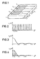
- FIG. 1 is shown a partial embodiment of the device of the invention given by way of example to make it better understand the operation.
- the device consists of the N single-mode guides 1 integrated in the common substrate 3, which has the form of a wafer, which forms the common electrode.
- the N metallizations 2 arranged on a part of the guides 1 allow the individual phase control of the wave transported by each of these guides. But we can also consider a conventional configuration of the electrodes; these being arranged two by two adjacent to each wave.
- the proposed device therefore comprises, in order to reconstitute the single large beam to be deflected, a certain number of elementary sources, to which a relative phase distribution is imposed such that each of the corresponding power increments arrives in phase on the plane at infinity the normal of which makes the desired angle 0 relative to that of the plane of the sources.
- the electrode control signals can respectively form the steps of a voltage ramp, which makes it possible to choose the angle 0 of deflection. But one can also choose a signal of precalculated shape to obtain a particular diffraction pattern.
- the angular distribution of intensity at infinity results from the composition of two terms: a distribution of network type comprising an indefinite series of regularly spaced network modes, as represented in FIG. 2, having undergone a convolution with the diffraction function of one of the elementary sources represented in FIG. 3.
- the propagation of the central mode but also that of a certain number of parasitic modes as represented in FIG. 4.
- the device of the invention is shown diagrammatically in FIG. 5.
- the source 4 of infrared radiation is coupled to the wafer 3 of electrooptical material, via a beam splitter 5 which can for example be produced in integrated optics.
- the signal generator 6 makes it possible to control the different electrodes 2 associated with each of the waveguides 1.
- the optical radiation which is coupled to the inputs of the waveguides thus makes it possible to obtain at the output the deflected beam 7.
- the second solution consists in making the waveguides 1 so as to vary the distance ⁇ along the wafer according to a predetermined random law ⁇ and ensuring that any pair of elementary sources is equidistant from the central source.
- ⁇ the coherent addition of intensity is entirely preserved only for a single direction 0.
- This modulation can also be introduced [ ⁇ ( ⁇ )] on the signals for controlling the electrodes equally each pair of symmetrical guides with respect to the central guide, the guides then being equidistant from each other. It can therefore be a random variation obtained by a generator of random signals of the known art superimposed on the initial ramp.
- a matrix of phase shifters can be obtained by stacking several devices described above. Such a matrix then makes it possible to carry out the scanning of the entire half-space situated beyond the plane of the outlet ends of the guides: we are then in the presence of a scanning device two-dimensional allowing an electronic order in site and deposit.
- a random modulation 100 (0) being equivalent to a modulation 106, this way of operating can facilitate the development of the phase shifter block whose pitch A can then be kept constant on the two dimensions.
- a set of auxiliary electrodes associated with each of the waveguides analogous to those of FIG. 1 and separated from it can be added to the device to facilitate the application of the voltage distribution corresponding to this random modulation.
- the device of the invention therefore allows random access to any point of the angular range scanned. This access can be very fast.
Landscapes
- Physics & Mathematics (AREA)
- Nonlinear Science (AREA)
- General Physics & Mathematics (AREA)
- Optics & Photonics (AREA)
- Optical Integrated Circuits (AREA)
Description
- La présente invention a pour objet un dispositif de déflexion d'un faisceau infra-rouge suivant une direction prédéterminée.
- Pour opérer la déflexion d'un faisceau d'énergie rayonnée avec une grande précision, il est, en général, préférable d'utiliser un dispositif fonctionnant par valeurs discrètes, celle-ci pouvant en effet être exactement définies par la structure même du dispositif; elles sont donc plus stables, c'est à dire insensibles aux fluctuations ou perturbations extérieures.
- Un réseau de diffraction permet une déflexion globale d'un faisceau incident suivant une direction privilégiée prédéterminée et suivant la direction qui lui est symétrique par rapport à la normale au plan du réseau. Un tel réseau ne permet donc d'obtenir la déflexion d'un faisceau incident que dans deux directions prédéfinies symétriques. Pour constituer un dispositif permettant de défléchir successivement un faisceau dans plusieurs directions définies, il est donc nécessaire d'associer plusieurs réseaux, avec les inconvénients que celà entraîne en ce qui concerne d'une part le rendement lumineux de la déflexion, et d'autre part, surtout, la précision de la déflexion.
- Un dispositif de l'art antérieur est décrit dans la demande de brevet français FR-A-2254057. Ce dispositif est un dispositif de déflexion d'un faisceau d'énergie rayonnée cohérente et polarisée, sous l'action d'un signal électrique de commande, comportant: une couche d'un matériau électro- optique; des électrodes de l'une des faces au moins étant transparentes, et des moyens d'excitation de ces électrodes recevant un signal de commande. L'une des faces de cette couche porte un ensemble d'électrodes de même étendue, contiguës mais isolées électriquement, portées sélectivement à des potentiels électriques de valeurs prédéfinies, modifiant ainsi spatialement le déphasage du faisceau incident afin de constituer les lignes d'un réseau diffractant. Le pas de ce réseau est variable et fonction de la répartition des valeurs prédéfinies du potentiel sur les électrodes.
- Contrairement à ce dispositif de l'art antérieur, le dispositif de l'invention concerne la déflexion d'un faisceau préalablement divisé en plusieur faisceaux élémentaires, chacun d'eux traversant respectivement un modulateur de phase comportant un guide d'onde et au moins une électrode qui lui est adjacente.
- De plus par rapport à ce dispositif de l'art antérieur, le dispositif de l'invention a pour objet la déflexion d'un faisceau situé dans le domaine infra-rouge. En effet l'extension du champ des possibilités dés dispositifs optoélectriques fonctionnant dans l'infra-rouge moyen, notamment ceux travaillant dans la bande 9,5 gm - 10,6 f.tm qui est celle dans laquelle fonctionne le laser à dioxyde de carbone, fait apparaître la nécessité d'utiliser un dispositif de déflexion rapide, donc statique, d'un faisceau lumineux permettant l'accès aléatoire de tous les points de l'intervalle angulaire de déflexion.
- L'invention a pour objet un dispositif de déflexion d'un faisceau infra-rouge comportant une source d'un faisceau infra-rouge et un corps en matériau électro-optique muni d'électrodes, des moyens générateur de signaux de commande reliés à ces électrodes, cette source étant couplée à ce corps, caractérisé en ce que ce corps comporte au moins une plaquette de matériau électro-optique et que ledit dispositif comprend des moyens de couplage et de division du faisceau infra-rouge en N faisceaux élémentaires, N étant un nombre entier déterminé, et N modulateurs de phase discrets disposés sur chaque plaquette, chaque modulateur de phase comportant un guide d'onde monomode auquel au moins une électrode est adjacente, chaque guide ayant une de ses extrémités couplée aux moyens de couplage et de division du faisceau infra-rouge et son autre extrémité formant une des N sources élémentaires qui délivrent un faisceau unique défléchi.
- D'autres aspects et avantages de l'invention seront mieux compris à l'aide de la description ci-après, fournie à titre d'exemple non limitatif, ainsi que des figures annexées parmi lesquelles:
- - la figure 1 représente le dispositif de l'invention.
- - la figures 2 à 4 illustrent différents aspects du dispositif de l'invention.
- - la figure 5 représente une vue schématique du dispositif de l'invention on.
- Le dispositif de l'invention est basé sur les possibilités de réalisation de guides d'ondes monomodes dans un substrat et de déphaseurs commandables utilisant l'effet électro-optique au sein d'un même matériau. On obtient ainsi de véritables circuits intégrés optiques regroupant sur une même plaquette plusieurs déphaseurs commandables individuellement. Le matériau de base utilisé est un diélectrique ou un semi-conducteur convenablement choisi. L'ensemble du dispositif est réalisé à la surface d'un substrat possédant des propriétés électrooptiques, tel que le niobate de lithium (LiNb03) et le tantalate de lithium (LiTa03) (pour le domaine visible ou infra-rouge proche), ou par exemple l'arseniure de gallium (AsGa) (pour l'infra-rouge proche et plus lointain). Dans un substrat de niobate de lithium par exemple, les guides d'ondes optique sont obtenus par diffusion de titane. Cette diffusion est sélective grâce à des procédés de photolithographie classique. Dans le cas de semi-conducteurs, ces guides d'ondes peuvent être réalisés grâce à des techniques d'épitaxie en phase liquide ou gazeuse. Ainsi les procédés convenant à l'élaboration de ces circuits intégrés optiques sont ceux qui sont utilisés dans la fabrication des dispositifs électroniques équivalents (épitaxie et/ou diffusion masquée, microlithographie par exemple). Il est donc possible en couplant une source de rayonnement infra-rouge aux extrémités d'entrée de ces guides d'ondes par l'intermédiaire d'un dispositif séparateur de faisceau, réalisé en optique intégrée par exemple, de réaliser le dispositif de l'invention tel qu'il apparaisse comme un réseau de N sources élémentaires (extrémités de sortie des N guides diffusés du circuit intégré optique) dont la phase relative est commandable de façon individuelle; N étant un nombre entier déterminé. Les électrodes sont disposées sur tout ou partie de chacun des guides diffusés et permettent ainsi d'en faire varier l'indice en fonction du champ électrique E appliqué.
- Le dispositif proposé se compose donc d'un réseau de N déphaseurs commandables intégrés à N guides dont les centres des extrémités, de sortie émergent de la plaquette substrat sur une ligne droite. La répartition des extrémités de sortie sur cette droite est symétrique par rapport à l'une d'entre elles.
- Dès lors, comme dans la théorie des réseaux de diffraction, si l'on effectue la composition en champ éloigné du rayonnement émis par les N sources on voit qu'à une direction particulière du plan perpendiculaire aux extrémités de sortie des N guides et passant par la droite lieu de leur centre correspond une répartition particulière des phases relatives de chacunes ou, ce qui revient au même, une répartition des tensions appliquées aux électrodes des déphaseurs. Il est donc possible, en modifiant la répartition de tension d'obtenir, dans un plan gisement par exemple, la déflexion du faisceau infra-rouge dans un certain domaine angulaire: le dispositif conforme à l'invention est donc un système de balayage électronique unidimensionnel appliqué au domaine optique.
- A la figure 1 est représentée une réalisation partielle du dispositif de l'invention donnée à titre d'exemple pour en faire mieux comprendre le fonctionnement. Le dispositif est constitué des N guides monomodes 1 intégrés dans le substrat commun 3, qui a la forme d'une plaquette, qui forme électrode commune. Les N métallisations 2 disposées sur une partie des guides 1 permettent la commande individuelle de phase de l'onde transportée par chacun de ces guides. Mais on peut aussi considérer une configuration classique des électrodes; celles-ci étant disposées deux par deux de façon adjacente à chaque d'onde.
- Le dispositif proposé comporte donc, pour reconstituer le faisceau unique de grande étendue à défléchir, un certain nombre de sources élémentaires, auxquelles on impose une distribution de phase relative telle que chacun des incréments de puissance corespondant arrive en phase sur le plan à l'infini dont la normale fait l'angle 0 désiré par rapport à celle du plan des sources.
- Les signaux de commande des électrodes peuvent respectivement former les paliers d'une rampe de tension, ce qui permet de choisir l'angle 0 de déflexion. Mais on peut aussi choisir un signal de forme précalculée pour obtenir une figure de diffraction particulière.
- De plus, si le pas A (distance entre deux sources élémentaires plus proches voisines) est maintenu constant comme représenté à la figure 1 la distribution angulaire d'intensité à l'infini résulte de la composition de deux termes: une distribution de type réseau comprenant une suite indéfinie de modes réseau régulièrement espacés, comme représenté à la figure 2, ayant subi une convolution avec la fonction diffraction de l'une des sources élémentaires représentée à la figure 3. Dans le cas général, on obtient donc non seulement la propagation du mode central, mais encore celle d'un certain nombre de modes parasites comme représenté à la figure 4.
- Ainsi le dispositif de l'invention est représenté schématiquement à la figure 5. La source 4 de rayonnement infra-rouge est couplée à la plaquette 3 de matériau électrooptique, via un séparateur de faisceau 5 qui peut être par exemple réalisé en optique intégrée. Le générateur de signaux 6 permet de commander les différentes électrodes 2 associées à chacun des guides d'onde 1. Les rayonnements optiques qui sont couplés aux entrées des guides d'ondes permettent ainsi d'obtenir en sortie le faisceau 7 défléchi.
- Deux solutions sont alors applicables pour supprimer le modes parasites:
- - La première solution consite à diminuer suffisamment la valeur de la distance A pour que le premier mode parasite tombe à l'extérieur du lobe de diffraction d'une des sources; la distance inter- mode est, en effet: A 0 = γ/Δ. Cette solution est la plus généralement appliquée en électromagnétisme mais présente dans le domaine des rayonnements infra-rouges l'inconvénient d'exiger un très grand nombre de sources.
- La deuxième solution consiste à réaliser les guides d'ondes 1 de manière à faire varier le long de la plaquette la distance Δ suivant une loi aléatoire εΔ prédéterminée et en assurant que toute paire de sources élémentaires est équidistante de la source centrale. On montre alors qu'à partir d'un nombre de sources N suffisamment élevé l'addition cohérente d'intensité n'est entièrement conservée que pour une seule direction 0. Cette modulation peut aussi être introduite [εØ(θ)] sur les signaux de commande des électrodes d'une manière égale chaque paire de guides symétriques par rapport au guide central, les guides étant alors équidistants les uns aux autres. Ce peut donc être une variation aléatoire obtenue par un générateur de signaux aléatoires de l'art connu superposée à la rampe initiale.
- A titre d'exemple, avec des guides d'ondes en arseniure de gallium et d'aluminium du type: Aix Ga1-x As à faible teneur en Aluminium, on peut considérer les ordres de grandeurs suivants:
- - N==91 à 101
- - Longueur d'intéraction de chaque guide déphaseur = 40 mm
- - Pertes par absorption dans les guides = 10%
- - Tension de commande = ± 50 V.
- - Lobes secondaires: -10 dB (max.) par rapport au lobe principal.
- Une matrice de déphaseurs peut être obtenue par empilement de plusieurs dispositifs décrits ci- dessus. Une telle matrice permet alors d'effectuer le balayage de tout le demi-espace situé au-delà du plan des extrémités de sortie des guides: on est alors en présence d'un dispositif de balayage bidimensionnel permettant une commande électronique en site et gisement. Une modulation aléatoire 100 (0) étant équivalente à une modulation 106, cette façon d'opérer peut faciliter l'élaboration du bloc de déphaseur dont le pas A peut alors être maintenu constant sur les deux dimensions.
- Un jeu d'électrodes auxiliaires associés à chacun des guides d'ondes analogues à celles de la figure 1 et séparées de celle-ci peut être ajouté au dispositif pour faciliter l'application de la répartition de tension correspondant à cette modulation aléatoire.
- Le dispositif de l'invention permet donc l'accès aléatoire en tout point du domaine angulaire balayé. Cet accès peut être très rapide.
- Le dispositif trouve en particulier son application dans les domaines suivants:
- - imagerie active;
- - dispositif de balayage et de prépointage rapide à accès aléatoire fonctionnant aussi bien à l'émission qu'à la réception;
- - dispositifs de pointage et poursuite ultra-rapide et/ou multicibles;
- - dispositifs de correction de fronts d'onde à commande électrique.
Claims (15)
Applications Claiming Priority (2)
| Application Number | Priority Date | Filing Date | Title |
|---|---|---|---|
| FR8309007A FR2547072B1 (fr) | 1983-05-31 | 1983-05-31 | Dispositif de deflexion d'un faisceau infra-rouge a commande electronique |
| FR8309007 | 1983-05-31 |
Publications (2)
| Publication Number | Publication Date |
|---|---|
| EP0130859A1 EP0130859A1 (fr) | 1985-01-09 |
| EP0130859B1 true EP0130859B1 (fr) | 1987-07-15 |
Family
ID=9289348
Family Applications (1)
| Application Number | Title | Priority Date | Filing Date |
|---|---|---|---|
| EP19840401027 Expired EP0130859B1 (fr) | 1983-05-31 | 1984-05-18 | Dispositif de déflexion d'un faisceau infra-rouge à commande électronique |
Country Status (3)
| Country | Link |
|---|---|
| EP (1) | EP0130859B1 (fr) |
| DE (1) | DE3464811D1 (fr) |
| FR (1) | FR2547072B1 (fr) |
Families Citing this family (2)
| Publication number | Priority date | Publication date | Assignee | Title |
|---|---|---|---|---|
| FR2611916B1 (fr) * | 1987-03-06 | 1989-05-26 | Thomson Csf | Systeme de recueil, par une station fixe, de donnees transmises par voie optique par n stations mobiles |
| IL121138A (en) * | 1997-06-23 | 2001-11-25 | Chiaro Networks Ltd | An integrated device for optical components for beam deflection |
Family Cites Families (4)
| Publication number | Priority date | Publication date | Assignee | Title |
|---|---|---|---|---|
| FR2254057A1 (en) * | 1973-11-27 | 1975-07-04 | Thomson Csf | Deflector for coherent polarised light - has transparent electrodes on liquid crystalline bed forming diffraction grating |
| US4013000A (en) * | 1975-11-20 | 1977-03-22 | Bell Telephone Laboratories, Incorporated | Optical crossbar switching network |
| US4386827A (en) * | 1980-10-27 | 1983-06-07 | Xerox Corporation | Electrooptical scanning device |
| US4439016A (en) * | 1981-11-06 | 1984-03-27 | Westinghouse Electric Corp. | Optical beam deflection system |
-
1983
- 1983-05-31 FR FR8309007A patent/FR2547072B1/fr not_active Expired
-
1984
- 1984-05-18 EP EP19840401027 patent/EP0130859B1/fr not_active Expired
- 1984-05-18 DE DE8484401027T patent/DE3464811D1/de not_active Expired
Also Published As
| Publication number | Publication date |
|---|---|
| FR2547072B1 (fr) | 1985-07-05 |
| DE3464811D1 (en) | 1987-08-20 |
| EP0130859A1 (fr) | 1985-01-09 |
| FR2547072A1 (fr) | 1984-12-07 |
Similar Documents
| Publication | Publication Date | Title |
|---|---|---|
| US20260036677A1 (en) | Modular three-dimensional optical sensing system | |
| JP2840593B2 (ja) | 電気光学的導波路デバイス | |
| US5239598A (en) | Electro-optic waveguide device | |
| US5623360A (en) | Time delay beam formation | |
| JPS61121007A (ja) | 光学的波長分割マルチプレキシング/デマルチプレキシングシステム | |
| EP3665744B1 (fr) | Dispositif de réception optique d'un signal provenant d'un réseau antennaire à commande de phase et système antennaire associé | |
| RU2200970C2 (ru) | Электрически перестраиваемый оптический фильтр | |
| EP0287444B1 (fr) | Dispositif de commande optique d'une antenne à balayage | |
| FR2743234A1 (fr) | Demultiplexeur de longueurs d'onde | |
| Dolfi et al. | Optically controlled true time delays for phased array antenna | |
| EP0130859B1 (fr) | Dispositif de déflexion d'un faisceau infra-rouge à commande électronique | |
| EP0048190B1 (fr) | Antenne réseau non dispersive, et son application à la réalisation d'une antenne à balayage électronique | |
| EP0642005B1 (fr) | Dispositif optique d'imagerie permettant l'analyse spectrale d'une scène | |
| Maák et al. | Realization of true-time delay lines based on acoustooptics | |
| EP3274766B1 (fr) | Source laser accordable en fréquence et procédé d'émission d'un faisceau laser accordable | |
| FR2880204A1 (fr) | Source laser a recombinaison coherente de faisceaux | |
| Tsai | RF Spectrum Analyzer | |
| Gesell et al. | True time delay beamforming | |
| Tsai | Integrated Acoustooptical Circuits for Real-Time Wideband Signal Processing | |
| Acoustooptics et al. | and Applications | |
| FR2635198A1 (fr) | Dispositif de commutation de faisceaux lumineux integre | |
| FR2881886A1 (fr) | Antenne multifaisceau de reception | |
| Xiao et al. | Photonic Microwave Signal Processing Based on Opto-VLSI Technology | |
| Juswardy et al. | Opto-VLSI-based broadband true-time delay generation for phased array beamforming | |
| Bélisle | Canactâ' |
Legal Events
| Date | Code | Title | Description |
|---|---|---|---|
| PUAI | Public reference made under article 153(3) epc to a published international application that has entered the european phase |
Free format text: ORIGINAL CODE: 0009012 |
|
| AK | Designated contracting states |
Designated state(s): DE GB SE |
|
| 17P | Request for examination filed |
Effective date: 19850320 |
|
| 17Q | First examination report despatched |
Effective date: 19860925 |
|
| GRAA | (expected) grant |
Free format text: ORIGINAL CODE: 0009210 |
|
| AK | Designated contracting states |
Kind code of ref document: B1 Designated state(s): DE GB |
|
| REF | Corresponds to: |
Ref document number: 3464811 Country of ref document: DE Date of ref document: 19870820 |
|
| PLBE | No opposition filed within time limit |
Free format text: ORIGINAL CODE: 0009261 |
|
| STAA | Information on the status of an ep patent application or granted ep patent |
Free format text: STATUS: NO OPPOSITION FILED WITHIN TIME LIMIT |
|
| 26N | No opposition filed | ||
| PGFP | Annual fee paid to national office [announced via postgrant information from national office to epo] |
Ref country code: GB Payment date: 19900423 Year of fee payment: 7 Ref country code: DE Payment date: 19900423 Year of fee payment: 7 |
|
| PG25 | Lapsed in a contracting state [announced via postgrant information from national office to epo] |
Ref country code: GB Effective date: 19910518 |
|
| GBPC | Gb: european patent ceased through non-payment of renewal fee | ||
| PG25 | Lapsed in a contracting state [announced via postgrant information from national office to epo] |
Ref country code: DE Effective date: 19920303 |