EP0130952A2 - Anordnung in ruhenden Umformern - Google Patents
Anordnung in ruhenden Umformern Download PDFInfo
- Publication number
- EP0130952A2 EP0130952A2 EP84850196A EP84850196A EP0130952A2 EP 0130952 A2 EP0130952 A2 EP 0130952A2 EP 84850196 A EP84850196 A EP 84850196A EP 84850196 A EP84850196 A EP 84850196A EP 0130952 A2 EP0130952 A2 EP 0130952A2
- Authority
- EP
- European Patent Office
- Prior art keywords
- transistor
- diode
- switching transistor
- current
- switching
- Prior art date
- Legal status (The legal status is an assumption and is not a legal conclusion. Google has not performed a legal analysis and makes no representation as to the accuracy of the status listed.)
- Withdrawn
Links
Images


Classifications
-
- H—ELECTRICITY
- H02—GENERATION; CONVERSION OR DISTRIBUTION OF ELECTRIC POWER
- H02M—APPARATUS FOR CONVERSION BETWEEN AC AND AC, BETWEEN AC AND DC, OR BETWEEN DC AND DC, AND FOR USE WITH MAINS OR SIMILAR POWER SUPPLY SYSTEMS; CONVERSION OF DC OR AC INPUT POWER INTO SURGE OUTPUT POWER; CONTROL OR REGULATION THEREOF
- H02M7/00—Conversion of AC power input into DC power output; Conversion of DC power input into AC power output
- H02M7/42—Conversion of DC power input into AC power output without possibility of reversal
- H02M7/44—Conversion of DC power input into AC power output without possibility of reversal by static converters
- H02M7/48—Conversion of DC power input into AC power output without possibility of reversal by static converters using discharge tubes with control electrode or semiconductor devices with control electrode
- H02M7/53—Conversion of DC power input into AC power output without possibility of reversal by static converters using discharge tubes with control electrode or semiconductor devices with control electrode using devices of a triode or transistor type requiring continuous application of a control signal
- H02M7/537—Conversion of DC power input into AC power output without possibility of reversal by static converters using discharge tubes with control electrode or semiconductor devices with control electrode using devices of a triode or transistor type requiring continuous application of a control signal using semiconductor devices only, e.g. single switched pulse inverters
- H02M7/5387—Conversion of DC power input into AC power output without possibility of reversal by static converters using discharge tubes with control electrode or semiconductor devices with control electrode using devices of a triode or transistor type requiring continuous application of a control signal using semiconductor devices only, e.g. single switched pulse inverters in a bridge configuration
Definitions
- the invention relates to an arrangement in a static converter, including at least one pair of mutually co-acting switching transistors, of which the first switching transistor is arranged to be controlled with a frequency exceeding the control frequency for the other switching transistor, and in which converter a diode is connected between the emitters and collectors of respective.transmitters.
- a Darlington circuit is well known for switching high power outputs.
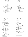
- the principal construction and operating mode of such a circuit is illustrated in Figure 1, and is characterized by high current amplification, because the effective current-amplification factor, calculated from the base of the transistor Tl to the collector of the transistor T2 is equal to the product of the current-amplification factors of both transistors.
- a Darlington circuit comprises a monolithic transistor, i.e. a transistor in which all components are formed on one and the same silicon plate.
- FIG. 2 An equivalent transistor circuit is illustrated in Figure 2, and it will be seen from the Figure that there is formed in the monolithic structure a parasite diode D l .
- this parasite diode is able to conduct the same current as the transistor, it has a relatively long reverse recovery time t , in the order of 1-10 ⁇ s, with respect to switching.
- the advantage with the parasite diode is that it can be used as a so-called free-wheel diode.
- a free-wheel diode is required when the Darlington transistor is used for switching the current to an inductive load.
- the modulation technique In order to function under these circumstances without serious losses occurring and without the provision df a current-limiting net, the modulation technique must be such that a transistor is without voltage when it is energized to its conductive mode, i.e. a Darlington transistor must be without voltage when it is energized, which limits the usefulness of the transistor.
- a well known modulation technique is pulse-width modulation (PWM), which requires the transistor to be energized to conductive mode with a full voltage between collector and emitter, which means, for example, that the free-wheel diode D2 will conduct when the Darlington transistor TR1 shown in Figure 3 is energized and brought to the conducting mode.
- PWM pulse-width modulation
- the base electrodes of the transistors are supplied with control signals which determine the frequency of the alternating voltage.
- a control voltage of high frequency is supplied to the input A to the first transistor TRl, TR3 and TR5 respectively, while a low frequency control voltage is supplied to the second transistor TR2, TR4 and TR6 respectively in each pair TR1, TR2 and TR3 respectively, i.e. the first transistor of each transistor pair will be switched on and off a number of times during the time when the second transistor of each transistor pair is throttled.
- Another knbwn method of emptying the inductance and reducing losses is to arrange a winding N2 in series with a diode D10, as indicated in Figure 6.
- a circuit D9-Zl will still be required, however, due to the leakage inductance between the windings, with resultant losses.
- FIG. 7 A preferred embodiment of a circuit according to the invention is illustrated in Figure 7. This circuit differs from the known circuit illustrated in Figure in that the inductance for limiting current growth is replaced with a transformer, which is coupled between the collector and emitter of the transistor TR2, across one, or optionally more, series-connected diodes Dll, enabling a feedback current (reverse recovery current I rr to be conducted.
- the transformer winding N1 forms the aforementioned separate voltage source.
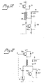
- FIGS 8 and 9 illustrate commutation from D2 to TR1. It is first assumed that the current I R flows through the free-wheel diode D2 to the line R, which constitutes one of the three phases of the motor M.
- Figures 10 and 11 illustrate commutation from TR1 to D2. It is assumed that the phase current I R flows from TR1 to the motor phase R, the lower part of the circuit illustrated in Figure 10 being without current. When TR1 is throttled, the current I R will commute to the free-wheel diode D2 ( Figure 11). Because of the inductance in the transformer winding N2, the current is forced to pass to the phase conductor R through the circuit Z1-D9. The voltage across this circuit Z1-D9 means that the transformer is saturated after a time period of where
- the phase current When the ferrite core is saturated, the phase current will flow via the coil or winding N2.
- the saturation time T there is obtained a power loss in the circuit Z1-D9, which with previously assumed values is about 7 watts. With previously assumed values, the saturation time T is about 4us.
- a further, small power loss is obtained at that moment when the transistor TR2 is blocked and thus becomes non-conducting. This power loss is illustrated in Figure 12.
- the phase current I R then flows through the coil or winding N2 and through TR2 from the phase R.
- the energy stored in the transformer is consumed in the circuit Z1-D9 is switched off, there is obtained a power loss which with the aforementioned toroid core and with other conditions unchanged will be less than 1 watt.
- the total power loss will be about 8 watts, which shall be compared with a power loss of 20 watts in an arrangement according to Figure 6.
- FIG 13 illustrates a simplified voltage source P in the form of a battery, which is coupled to D2 by means of a switch S and produces the reverse recovery current I rr , in order to rapidly discharge D2, as described above.
- the switch S which is shown in its closed position, may comprise, for example, a transistor or some other well known switch element, and the control is effective synchronously with the control of the first transistor TR1, and suitably the same control signal is supplied to the switch S as that supplied to the transistor TR1, as indicated in Figure 13.
- Another possibility of producing the reverse recovery current through the diode D2 is to discharge a capaciter through said diode.
Landscapes
- Engineering & Computer Science (AREA)
- Power Engineering (AREA)
- Inverter Devices (AREA)
- Analogue/Digital Conversion (AREA)
- Linear Motors (AREA)
- Lasers (AREA)
- Electronic Switches (AREA)
- Power Conversion In General (AREA)
Applications Claiming Priority (2)
| Application Number | Priority Date | Filing Date | Title |
|---|---|---|---|
| CH3680/83A CH653495A5 (fr) | 1983-07-05 | 1983-07-05 | Circuit de commande d'un convertisseur statique. |
| CH3680/83 | 1983-07-05 |
Publications (2)
| Publication Number | Publication Date |
|---|---|
| EP0130952A2 true EP0130952A2 (de) | 1985-01-09 |
| EP0130952A3 EP0130952A3 (de) | 1986-01-29 |
Family
ID=4261203
Family Applications (1)
| Application Number | Title | Priority Date | Filing Date |
|---|---|---|---|
| EP84850196A Withdrawn EP0130952A3 (de) | 1983-07-05 | 1984-06-20 | Anordnung in ruhenden Umformern |
Country Status (11)
| Country | Link |
|---|---|
| US (1) | US4570213A (de) |
| EP (1) | EP0130952A3 (de) |
| JP (1) | JPS6035967A (de) |
| AU (1) | AU3028784A (de) |
| BR (1) | BR8403127A (de) |
| CH (1) | CH653495A5 (de) |
| DK (1) | DK327884A (de) |
| ES (1) | ES533990A0 (de) |
| FI (1) | FI842698A7 (de) |
| NO (1) | NO842704L (de) |
| ZA (1) | ZA844178B (de) |
Cited By (1)
| Publication number | Priority date | Publication date | Assignee | Title |
|---|---|---|---|---|
| US6021055A (en) * | 1998-09-24 | 2000-02-01 | International Rectifier Corporation | Intentional cross conduction of converter circuit to ignite high ignition voltage loads |
Families Citing this family (4)
| Publication number | Priority date | Publication date | Assignee | Title |
|---|---|---|---|---|
| US4772810A (en) * | 1986-09-30 | 1988-09-20 | Hewlett-Packard Company | Apparatus for non-dissipative switching transistor snubber |
| FR2639489B1 (fr) * | 1988-11-22 | 1991-02-15 | Telemecanique | Dispositif interrupteur de puissance, notamment pour convertisseur de frequence |
| US5025360A (en) * | 1989-12-20 | 1991-06-18 | Sundstrand Corporation | Inverter switch with parallel free-wheel diodes |
| WO2006052032A1 (ja) * | 2004-11-15 | 2006-05-18 | Kabushiki Kaisha Toshiba | 電力変換装置 |
Family Cites Families (7)
| Publication number | Priority date | Publication date | Assignee | Title |
|---|---|---|---|---|
| US4245288A (en) * | 1978-10-31 | 1981-01-13 | Nasa | Elimination of current spikes in buck power converters |
| US4346309A (en) * | 1979-01-23 | 1982-08-24 | Westinghouse Brake And Signal Co., Ltd. | Controllable rectifier circuit |
| US4331994A (en) * | 1979-09-28 | 1982-05-25 | Borg-Warner Corporation | Shootthrough fault protection system for a voltage source transistor inverter |
| CA1151239A (en) * | 1980-09-25 | 1983-08-02 | Canadian Patents And Development Limited | Commutation circuits for thyristor inverters |
| US4358820A (en) * | 1980-12-29 | 1982-11-09 | United Technologies Corporation | Inverter with individual commutation circuit |
| US4376296A (en) * | 1981-03-02 | 1983-03-08 | Canadian Patents & Dev. Ltd. | DC-Side commutated inverter |
| US4414479A (en) * | 1981-07-14 | 1983-11-08 | General Electric Company | Low dissipation snubber for switching power transistors |
-
1983
- 1983-07-05 CH CH3680/83A patent/CH653495A5/fr not_active IP Right Cessation
-
1984
- 1984-06-04 ZA ZA844178A patent/ZA844178B/xx unknown
- 1984-06-20 EP EP84850196A patent/EP0130952A3/de not_active Withdrawn
- 1984-06-26 BR BR8403127A patent/BR8403127A/pt unknown
- 1984-07-03 US US06/627,694 patent/US4570213A/en not_active Expired - Fee Related
- 1984-07-04 AU AU30287/84A patent/AU3028784A/en not_active Abandoned
- 1984-07-04 NO NO842704A patent/NO842704L/no unknown
- 1984-07-04 FI FI842698A patent/FI842698A7/fi not_active Application Discontinuation
- 1984-07-04 DK DK327884A patent/DK327884A/da not_active Application Discontinuation
- 1984-07-04 ES ES533990A patent/ES533990A0/es active Granted
- 1984-07-05 JP JP59138107A patent/JPS6035967A/ja active Pending
Cited By (1)
| Publication number | Priority date | Publication date | Assignee | Title |
|---|---|---|---|---|
| US6021055A (en) * | 1998-09-24 | 2000-02-01 | International Rectifier Corporation | Intentional cross conduction of converter circuit to ignite high ignition voltage loads |
Also Published As
| Publication number | Publication date |
|---|---|
| BR8403127A (pt) | 1985-06-04 |
| FI842698L (fi) | 1985-01-06 |
| NO842704L (no) | 1985-01-07 |
| ZA844178B (en) | 1985-02-27 |
| DK327884D0 (da) | 1984-07-04 |
| FI842698A0 (fi) | 1984-07-04 |
| JPS6035967A (ja) | 1985-02-23 |
| ES8601591A1 (es) | 1985-10-16 |
| EP0130952A3 (de) | 1986-01-29 |
| FI842698A7 (fi) | 1985-01-06 |
| DK327884A (da) | 1985-01-06 |
| CH653495A5 (fr) | 1985-12-31 |
| AU3028784A (en) | 1985-01-10 |
| ES533990A0 (es) | 1985-10-16 |
| US4570213A (en) | 1986-02-11 |
Similar Documents
| Publication | Publication Date | Title |
|---|---|---|
| US5349157A (en) | Inverter power supply for welding | |
| US4007413A (en) | Converter utilizing leakage inductance to control energy flow and improve signal waveforms | |
| US4092709A (en) | Multiple output self oscillating converter regulator power supply | |
| EP0291120B1 (de) | Gesteuerte Hochfrequenzleistungsversorgung | |
| WO1991000643A1 (en) | Ac/dc conversion with reduced supply waveform distortion | |
| US4295083A (en) | Pulsed energy stepping motor power control unit | |
| US5014176A (en) | Switching converter with spike limiting circuit | |
| EP0079130B1 (de) | Verlustfreier Ausschalt-Entlastungskreis für mit Klemmdioden beschaltete Induktivlast | |
| US4760512A (en) | Circuit for reducing transistor stress and resetting the transformer core of a power converter | |
| EP0484610A1 (de) | Gleichstromschaltnetzteil mit geregelter Ausgangsspannung und Abtrennung zwischen Eingang und Ausgang | |
| WO1994018748A1 (en) | Control circuit for a switching dc-dc power converter including a controlled magnetic core flux resetting technique for output regulation | |
| US4093877A (en) | Semi-conductor switching circuit with transistor switching power loss reduction means | |
| US3963973A (en) | Nonsaturating asymmetric dc/dc converter | |
| US4308577A (en) | Base drive circuit | |
| EP0130952A2 (de) | Anordnung in ruhenden Umformern | |
| US4593204A (en) | Driver circuits for gate turn-off thyristors and bipolar transistors | |
| JP4083299B2 (ja) | ターンオフサイリスタを駆動する方法及び装置 | |
| US4605865A (en) | Input drive apparatus for power transistor | |
| US4393316A (en) | Transistor drive circuit | |
| GB2182815A (en) | Inductive load switching circuit | |
| US4015185A (en) | Semiconductor switching circuit with transistor switching power loss reduction means | |
| JPH02254969A (ja) | スイッチトモード電源回路 | |
| WO2000011784A1 (en) | A high voltage pulse generator using a non-linear capacitor | |
| JPH0221693B2 (de) | ||
| RU2139625C1 (ru) | Статический преобразователь с квазирезонансной коммутацией тока |
Legal Events
| Date | Code | Title | Description |
|---|---|---|---|
| PUAI | Public reference made under article 153(3) epc to a published international application that has entered the european phase |
Free format text: ORIGINAL CODE: 0009012 |
|
| AK | Designated contracting states |
Designated state(s): AT BE CH DE FR GB IT LI LU NL SE |
|
| PUAL | Search report despatched |
Free format text: ORIGINAL CODE: 0009013 |
|
| AK | Designated contracting states |
Designated state(s): AT BE CH DE FR GB IT LI LU NL SE |
|
| 17P | Request for examination filed |
Effective date: 19860204 |
|
| STAA | Information on the status of an ep patent application or granted ep patent |
Free format text: STATUS: THE APPLICATION HAS BEEN WITHDRAWN |
|
| 18W | Application withdrawn |
Withdrawal date: 19860610 |
|
| RIN1 | Information on inventor provided before grant (corrected) |
Inventor name: LJUNG, ERIK ANDERS |