EP0131048B1 - Circuit de mise en image a couplage de charge a faible bruit - Google Patents
Circuit de mise en image a couplage de charge a faible bruit Download PDFInfo
- Publication number
- EP0131048B1 EP0131048B1 EP84900592A EP84900592A EP0131048B1 EP 0131048 B1 EP0131048 B1 EP 0131048B1 EP 84900592 A EP84900592 A EP 84900592A EP 84900592 A EP84900592 A EP 84900592A EP 0131048 B1 EP0131048 B1 EP 0131048B1
- Authority
- EP
- European Patent Office
- Prior art keywords
- charge
- gate
- column
- ccd
- transfer device
- Prior art date
- Legal status (The legal status is an assumption and is not a legal conclusion. Google has not performed a legal analysis and makes no representation as to the accuracy of the status listed.)
- Expired
Links
- 230000010354 integration Effects 0.000 claims description 35
- 239000000758 substrate Substances 0.000 claims description 24
- 230000009467 reduction Effects 0.000 abstract description 15
- 238000010586 diagram Methods 0.000 description 38
- 238000009792 diffusion process Methods 0.000 description 33
- 230000005855 radiation Effects 0.000 description 30
- 230000000875 corresponding effect Effects 0.000 description 22
- 230000002596 correlated effect Effects 0.000 description 15
- 238000002347 injection Methods 0.000 description 14
- 239000007924 injection Substances 0.000 description 14
- 239000004065 semiconductor Substances 0.000 description 11
- 238000000034 method Methods 0.000 description 9
- 239000000969 carrier Substances 0.000 description 8
- 238000003860 storage Methods 0.000 description 8
- 239000003990 capacitor Substances 0.000 description 7
- 229910021420 polycrystalline silicon Inorganic materials 0.000 description 7
- 230000008569 process Effects 0.000 description 6
- 230000000694 effects Effects 0.000 description 4
- 230000008901 benefit Effects 0.000 description 3
- 230000001276 controlling effect Effects 0.000 description 3
- 230000005669 field effect Effects 0.000 description 3
- 230000015556 catabolic process Effects 0.000 description 2
- 239000002800 charge carrier Substances 0.000 description 2
- 238000006731 degradation reaction Methods 0.000 description 2
- 230000000593 degrading effect Effects 0.000 description 2
- 238000011067 equilibration Methods 0.000 description 2
- 238000004519 manufacturing process Methods 0.000 description 2
- 230000000737 periodic effect Effects 0.000 description 2
- 238000005036 potential barrier Methods 0.000 description 2
- 238000002360 preparation method Methods 0.000 description 2
- 239000000047 product Substances 0.000 description 2
- 238000009738 saturating Methods 0.000 description 2
- 239000000243 solution Substances 0.000 description 2
- 238000006467 substitution reaction Methods 0.000 description 2
- 230000003247 decreasing effect Effects 0.000 description 1
- 230000001934 delay Effects 0.000 description 1
- 230000003292 diminished effect Effects 0.000 description 1
- 230000004907 flux Effects 0.000 description 1
- 239000000463 material Substances 0.000 description 1
- 229920005591 polysilicon Polymers 0.000 description 1
- 238000012887 quadratic function Methods 0.000 description 1
- 238000009877 rendering Methods 0.000 description 1
- 230000004044 response Effects 0.000 description 1
- 229920006395 saturated elastomer Polymers 0.000 description 1
- 239000013589 supplement Substances 0.000 description 1
- 230000001360 synchronised effect Effects 0.000 description 1
Images





Classifications
-
- H—ELECTRICITY
- H10—SEMICONDUCTOR DEVICES; ELECTRIC SOLID-STATE DEVICES NOT OTHERWISE PROVIDED FOR
- H10F—INORGANIC SEMICONDUCTOR DEVICES SENSITIVE TO INFRARED RADIATION, LIGHT, ELECTROMAGNETIC RADIATION OF SHORTER WAVELENGTH OR CORPUSCULAR RADIATION
- H10F39/00—Integrated devices, or assemblies of multiple devices, comprising at least one element covered by group H10F30/00, e.g. radiation detectors comprising photodiode arrays
- H10F39/10—Integrated devices
- H10F39/12—Image sensors
- H10F39/15—Charge-coupled device [CCD] image sensors
- H10F39/153—Two-dimensional or three-dimensional array CCD image sensors
Definitions
- Charge coupled device imagers formed on a semiconductor substrate are described in Wolfe et al, The Infrared Handbook, Office of Naval Research, Department of the Navy, 1978, pp. 12-27 to 12-54. They typically comprise an array of parallel charge coupled device (CCD) serial registers receiving charge from adjacent photodetectors on the substrate.
- CCD charge coupled device
- the parallel CCD registers are arranged in vertical columns, all of their outputs being connected to a single horizontal CCD register which serves as the multiplexer. All of the column CCD registers are connected to a common input diffusion and a common input gate which separately introduces a FAT zero charge packet into each of the column CCD registers.
- This type of imager suffers from several inherent limitations. Specifically, electronic noise or jitter on the signals controlling the injection of the FAT zero charge packet from the input diffusion into each of the column registers causes the amount of FAT zero charge in each of the packets to vary, which in turn generates row correlated noise. Specifically, electronic jitter in the clock signals controlling the input diffusion and the adjacent overlying input gate electrodes-causes the capacity of each CCD bucket defining the amount of FAT zero charge to vary in synchronism with the jitter.
- thermal noise generated by the behavior of the semiconductor material.
- semiconductor surface states at the interface between the semiconductor substrate and the overlying dielectric layer causes the amount of charge carriers contained in each CCD bucket to vary, which in turn generates uncorrelated thermal noise in the video signal.
- N CCD The total amount of CCD noise from these two sources, N CCD , is equal to the square root of the sum of the squares of the row correlated noise, NFtc, and the thermal noise, N TH , in accordance with a well-known principle, which may be expressed as:
- each CCD bucket restricts the dynamic range of the imager. Specifically, an excessive amount of background radiation causes the photodetectors to generate so much charge as to saturate the charge carrying capacity of the CCD registers, thus causing the image to be washed out. Such an image can operate over only a very limited range of background radiation levels.
- One prior art solution to this problem was to interpose a gain control device between each photodetector and its corresponding column CCD register. Such a gain control device could be adjusted to limit the amount of charge generated by the photodetector for a given amount of incident radiation.
- the clocking speed of the vertical column CCD parallel registers is limited by the clocking speed of the horizontal multiplexing CCD register to which they are all connected.
- the clock frequency of the horizontal multiplexing register must be greater than the clocking frequency of the parallel vertical column registers by a factor proportional to the number of vertical columns in the array.
- the clock frequency of the horizontal multiplexing register is limited by the rise time of the CCD clock signal and the maximum speed the charge can be transferred, which places a fundamental limitation on the speed of such an imager.
- transfer noise sets a limit on the performance of these devices due to the large number of transfers required to reach the output.
- the dynamic range of a CCD imager is limited at extremely low background radiation intensities (such as those encountered in deep space) by the presence of thermal noise and row correlated noise. It is limited at very high background radiation intensities (such as those encountered on the ground in broad daylight) by the degradation of the signal-to-photon noise ratio caused by gain attenuation necessary to compensate for limited CCD charge capacity.
- the invention includes a low noise FAT zero injection circuit common to all column CCD registers where the entire CCD range can be exercised during setup and in which each FAT zero charge packet is metered by an overlying metering gate electrode of very small area in proportion to the depth of the surface potential well formed beneath the metering gate electrode during system operation. Reduction of the area of the metering gate electrode reduces fluctuations in the amount of charge stored beneath this electrode due to (1) electronic jitter in the applied voltage on the electrode and (2) surface state noise at the interface between the semiconductor substrate and the dielectric layer beneath the metering gate electrode.
- Noise is further reduced by the use of reference column subtraction in which the output signal from each CCD column register is subtracted from the output signal of a reference CCD column register having no photodetector input. This subtraction suppresses noise by common mode rejection.
- the outputs of a number of column CCD registers are further multiplexed by the use of a source follower common output circuit instead of the usual horizontal CCD multiplexing register. Substitution of a source follower circuit at the output of each CCD column register in place of the usual CCD multiplexing register facilitates the subtraction of each CCD column register output from the reference CCD column register output. It also removes the limitation in clocking frequency otherwise imposed by the horizontal CCD multiplexing register and eliminates transfer noise due to the horizontal CCD multiplexing register.
- Row correlated noise produced by electronic jitter in the applied voltage on the FAT zero metering gate, is reduced in proportion to the reduction in FAT zero metering gate area and in proportion to the common mode rejection ratio of the reference column subtraction feature.
- the reduction in thermal noise is also proportional to the reduction in FAT zero metering gate area.
- the invention also includes a bucket bailer feature in which very bright backgrounds may be suppressed without degrading the signal-to-photon noise ratio.
- the signal is proportional to the number No of photons impinging upon the photodetector.
- the photon noise is proportional to the square root of the number of photons, (NoP/2, so that the signal-to-noise ratio in the presence of high background radiation is roughly equal to
- Prior art background filters such as gain control circuits, which reduce either the number of photons, No, or photon-generated carriers, N o xquantum efficiency, necessarily reduce this signal-to-noise ratio.
- background radiation is suppressed to avoid saturating the CCD charge carrying capacity without reducing the signal generated by the photodetector.
- This unit cell circuit has the ability to periodically "bail" or remove a predetermined amount of charge from the storage well a selected number of times during each integration period before the integrated charge is transferred into the CCD column register as a charge packet.
- the frequency at which the storage well is thus bailed may be selected by the user to accommodate any level of background radiation so that the storage well and the CCD column register are not saturated regardless of the intensity of the photo current generated by the photodetector.
- the amount of charge bailed from the storage well is predetermined in accordance with voltages supplied to a set of bailing electrodes overlying an area on the substrate immediately adjacent the storage well.
- An individual CCD bailing circuit is associated with each photodetector in the CCD imager of this invention.
- row correlated noise and thermal noise (important at low background radiation levels) is reduced and signal-to-noise ratio (important at high background radiation levels) is increased in the present invention by the combination of the FAT zero metering gate area reduction, the reference column subtraction, and the CCD charge bailer features of this invention.
- the limitation imposed by CCD transfer noise on the speed of operation of the imager is preferably removed by the substitution of common source follower output circuits in place of the usual horizontal CCD multiplexing register. This latter feature, in addition to increasing the device speed, facilitates the reference row subtraction feature of the invention.
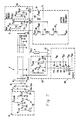
- the invention includes a semiconductive substrate (or "chip") 2 of N-type conductivity upon which a CCD imager is formed.
- the imager includes an array of photodetectors 4 arranged in columns and rows, each column of photodetectors 4 being associated with a CCD column serial register 6. If the CCD imager is a monolithic focal plane array, then each detector may comprise, for example, a P-type collection area formed in the surface of the N-type semiconductive substrate 2.
- Each photodetector generates positive charge carriers which are periodically integrated as a single charge packet during an integration period, the integrated packet then being injected into the adjacent CCD column serial register 6. Just as the next integration period begins, the charge packets previously injected into each column register 6 are transferred through the register 6 and into a multiplexer 8. The output signals from the parallel registers 6 are accessed by the multiplexers 8 associated with the parallel registers 6 into a source follower circuit 10 to form a serial train of signals.
- a FAT zero injector 12 injects a small amount of charge, commonly known as a FAT zero charge packet, into each column CCD register 6, once during each CCD clock cycle.
- the purpose is to enhance charge transfer efficiency.
- the amount of charge contained in each FAT zero charge packet is constant. Accordingly, the signal charge packets injected from each photodetector 4 into the corresponding column register 6 are simply added to the constant known amount of FAT zero charge.
- interface state noise or "surface state noise” described in Sequin et al, Charge Transfer Device, Academic Press, Inc., New York (1975), pp. 111-112.
- interface noise arises from a phenomena in which CCD charge packets held in the semiconductor substrate may randomly become trapped in crystalline surface states at the interface between the semiconductor substrate surface and the overlying insulating layer. This causes the amount of transferable charge to fluctuate. Such fluctuations give rise to interface state noise.
- electrical injection noise is caused by fluctuations or "jitter” in applied voltages controlling the operation of the charge coupled device.
- the capacity of an electrical potential "well” in a semiconductor substrate varies with fluctuations in the applied voltage on the overlying gate electrode forming the surface potential well. Such fluctuations create electrical injection noise.
- interface state noise and electrical injection noise are significant when the CCD imager views a scene having a low background radiation level.
- background photon noise arises from fluctuations in the background radiation level and is proportional to the square root of the number No of photons or photon generated carriers.
- the signal is directly proportional to the number No of photons or carriers, so that the signal-to-photon noise ratio is proportional to the square root of the number No of incident photons or photon-generated carriers.
- the problem is that if the detector gain is reduced in order to compensate for high background radiation levels, the number of photon generated carriers is necessarily reduced, which reduces the signal-to-photon noise ratio.
- the FAT zero injector 12 of Fig. 1 is illustrated in the schematic diagram of Fig. 2.
- the FAT zero injector 12 is formed on the semiconductive substrate 2 and includes a P-type input diffusion 20, connected to receive a clock signal ⁇ FZD , an insulated control gate 22 overlying the substrate 2 adjacent the diffusion 20 and connected to receive a control voltage V FZ1 , another insulated control gate 24 overlying the semiconductive substrate 2 adjacent the control gate 22 and connected to receive a control voltage V FZ2 , and a narrow insulated FAT zero metering gate 26 adjacent the control gate 24 overlying the substrate 2 and connected to receive a metering voltage V fz3 .
- the gates 22, 24 and 26 are preferably formed in a first layer of polycrystalline silicon on an insulating dielectric layer overlying the semiconductive substrate 2, in accordance with well-known techniques for fabrication of charge coupled devices.
- the injector 12 further includes a pair of screen gates 28, 30 overlying the gaps between the gate pairs 22, 24 and 24, 26, respectively, connected to receive a voltage V FZSCR .
- the screen gates 28, 30 are preferably formed in an upper level or second layer of insulated polycrystalline silicon in accordance with well-known techniques of charge coupled device fabrication.
- the CCD column register 6 Adjacent the FAT zero injector is the CCD column register 6 (typical of all column registers 6 illustrated in Fig. 1) which comprises a 4-phase, double level polysilicon charge coupled device of the type well-known in the art.
- the FAT zero gates 22, 24, 26, 28 and 30 and the input diffusion 20 are shared in common by all of the column CCD registers 6a, 6b, 6c, etc., of which Fig. 2 is a typical schematic diagram.
- the plural parallel column registers 6 are individually separated by parallel channel stops (not shown) formed in the surface of the substrate 2 in the well-known manner.
- a plurality of insulated gate electrodes 32 is formed in the lower level polycrystalline silicon layer while another plurality of insulating gate electrodes 34 is formed in the upper level of polycrystalline silicon, each upper level electrode 34 overlying the gap between the corresponding pair of adjacent lower level electrodes 32, as indicated in Fig. 2.
- These electrodes are connected in a sequential periodic progression to receive clock signals ⁇ 1 , ⁇ 2 , 0 3 , ⁇ 4 , as illustrated in Fig. 2, in accordance with well-known 4-phase CCD clocking principles.
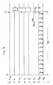
- the clock signals ⁇ FZD ⁇ 1 , ⁇ 2 , ⁇ 3 , and ⁇ 4 are illustrated in Figs. 4b, c, d, e and f, respectively, and will be discussed in detail later in this specification.
- the clock signal ⁇ FZD causes the FAT zero injector 12 to inject a single FAT zero charge packet into the CCD column register 6.
- Fig. 5a corresponds to that portion of Fig. 2 illustrating the FAT zero injector 12.
- Operation of the FAT zero injector 12 begins when the clock signal ⁇ FZD is temporarily pulsed positively, raising the surface potential of the diffusion 20 to the dashed-line level illustrated in Fig. 5b. This causes positive charge or "holes" to be injected from the diffusion 20, beneath the control gate 22 and into the surface potential well beneath the gate 24 illustrated in solid-line in Fig. 5b. Thereafter, the clock signal ⁇ FZD returns to its ambient level so that the surface potential in the diffusion 20 returns to the solid-line level illustrated in Fig. 5b.
- the charge Q FZ stored beneath the control gate 24 fills the surface potential well beneath the gate 24 to the top defined by the surface potential barrier beneath the gate 22, any excess charge being withdrawn into the input diffusion 20.
- the clocksignals ⁇ 3 and ⁇ 4 applied to the CCD gates 34a, 32a, respectively are pulsed downwardly in potential, thus causing the surface potential beneath them to assume the dashed-line configuration illustrated in Fig. 5b.
- the charge packet Q FZ is transferred as a FAT zero charge packet beneath the gate 34a to be stored in the surface potential well formed beneath the gate 32a.
- the FAT zero charge packet is then transferred through the CCD column serial register 6 in accordance with well-known principles of CCD charge transfer.
- the amount of charge Q Fz contained in the FAT zero packet is determined by the difference in the voltages V FZ1 and V FZ2 , which fluctuates due to the presence of electrical injection noise on the gates 22 and 24.
- Such fluctuations cause the FAT zero charge to fluctuate synchronously in all CCD serial column registers 6 in the array of Fig. 1.
- These fluctuations cause row correlated noise because the gates 22 and 24 are shared in common among all of the CCD serial registers 6, as is the input diffusion 20.
- the amount of charge contained in the FAT zero charge packet Q FZ also varies due to interface state noise beneath the gates 24 and 26. Such interface state noise is uncorrelated but does cause the amount of charge in the FAT zero charge packet Q Fz to fluctuate. All fluctuations, both interface state noise and electrical injection noise, induce noise into the video output signal generated by the CCD imager of Fig. 1.
- the effects of electrical injection noise and interface state noise are suppressed by the use of the FAT zero metering gate 26 of reduced area.
- the device illustrated in Fig. 5a may be operated in the low noise mode illustrated in Fig. 5c, in which the FAT zero charge packet Q' FZ illustrated in Fig. 5c is stored in the narrow surface potential well beneath the equally narrow FAT zero metering gate 26.
- the voltages V FZ1 and V FZ2 are set to be equal to one another so that the gates 22 and 24 perform the same charge equilibration function, while the voltage V FZ3 is set to be more negative than the latter.
- the width W1 of the control gate 24 is of the order of 45 microns while the width W2 of the metering gate 26 is of the order of only 6 microns.
- Fig. 8 illustrates in plan view another (preferred) technique of using a channel stop 200 to reduce the effective area of the control gate 26 by a factor of ten by constructing the width of the charge flow channel 202 beneath the gate 24.
- This relative reduction in area of the metering gate 26 reduces the fluctuation in the amount of charge Q' FZ of the FAT zero charge packet stored beneath the metering gate 26 caused by electrical injection noise in the voltages V FZ2 and V FZ3 or surface state noise at the semiconductor-dielectric interface beneath the gate 26.
- the effect of interface state noise on the amount of charge stored beneath the metering gate 26 is reduced because reduction in the area of the metering gate 26 reduces the ratio of the number of interface states beneath the metering gate 26 to the number of carriers in the FAT zero charge packet Q' Fz .
- the effect of electrical injection noise on the amount of charge stored beneath the metering gate 26 is reduced because the charge storing capacity of the surface potential well beneath the metering gate 26, illustrated in Fig. 5c, changes proportionately less with fluctuations in the applied voltages on the metering gate 26.
- Row correlated noise is further reduced by the use of reference column subtraction, illustrated in Fig. 1.
- the serial succession of charge packets in each column register 6 generates output signals in each source follower 10, which are multiplexed on a column-by-column basis by each multiplexer 8 operating in synchronous succession with one another.
- the output from each source follower 10 is connected to the input of a sample-and-hold subtractor 42, with the exception of the first or left-most column register 6a in Fig. 2, its source follower being connected instead to a separate sample-and-hold subtractor 44.
- the outputs from the sample-and-hold subtractors 42, 44 are connected to the positive and negative inputs of a differential amplifier 46, respectively.
- the reference sample-and-hold subtractor 44 samples and holds each output signal from the reference column register 6a, while the sample-and-hold subtractor 42 samples and holds, in turn, each output signal from the remaining CCD column registers 6b, 6c, etc., as it is multiplexed by the corresponding multiplexer 8.
- each output signal from each of the remaining CCD column registers 6b, 6c, etc. is subtracted in turn from the output signal of the reference CCD column 6a at the differential amplifier 46.
- the column of photodetectors 4 associated with the reference CCD column register 6a are prevented from injecting charge, in a manner to be described later in this specification.
- the reference CCD column register 6a contains only the FAT zero charge packets with associated row correlated noise and uncorrelated interface state noise. Because the row correlated noise is the same from column to column, the subtraction performed by the differential amplifier 46 common mode rejects the row correlated noise, producing a video signal at the differential amplifier output 46a in which row correlated noise is suppressed in proportion to the common mode rejection ratio achieved by the subtraction performed by the differential amplifier 46.
- the schematic diagram of Fig. 2 is typical of all the CCD column registers 6a, 6b, 6c, etc., illustrated in Fig. 1, each component therein also being typical.
- the multiplexer 8 includes an output diffusion 50, a multiplexing gate 52, a multiplexing transistor 54, comprising a P-channel field effect transistor, and a screen gate 56.
- P-channel field effect transistor refers to a P-type conductivity source and drain formed in the substrate 2 and an insulated polycrystalline silicon gate electrode overlying the transistor's source-to-drain channel.
- the source of the transistor 54 is connected to receive a clock signal ⁇ TO while its drain is connected to the CCD gate 52.
- the gate of the transistor 54 is connected to receive a clock signal ⁇ REn , where the index n corresponds to the number of the particular column in which the register 6 is located.
- the clock signal RE n initiates the transfer of each charge packet from beneath the last electrodes 32c, 34c of the column CCD register 6, underneath the multiplexing gate 52 and the screen gate 56 and into the output diffusion 50.
- the source follower circuit 10 senses the magnitude of the charge packet received in the output diffusion 50. It comprises a source transistor 60, a source follower transistor 62, a drain transistor 64 and a storage capacitor 66. Each of the transistors 60, 62, 64 comprise P-channel field effect transistors.
- the source of the transistor 60 is connected to a voltage supply V sso , its gate being connected to a voltage supply V GG0 and its drain connected to the source of the source follower transistor 62 and to the output node O " .
- the gate of the source follower transistor 62 is connected to the output diffusion 50 while its drain is connected to the source of the transistor 64.
- the gate of the transistor 64 is connected to receive the clock signal RE n while its drain is connected to the voltage supply V DDO .
- One electrode of the capacitor 66 is connected to the gate of the source follower transistor 62 while its other electrode is connected to the substrate voltage V sua .
- the capacitor 66 functions to supplement the charge storing capacity of the source follower transistor gate. Each charge packet entering the output diffusion 50 under control of the multiplexer 8 is stored on the capacitor 66 and increases the voltage on the gate of the source follower transistor 62, thus raising the voltage on the output node O n .
- the advantage of the source follower circuit 10 is that it facilitates the reference column subtraction function illustrated in Fig. 1 and eliminates the clock speed limitations previously imposed by the use of a prior art horizontal CCD multiplexing register, which the source follower circuits 10 replace.
- a source follower reset circuit 10a resets the charge and voltage of the output diffusion 50 and includes a screen gate 70, a CCD gate 72 and a drain diffusion 74.
- the screen gate 70 is connected to receive the voltage V SCR2
- the CCD gate 72 is connected to receive the clock signal ⁇ RSO
- the drain diffusion 74 is connected to receive the voltage V Rso .
- the clock signal ⁇ RSO is operated in synchronism with the CCD clock signals ⁇ 1 , ⁇ 2 , ⁇ 3 , ⁇ 4 to reset the output diffusion 50 once every CCD clock cycle.
- Fig. 2 illustrates only one photodetector 4 associated with the column register 6, it being understood that there is a column of many photodetectors as illustrated in Fig. 1.
- photo-generated carriers from the photodetector 4 are injected into the CCD register 6 beneath CCD gate 32b through a CCD channel 82 comprising a diffusion 92, a control gate 84, a screen gate 86, an integration gate 88 and a transfer gate 90.
- the photodetector 4 is connected to a common bias voltage supply V DET .
- the control gate 84 is connected to a voltage supply V GG
- the screen gate 86 is connected to a voltage supply V SCR
- the integration gate 88 is connected to receive a clock signal ⁇ ST
- the transfer gate 90 is connected to receive the clock signal ⁇ Tl .
- the transfer gate 90 partially overlies the integration gate 88 and the CCD gate 32b as illustrated in the simplified diagram of Fig. 6a.
- Photocarriers generated by the photodetector 4 flow beneath the gates 84 and 86 and are accumulated or "integrated" beneath the integration gate 88 in a surface potential well formed in the substrate 2 during an integration period T,.
- clock signal ⁇ Tl is pulsed negatively while the clock signal ⁇ ST is pulsed positively.
- This ejects the integrated charge from beneath the gate 88 and under the transfer gate 90 into the CCD column register 6 beneath the CCD gate 32b.
- This operation is illustrated in Figs. 3a and 3b, showing the periodic movement of the clock signals ⁇ Tl and ⁇ ST at the end of each integration period T,.
- the amount of charge contained in each charge packet is a measure of the video signal amplitude generated by the photodetector 4.
- a significant problem is that, in the presence of high background radiation levels, the amount of photocarriers generated by the photodetector 4 may far exceed the charge storage capacity of the surface potential well formed beneath the control gate 88 or of the surface potential wells formed in the column CCD register 6 beneath the various CCD gates 32, 34. If this capacity is so exceeded, the video signal may be distorted or completely lost.
- Prior art attempts to avoid this problem by reducing the gain of the photodetector 4 created another problem by reducing the signal-to-photon noise ratio, as previously described.
- the novel CCD charge bailer 80 shown in Fig. 2 comprising control gates 100,102,104, drain diffusion 106 and screen gates 108, 110 and 112.
- An individual bucket bailer 80 is associated with each one of the plurality of photodetectors 4 in the array of Fig. 1.
- the screen gates 108, 110, 112 are connected to the screen gate voltage supply V SCR .
- the control gate 100 is connected to receive the clock signal V B1
- the control gate 102 is connected to receive the clock signal V 82
- the control gate 104 is connected to a DC voltage supply V B3 while the drain diffusion 106 is connected to a drain voltage supply Vp R .
- Fig. 6a is an enlarged schematic diagram of the bucket bailer 80 corresponding to Fig. 2 and Fig. 6b is a diagram illustrating the electrical substrate surface potential corresponding to the schematic diagram of Fig. 6a.
- the clock signals ⁇ Tl , V B1 and V B2 are relatively high in voltage while the clock signal ⁇ ST is relatively low in voltage, so that the surface potential assumes the solid-line configuration illustrated in Fig. 6b.
- the surface potential well beneath the gate 88 is progressively filled by photocarriers generated in the photodetector 4.
- the clock signals V B1 and V B2 are periodically pulsed negatively so that the surface potential beneath the control gates 100, 102 drops to the dashed-line level illustrated in Fig. 6b, forming a surface potential well therebeneath. Thereafter, the clock signals V B1 and V B2 return to their original positive levels, causing the surface potential beneath the gates 100, 102 to return to the solid-line configuration illustrated in Fig. 6b. This causes a fractional amount, Q BAIL , of the charge held beneath the integration gate 88 to be diverted beneath the gate 102. This charge is dumped over the surface potential barrier beneath the gate 104 into the drain diffusion 106. The charge Q BAIL , is the charge "bailed" from beneath the gate 88.
- the frequency f BAIL of the bail clock signals V B1 and V B2 may be increased to accommodate an increased background radiation level. It is contemplated that an intelligent device 120 (Fig. 1) may be used to control the frequency f BAIL of the clock signals V B1 and VB 2 in response to variations in the background radiation level.
- the bailed charge Q BAIL is a constant which is determined by the difference in magnitude of the clock signals V B1 and V B2 .
- the charge Q TOTAL generated by the photodetector 4 during the integration period T is equal to the charge Q CCD dumped from beneath the integration gate 88 into the CCD column register 6 at the end of the integration period T, plus the product of the bailed charge Q BAIL , the integration period T, and the bail frequency F BAIL , This may be expressed as:
- a significant advantage of the CCD bailer 80 is that the bail frequency F BAIL may be adjusted to accommodate any background radiation level without degrading the signal-to-photon noise ratio because the photo-generated current from the detector 4 is not diminished in this invention. Accordingly, the CCD imager of this invention is useful for viewing very dim signals in the presence of very low background radiation, such as that encountered in deep space, and also for viewing images in the presence of very bright background radiation, such as that encountered in bright daylight on the ground. It is believed that this is the first such CCD imager having such wide versatility.
- Fig. 7 is a graph illustrating the performance of the charge bailer of this invention (dashed-line) compared with the performance of prior art imagers (solid-line).
- the ordinant of the graph of Fig. 7 corresponds to the relative imager responsivity plotted logarithmically while the abscissa of the graph of Fig. 7 corresponds to the background radiation level, also plotted logarithmically. Note how fast the responsivity of the prior art imager falls off with increase in background radiation level (solid-line) while the relative responsivity of the CCD imager of this invention using CCD charge bailing hardly falls off at all (dashed-line).
- FIG. 7 Detailed description of reference column subtraction
- the first column register 6a is used to provide the reference signal which is subtracted from the output signals from the other column registers 6b, 6c, etc.
- the output voltage from the sample-and-hold subtractor 44 (associated with the reference column register 6a) is applied to the negative input of the differential amplifier 46.
- the output voltage from the sample-and-hold subtractor 42 is applied to the positive input of the differential amplifier 46.
- the transfer gates 90 associated with the first or left-most reference CCD column register 6a (only) of Fig. 1 are not connected to receive the clock signal ⁇ Tl , contrary to the schematic diagram of Fig. 2, but are instead connected to a sufficiently high voltage source to block charge flow beneath the transfer gate 90.
- the transfer gates associated with the remaining column registers 6b, 6c, etc., of Fig. 1 are each connected as illustrated in Fig. 2 to permit charge to flow from the corresponding photodetectors.
- the reference signal derived from the reference column register 6a is applied to the negative input of the differential amplifier 46 and represents FAT zero charge and noise only.
- the reference signal is subtracted from the output signals of the other column registers 6b, 6c, etc., in the differential amplifier 46 to eliminate any row correlated noise in the manner previously described in this specification.
- Fig. 4 includes diagrams of the time domain waveform of the clock signals RE1 through RE15 (Fig. 4a), ⁇ FZD (Fig. 4b), ⁇ 1 through ⁇ 4 (Figs. 4c through 4f), ⁇ Tl (Fi g. 4 g ), ⁇ RSO (Fig. 4h), and ⁇ TO (Fig. 4i).
- Fig. 3 illustrates the overall operation during the integration period T,.
- Fig. 4 illustrates the detailed operation during the multiplexing period T MUX which is repeated many times over the integration period T, of Fig. 3.
- Fig. 4 has a scale much larger than that of Fig. 3.
- the integration T, period begins at time to of Fig. 3 when the clock signals ⁇ Tl , V B1 and V B2 are held at a positive voltage while the clock signal ⁇ ST is held at a lesser voltage to create a surface potential well beneath the integration electrode 88 illustrated in solid line in Fig. 6b. Immediately, photo-generated carriers from the photodetector 4 flow beneath and are accumulated under the electrode 88. This occurs simultaneously in the case of all of the photodetectors 4 in the CCD imager of Fig. 1.
- Each source follower circuit 10 immediately senses a new charge packet and then each of the fifteen source follower circuits 10 associated with each of the fifteen column registers 6 is successively multiplexed (or sampled) one at a time. This process is repeated forty-five times (during forty-five successive multiplexing periods T MUX ) until all the previously injected charge packets have been multiplexed through the source followers 10.
- the first multiplexing period T MUX (1) begins at time t A .
- the clock signal RE1 is pulsed negatively, which activates the multiplexer 8 and source follower 10 of the first column register 6a of the CCD imager of Fig. 1.
- clock signal RE1 turns the multiplexing transistor 54 of column register 6a "on", thus applying the relatively low voltage clock signal ⁇ TO to the multiplexing electrode 52 of the column register 6a. This creates an attractive surface potential well beneath the multiplexing gate 52, causing a charge packet previously stored beneath the CCD gate 32c of the column register 6a to be transferred and stored beneath the multiplexing gate 52.
- the clock signal ⁇ TO is pulsed positively, causing the charge packet stored beneath the multiplexing gate 52 to be transferred into the output diffusion 50 of the column register 6a.
- the charge packet is stored in the combined capacitance of the diffusion 50, the capacitor 66 and the gate of the source follower transistor 62.
- the charge packet stored on the capacitor 66 increases the gate voltage of the source follower transistor 62, thus decreasing its source-to-drain current and raising the voltage on the output node 0 1 of the column register 6a. This increase in voltage is proportional to the size of the charge packet transferred beneath the multiplexing electrode 52 at time t B .
- the voltage on the output node 0 1 is immediately subtracted in a sample-and-hold subtractor 44 from the voltage previously present on that output node to generate an output voltage V OUTPUT (1 ) representative of the absolute size of the charge packet sensed in the output diffusion 50 at time t B .
- the output voltage V OUTPUT (1) is applied by the sample-and-hold subtractor 44 to the negative input of the differential amplifier 46.
- the sample-and-hold subtractor 44 applies this output voltage throughout the remainder of the multiplexing period T MUX .
- the clock signal RE1 is turned "off", or returned to its higher ambient level.
- the clock signal RE2 is pulsed negatively, which activates the multiplexer 8 and source follower 10 associated with the second CCD column register 6b.
- the same operation as described in connection with the first column register 6a then takes place in the second column register 6b of Fig. 1.
- the clock signal ⁇ TO is again pulsed positively, and a voltage is generated at the output node 0 2 of the second column register 6b, representative of the signal charge packet sensed at the source follower 10 of the column register 6b.
- This voltage is subtracted in the sample-and-hold subtractor 42 from the voltage previously present on the output node O2 to generate an output voltage V OUTPUT (2) representative of the sensed signal charge packet at the output node 0 2 .
- This output voltage is applied to the positive input of the differential amplifier 46.
- the differential amplifier 46 in turn, generates an output voltage V OUTPUT (2) ⁇ V OUTPUT (1).
- the remaining 44 charge packets stored in each of the fifteen column registers 6 are then transferred down by one more CCD unit cell in accordance with the following description of operation.
- the alternate pairs of those adjacent CCD gates 32, 34 which are connected (in Fig. 2) to receive the clock signals ⁇ 1 , ⁇ 2 , respectively, are called the " ⁇ 1 , ⁇ 2 gates”.
- the remaining pairs of those adjacent CCD gates 32, 34 which are connected to receive the clock signals ⁇ 3 , ⁇ 4 , respectively, are called the " ⁇ 3 , ⁇ 4 gates”.
- the clock signals ⁇ 1 , 02 are pulsed negatively while the clock signals ⁇ 3 , 04 are pulsed positively, causing all the charge packets to be transferred out from under the ⁇ 3 , ⁇ 4 gates and to be stored beneath the next succeeed- ing ⁇ 1 , ⁇ 2 gates.
- all charge packets in the 15 column registers 6 are simultaneously moved downward toward the source follower 10 by a distance corresponding to one CCD unit cell. This concludes the first multiplexing period T MUX (1).
- a new charge packet is now stored beneath each of the output gates 32c of the fifteen column registers 6 in preparation for the next multiplexing cycle time T mux (2).
- the multiplexing process previously described in connection with the multiplexing time T MUX (1) is repeated during successive multiplexing periods T Mux (2) through T Mux ⁇ 45) so that all the charge packets output from the forty-five detectors associated with each of the fifteen column registers 6 are multiplexed through the corresponding source followers 10 in each of the fifteen column registers 6.
- the clock signal ⁇ Tl is pulsed negatively which permits charge flow beneath the transfer gate 90. This occurs only at the end of the multiplexing time period T Mux (45) but not at any of the other multiplexing time periods T MUX (1) through T Mux (44).
- the clock signal ⁇ ST is pulsed positively, causing the photo-generated charge packets accumulated beneath the integration gates 88 throughout the array of Fig. 1 to be injected under the respective transfer gates 90 into the CCD column registers 6, in the manner previously described in connection with Fig. 2. This concludes the integration period T, for all detectors 4 in the CCD imager of Fig. 1.
- the clock signal ⁇ Tl is turned “off” and at time t s , the clock signal ⁇ ST is turned “off", thus beginning the next integration period T, for all photodetectors 4 throughout the imager of Fig. 1.
- the clock signal ⁇ RSO is pulsed negatively, which activates the source follower reset circuit 10a. Specifically, the output diffusion 50 is reset to the voltage V R of the drain diffusion 74 at time t 6 by virtue of the negative voltage applied at this time by the clock signal ⁇ RSO to the gate 72, rendering the channel between the output diffusion 50 and the drain diffusion 74 conductive.
- the output node comprising the output diffusion 50, the capacitor 10 and the gate of the source follower transistor 62 is reset in preparation for receipt of the next charge packet in the diffusion 50.
- this process may be performed not only at time t 6 but also at time t' of Fig. 4h.
- the bucket bailer 80 operates periodically to bail a set amount of charge Q BAIL out of the surface potential well beneath the integration gate 88.
- the frequency f BAIL at which the CCD bailer 80 is operated is preferably adjusted to precisely compensate for excessive background radiation flux so as to avoid overfilling the surface potential well beneath the integrating gate 88. This adjustment may be performed by an intelligent device 100, which responds to changes in background radiation level, illustrated in Fig. 1.
- the period T RE of each of the clock signals RE1 through RE15 must be at least on the order of 16 microseconds, corresponding to the maximum slew rate noise limit of each of the source follower circuits 10.
- the duration of the multiplexing time period T MUX must be at least as great as the product of the time period T RE multiplied by the number of column registers 6 in the CCD imager plus 2 additional intervals T RE to allow for multiplexing delays.
- T Mux equals 16 microseconds times 17 or about 272 microseconds.
- the integration time period T is about equal to the multiplexing time period T MUX multiplied by the number of detectors per column.
- T equals 272 microseconds times 45 or about 12 milliseconds.
- the number of detectors per column and the number of columns per array thus determines the duration of the time periods T MUX and T, and may be chosen by the user to conform to the specifications of the system in which the invention is to be used.
Landscapes
- Solid State Image Pick-Up Elements (AREA)
- Transforming Light Signals Into Electric Signals (AREA)
Abstract
Claims (4)
Applications Claiming Priority (2)
| Application Number | Priority Date | Filing Date | Title |
|---|---|---|---|
| US458607 | 1983-01-17 | ||
| US06/458,607 US4523326A (en) | 1983-01-17 | 1983-01-17 | Low noise charge coupled imager circuit |
Publications (2)
| Publication Number | Publication Date |
|---|---|
| EP0131048A1 EP0131048A1 (fr) | 1985-01-16 |
| EP0131048B1 true EP0131048B1 (fr) | 1987-03-18 |
Family
ID=23821435
Family Applications (1)
| Application Number | Title | Priority Date | Filing Date |
|---|---|---|---|
| EP84900592A Expired EP0131048B1 (fr) | 1983-01-17 | 1983-12-30 | Circuit de mise en image a couplage de charge a faible bruit |
Country Status (4)
| Country | Link |
|---|---|
| US (1) | US4523326A (fr) |
| EP (1) | EP0131048B1 (fr) |
| JP (1) | JPS60500396A (fr) |
| WO (1) | WO1984003017A1 (fr) |
Families Citing this family (9)
| Publication number | Priority date | Publication date | Assignee | Title |
|---|---|---|---|---|
| US4733077A (en) * | 1984-12-20 | 1988-03-22 | Hughes Aircraft Company | Noise immune infrared readout circuitry |
| US4743762A (en) * | 1984-12-20 | 1988-05-10 | Hughes Aircraft Company | Noise immune infrared readout circuitry and technique |
| US4866496A (en) * | 1986-06-24 | 1989-09-12 | U.S. Philips Corp. | Charger transfer device (CTD), eliminating the background level of a detected signal, detection structure and method of using such a CTD |
| JP2586727B2 (ja) * | 1990-11-09 | 1997-03-05 | 三菱電機株式会社 | 電荷検出回路の制御装置 |
| JP3834841B2 (ja) * | 1995-08-03 | 2006-10-18 | 株式会社日立製作所 | 固体撮像素子 |
| US6101294A (en) * | 1997-06-02 | 2000-08-08 | Sarnoff Corporation | Extended dynamic imaging system and method |
| JP3879987B2 (ja) * | 2002-04-10 | 2007-02-14 | 日本ビクター株式会社 | 撮像装置 |
| US20050203427A1 (en) * | 2004-03-15 | 2005-09-15 | Impedance Vascular Imaging Products, Llc | Stenosis detection device |
| US20080050201A1 (en) * | 2006-08-25 | 2008-02-28 | Valade Franklin H | Anti-theft tack |
Family Cites Families (9)
| Publication number | Priority date | Publication date | Assignee | Title |
|---|---|---|---|---|
| US3683193A (en) * | 1970-10-26 | 1972-08-08 | Rca Corp | Bucket brigade scanning of sensor array |
| US3925657A (en) * | 1974-06-21 | 1975-12-09 | Rca Corp | Introduction of bias charge into a charge coupled image sensor |
| US3931463A (en) * | 1974-07-23 | 1976-01-06 | Rca Corporation | Scene brightness compensation system with charge transfer imager |
| US4010319A (en) * | 1975-11-20 | 1977-03-01 | Rca Corporation | Smear reduction in ccd imagers |
| JPS5827712B2 (ja) * | 1975-12-25 | 1983-06-10 | 株式会社東芝 | コタイサツゾウソウチ |
| FR2356328A1 (fr) * | 1976-06-24 | 1978-01-20 | Ibm France | Dispositif d'elimination du bruit dans les reseaux photosensibles a auto-balayage |
| US4301471A (en) * | 1976-12-20 | 1981-11-17 | Hughes Aircraft Company | Moving target indicator system utilizing charge coupled device |
| GB2083968B (en) * | 1980-09-17 | 1985-09-04 | British Aerospace | Variable sensitivity solid state image sensor |
| US4482909A (en) * | 1982-08-02 | 1984-11-13 | Xerox Corporation | Signal equalization in quadrilinear imaging CCD arrays |
-
1983
- 1983-01-17 US US06/458,607 patent/US4523326A/en not_active Expired - Lifetime
- 1983-12-30 EP EP84900592A patent/EP0131048B1/fr not_active Expired
- 1983-12-30 JP JP84500645A patent/JPS60500396A/ja active Pending
- 1983-12-30 WO PCT/US1983/002067 patent/WO1984003017A1/fr not_active Ceased
Also Published As
| Publication number | Publication date |
|---|---|
| EP0131048A1 (fr) | 1985-01-16 |
| WO1984003017A1 (fr) | 1984-08-02 |
| JPS60500396A (ja) | 1985-03-22 |
| US4523326A (en) | 1985-06-11 |
Similar Documents
| Publication | Publication Date | Title |
|---|---|---|
| US5105264A (en) | Color image sensor having an optimum exposure time for each color | |
| US3715485A (en) | Radiation sensing and signal transfer circuits | |
| US4242599A (en) | Charge transfer image sensor with antiblooming and exposure control | |
| US4169273A (en) | Photodetector signal processing | |
| US3969634A (en) | Bucket background subtraction circuit for charge-coupled devices | |
| US3883437A (en) | Monolithic IR detector arrays with direct injection charge coupled device readout | |
| CA1289242C (fr) | Methode et dispositif de conversion photoelectrique de la lumiere en un signal | |
| US4734776A (en) | Readout circuit for an optical sensing charge injection device facilitating an extended dynamic range | |
| JPH0312510B2 (fr) | ||
| US4684800A (en) | Low-noise charge-injection method and apparatus for IR CCD scanning | |
| US5113263A (en) | Reduced size accurate solid-state camera having low power consumption | |
| EP0131048B1 (fr) | Circuit de mise en image a couplage de charge a faible bruit | |
| US6847070B2 (en) | Five transistor CMOS pixel | |
| US4524391A (en) | Two-dimensional solid-state image sensor device | |
| US6642561B2 (en) | Solid imaging device and method for manufacturing the same | |
| EP0371685A2 (fr) | Matrice d'imagerie à l'état solide, dispositif et procédé d'imagerie | |
| US6770860B1 (en) | Dual line integrating line scan sensor | |
| US4626916A (en) | Solid state image pickup device | |
| JPH0824351B2 (ja) | 固体撮像装置 | |
| US5748232A (en) | Image sensor and driving method for the same | |
| US4331889A (en) | Charge coupled device focal plane integrater | |
| US4672412A (en) | High fill-factor ac-coupled x-y addressable Schottky photodiode array | |
| JPH06101815B2 (ja) | 撮像装置 | |
| US4734582A (en) | Integration time control for a radiation sensitive charge injection device | |
| US4665325A (en) | Solid state image sensor with signal amplification |
Legal Events
| Date | Code | Title | Description |
|---|---|---|---|
| PUAI | Public reference made under article 153(3) epc to a published international application that has entered the european phase |
Free format text: ORIGINAL CODE: 0009012 |
|
| AK | Designated contracting states |
Designated state(s): FR |
|
| 17P | Request for examination filed |
Effective date: 19840906 |
|
| EL | Fr: translation of claims filed | ||
| RAP1 | Party data changed (applicant data changed or rights of an application transferred) |
Owner name: HUGHES AIRCRAFT COMPANY |
|
| GRAA | (expected) grant |
Free format text: ORIGINAL CODE: 0009210 |
|
| AK | Designated contracting states |
Kind code of ref document: B1 Designated state(s): FR |
|
| ET | Fr: translation filed | ||
| PLBE | No opposition filed within time limit |
Free format text: ORIGINAL CODE: 0009261 |
|
| STAA | Information on the status of an ep patent application or granted ep patent |
Free format text: STATUS: NO OPPOSITION FILED WITHIN TIME LIMIT |
|
| 26N | No opposition filed | ||
| PGFP | Annual fee paid to national office [announced via postgrant information from national office to epo] |
Ref country code: FR Payment date: 19961108 Year of fee payment: 14 |
|
| PG25 | Lapsed in a contracting state [announced via postgrant information from national office to epo] |
Ref country code: FR Free format text: THE PATENT HAS BEEN ANNULLED BY A DECISION OF A NATIONAL AUTHORITY Effective date: 19971231 |
|
| REG | Reference to a national code |
Ref country code: FR Ref legal event code: ST |