EP0132058A1 - Convertisseur de courant continu à commutation - Google Patents
Convertisseur de courant continu à commutation Download PDFInfo
- Publication number
- EP0132058A1 EP0132058A1 EP84304184A EP84304184A EP0132058A1 EP 0132058 A1 EP0132058 A1 EP 0132058A1 EP 84304184 A EP84304184 A EP 84304184A EP 84304184 A EP84304184 A EP 84304184A EP 0132058 A1 EP0132058 A1 EP 0132058A1
- Authority
- EP
- European Patent Office
- Prior art keywords
- transformer
- control
- transistor
- transistors
- winding
- Prior art date
- Legal status (The legal status is an assumption and is not a legal conclusion. Google has not performed a legal analysis and makes no representation as to the accuracy of the status listed.)
- Granted
Links
- 238000004804 winding Methods 0.000 claims abstract description 38
- 239000003990 capacitor Substances 0.000 claims abstract description 14
- 230000006641 stabilisation Effects 0.000 claims description 2
- 230000003019 stabilising effect Effects 0.000 abstract 1
- 239000004020 conductor Substances 0.000 description 9
- 238000010586 diagram Methods 0.000 description 9
- 230000003111 delayed effect Effects 0.000 description 2
- 230000000630 rising effect Effects 0.000 description 2
- 230000001934 delay Effects 0.000 description 1
- 230000000694 effects Effects 0.000 description 1
- 238000002955 isolation Methods 0.000 description 1
Images


Classifications
-
- H—ELECTRICITY
- H02—GENERATION; CONVERSION OR DISTRIBUTION OF ELECTRIC POWER
- H02M—APPARATUS FOR CONVERSION BETWEEN AC AND AC, BETWEEN AC AND DC, OR BETWEEN DC AND DC, AND FOR USE WITH MAINS OR SIMILAR POWER SUPPLY SYSTEMS; CONVERSION OF DC OR AC INPUT POWER INTO SURGE OUTPUT POWER; CONTROL OR REGULATION THEREOF
- H02M3/00—Conversion of DC power input into DC power output
- H02M3/22—Conversion of DC power input into DC power output with intermediate conversion into AC
- H02M3/24—Conversion of DC power input into DC power output with intermediate conversion into AC by static converters
- H02M3/28—Conversion of DC power input into DC power output with intermediate conversion into AC by static converters using discharge tubes with control electrode or semiconductor devices with control electrode to produce the intermediate AC
- H02M3/325—Conversion of DC power input into DC power output with intermediate conversion into AC by static converters using discharge tubes with control electrode or semiconductor devices with control electrode to produce the intermediate AC using devices of a triode or a transistor type requiring continuous application of a control signal
- H02M3/335—Conversion of DC power input into DC power output with intermediate conversion into AC by static converters using discharge tubes with control electrode or semiconductor devices with control electrode to produce the intermediate AC using devices of a triode or a transistor type requiring continuous application of a control signal using semiconductor devices only
- H02M3/338—Conversion of DC power input into DC power output with intermediate conversion into AC by static converters using discharge tubes with control electrode or semiconductor devices with control electrode to produce the intermediate AC using devices of a triode or a transistor type requiring continuous application of a control signal using semiconductor devices only in a self-oscillating arrangement
-
- H—ELECTRICITY
- H02—GENERATION; CONVERSION OR DISTRIBUTION OF ELECTRIC POWER
- H02M—APPARATUS FOR CONVERSION BETWEEN AC AND AC, BETWEEN AC AND DC, OR BETWEEN DC AND DC, AND FOR USE WITH MAINS OR SIMILAR POWER SUPPLY SYSTEMS; CONVERSION OF DC OR AC INPUT POWER INTO SURGE OUTPUT POWER; CONTROL OR REGULATION THEREOF
- H02M3/00—Conversion of DC power input into DC power output
- H02M3/22—Conversion of DC power input into DC power output with intermediate conversion into AC
- H02M3/24—Conversion of DC power input into DC power output with intermediate conversion into AC by static converters
- H02M3/28—Conversion of DC power input into DC power output with intermediate conversion into AC by static converters using discharge tubes with control electrode or semiconductor devices with control electrode to produce the intermediate AC
- H02M3/325—Conversion of DC power input into DC power output with intermediate conversion into AC by static converters using discharge tubes with control electrode or semiconductor devices with control electrode to produce the intermediate AC using devices of a triode or a transistor type requiring continuous application of a control signal
- H02M3/335—Conversion of DC power input into DC power output with intermediate conversion into AC by static converters using discharge tubes with control electrode or semiconductor devices with control electrode to produce the intermediate AC using devices of a triode or a transistor type requiring continuous application of a control signal using semiconductor devices only
- H02M3/338—Conversion of DC power input into DC power output with intermediate conversion into AC by static converters using discharge tubes with control electrode or semiconductor devices with control electrode to produce the intermediate AC using devices of a triode or a transistor type requiring continuous application of a control signal using semiconductor devices only in a self-oscillating arrangement
- H02M3/3382—Conversion of DC power input into DC power output with intermediate conversion into AC by static converters using discharge tubes with control electrode or semiconductor devices with control electrode to produce the intermediate AC using devices of a triode or a transistor type requiring continuous application of a control signal using semiconductor devices only in a self-oscillating arrangement in a push-pull circuit arrangement
Definitions
- the present invention relates to a direct current converter for a switched mode stabilised power supply, wherein at least one output voltage is obtained in a secondary circuit of a transformer through which trapezoidal current waves pass, the primary winding of the transformer being supplied with a high voltage by way of a pair of control circuits each comprising a transistor and a diode which are connected in anti-parallel.
- the object of the present invention is to provide a converter which does not require such control circuits and which is of a very simple design.
- the converter according to the invention is characterised in that the transistors are controlled D y two opposite-poled secondary windings of a second transformer, the primary of which is controlled by the first transformer, whereby control of the transistors is effected by a magnetic circuit.
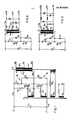
- the frequency converter for a switched mode power supply comprises a first transformer Tl whose secondary comprises a series of windings Al, A2 which supply various voltages at a series of output terminals Ul, U2, reference to a terminal Uo, for example for supplying an assembly of electronic circuits.
- the transformer Tl further comprises a primary winding Ao which is supplied by means of two conductors Mo and Ml energised at high voltage, which voltage is produced by a rectifier circuit in a known manner which will not be described herein.
- the conductor Mo is connected to one end of the winding Ao.
- the opposite end of the primary winding Ao is connected to two control circuits Pl and P2, each of which comprises a transistor Q1 and Q2 and a diode Dl and D2 connected to the respective transistor in anti-parallel, i.e. the forward directions of the diode and the transistor are opposite.
- the two transistors Ql and Q2 are connected in series with each other and the two diodes Dl and D2 are connected in series with each other, while the said opposite end of the primary winding Ao is connected by means of a conductor M2 to the junction between the two transistors Ql and Q2 and the two diodes Dl and D2.
- the two transistors Ql and Q2 are controlled at their bases by respective secondary windings Wl and W2 of a second transformer T2.
- the two windings Wl and W2 are oppositely poled and are connected at one end to their' transistors by way impedances Zl and Z2 respectively.
- the opposite end of the winding Wl is connected to the second supply conductor M1 from the rectifier circuit while the opposite end of the winding W2 is connected to the conductor M2.
- the primary of tne transformer T2 comprises a winding W3 which is connected by way of a resistor R3 to a winding A3 of the transformer Tl, whereby a signal corresponding to the votlage waves produced by the transformer Tl at the outputs Ul and U2 is fed back to the primary of the transformer T2.
- each control circuit Pl and P2 Associated with each control circuit Pl and P2 is a respective capacitor Cl and C2 which is capable of accumulating energy in one phase of operation and restoring it in a subsequent phase.
- the capacitor Cl is connected between the conductor Mo and the conductor M1 and thus the emitter of the transistor Ql, while the capacitor C2 is connected between the conductor Mo and the collector of the transistor Q2.
- a resistor Ro between the conductor Mo and the base of the transistor Q 1 serves for starting the converter.
- the rectifier circuit When the rectifier circuit is energised, at the beginning the supply current therefrom passes through the resistor Ro and excites the transistor Ql. Consequently, the current flowing through the transistor Ql also passes through the primary Ao of the transformer Tl thereby constituting the magnetising current of the transformer Tl. The latter, by way of the winding A3, excites the winding W3, thereby also magnetising the transformer T2.
- the winding W1 now provides control for the base of the transistor Ql which remains conductive whereby the current Im in the winding Ao goes from the collector to the emitter of the transistor Ql (see Figure 5) and partially discharges the capacitor Cl.
- the winding W2 meanwhile holds the transistor Q2 in an off condition.
- the winding W2 now provides for control of the base of the transistor Q2 which is switched on.
- the capacitor C2 begins to discharge to the transformer Tl by way of the transistor Q2 which is already switched on, thus reversing the direction of the current Im, as indicated in Figure 7. That condition continues until the transformer T2 then reaches a condition of saturation, the transistor Q2 losing its turn-on control.
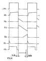
- the diagram -VF1 shows the voltage of the fed back to transformer Tl which provides for control of the transistors Qi and Q2.
- the diagram IQl indicates the current flowing through the transistor Ql, which discharges the capacitor Cl in the phase shown in Figure 5.
- the diagram ID2 shows the current which flows through the diode D2, going on to charge the capacitor C2 in the phase shown in Figure 6.
- the diagram IC2 indicates the complete waveform of the current in the capacitor C2 also in the phase shown in Figure 7 while the diagram IQ2 indicates the current flowing through the Q2 in the same phase.
- the diagram IDl shows the rapid reversal in the direction of current in the winding,Ao by way of the diode Dl in the phase shown in Figure 8.
- the diagram VF2 shows the voltage in the transformer T2, which effects control of the transistors Ql and Q2.
- the falling edge of the negative half-wave of the voltage VF2 is delayed with respect to the falling edge of the positive half-wave because of the storage time Ts of the transistor Ql, while the rising edge of the positive half-wave is delayed with respect to the rising edge of the negative half-wave because of the storage time Ts of the transistor Q2.
- the time required by the transformer T2 to attain its two states of saturation is independent of the load on the outputs, whereby the frequency of the self-oscillation is also independent.
- the ratio between the times for which the transistors Ql and Q2 are conducting primarily depends on the time taken by the transformer T2 to reach the two states of saturation; that of the positive quadrant of the hysteresis cycle in the phases shown in Figures 5 nd 8, and that of the negative quadrant of the hysteresis cycle in the phases shown in Figures 6 and 7. That ratio may be varied by returning to a winding Wc a direct current component derived from an error voltage Ve which is produced by comparing a reference voltage with one of the given output voltages, for example a voltage of 5V.
- the transformer T2 is thus biased and puts forward the time of saturation in one direction and delays it in the opposite direction.
- Such variation in the ratio of the conducting times of the two transistors Ql and Q2 of the converter permits stabilisation of the voltages at the output since it is proportional to the ratio of the on-off times ot the transistors Q1 and Q2.
- reaction signal Ve for controlling the output voltage is applied directly to T2 which causes control of the transistors Ql and Q2 and causes them to self- oscillate, thus also readily achieving the isolation necessary between the primary and secondary circuits of Tl.
- Tne secondary windings Al and A2 of the transformer T1 may be in phase opposition to the winding Ao and, by means of a pair of diodes D3 and D4 (see Figure 2) which conduct in opposition to the transistor Ql, a converter of flyback type is provided.
- the secondary windings Al and A2 disposed in phase with the primary winding Ao (see Figure 3), the arrangement provides for forward type conduction in phase with that of the transistor Ql.
- the different arrangement of the outputs does not however affect the control circuits P1 and P2.
Landscapes
- Engineering & Computer Science (AREA)
- Power Engineering (AREA)
- Dc-Dc Converters (AREA)
Applications Claiming Priority (2)
| Application Number | Priority Date | Filing Date | Title |
|---|---|---|---|
| IT6774983 | 1983-07-11 | ||
| IT67749/83A IT1161493B (it) | 1983-07-11 | 1983-07-11 | Convertitore di corrente continua per alimentatori stabilizzati tipo switching |
Publications (2)
| Publication Number | Publication Date |
|---|---|
| EP0132058A1 true EP0132058A1 (fr) | 1985-01-23 |
| EP0132058B1 EP0132058B1 (fr) | 1988-10-05 |
Family
ID=11304991
Family Applications (1)
| Application Number | Title | Priority Date | Filing Date |
|---|---|---|---|
| EP84304184A Expired EP0132058B1 (fr) | 1983-07-11 | 1984-06-21 | Convertisseur de courant continu à commutation |
Country Status (4)
| Country | Link |
|---|---|
| US (1) | US4609981A (fr) |
| EP (1) | EP0132058B1 (fr) |
| DE (1) | DE3474488D1 (fr) |
| IT (1) | IT1161493B (fr) |
Cited By (1)
| Publication number | Priority date | Publication date | Assignee | Title |
|---|---|---|---|---|
| EP0222441A1 (fr) * | 1985-11-04 | 1987-05-20 | Koninklijke Philips Electronics N.V. | Onduleur pour démarrer et alimenter une lampe à décharge |
Families Citing this family (2)
| Publication number | Priority date | Publication date | Assignee | Title |
|---|---|---|---|---|
| US8887790B2 (en) * | 2011-09-13 | 2014-11-18 | Rytec Corporation | Wind lock configuration for overhead roll-up doors |
| EP4582665A3 (fr) | 2018-11-30 | 2025-12-17 | Rytec Corporation | Ensemble porte ayant un panneau de porte à fond souple |
Citations (2)
| Publication number | Priority date | Publication date | Assignee | Title |
|---|---|---|---|---|
| US3596165A (en) * | 1969-07-24 | 1971-07-27 | Tektronix Inc | Converter circuit having a controlled output |
| FR2475819A1 (fr) * | 1980-02-08 | 1981-08-14 | Kopperschmidt Spritztech | Disposition de circuit pour produire une haute tension electrostatique obtenue a partir de la tension alternative d'un reseau de distribution, pour pistolets de pulverisation a main |
Family Cites Families (5)
| Publication number | Priority date | Publication date | Assignee | Title |
|---|---|---|---|---|
| US3539905A (en) * | 1968-11-14 | 1970-11-10 | Nasa | Saturation current protection apparatus for saturable core transformers |
| US4158881A (en) * | 1978-06-12 | 1979-06-19 | Litton Systems, Inc. | DC to DC converter |
| SU892614A1 (ru) * | 1980-04-11 | 1981-12-23 | Московский Ордена Ленина Энергетический Институт | Однотактный регул тор посто нного напр жени |
| US4334267A (en) * | 1980-10-20 | 1982-06-08 | Rca Corporation | Free-running push-pull inverter |
| US4424556A (en) * | 1981-08-13 | 1984-01-03 | Matsushita Electric Industrial Co., Ltd. | Self-oscillating DC to DC converter |
-
1983
- 1983-07-11 IT IT67749/83A patent/IT1161493B/it active
-
1984
- 1984-06-21 EP EP84304184A patent/EP0132058B1/fr not_active Expired
- 1984-06-21 DE DE8484304184T patent/DE3474488D1/de not_active Expired
- 1984-07-11 US US06/629,628 patent/US4609981A/en not_active Expired - Fee Related
Patent Citations (2)
| Publication number | Priority date | Publication date | Assignee | Title |
|---|---|---|---|---|
| US3596165A (en) * | 1969-07-24 | 1971-07-27 | Tektronix Inc | Converter circuit having a controlled output |
| FR2475819A1 (fr) * | 1980-02-08 | 1981-08-14 | Kopperschmidt Spritztech | Disposition de circuit pour produire une haute tension electrostatique obtenue a partir de la tension alternative d'un reseau de distribution, pour pistolets de pulverisation a main |
Cited By (1)
| Publication number | Priority date | Publication date | Assignee | Title |
|---|---|---|---|---|
| EP0222441A1 (fr) * | 1985-11-04 | 1987-05-20 | Koninklijke Philips Electronics N.V. | Onduleur pour démarrer et alimenter une lampe à décharge |
Also Published As
| Publication number | Publication date |
|---|---|
| US4609981A (en) | 1986-09-02 |
| DE3474488D1 (en) | 1988-11-10 |
| IT8367749A0 (it) | 1983-07-11 |
| IT1161493B (it) | 1987-03-18 |
| EP0132058B1 (fr) | 1988-10-05 |
Similar Documents
| Publication | Publication Date | Title |
|---|---|---|
| US4344122A (en) | Current sourced inverter with saturating output transformer | |
| EP0055064B2 (fr) | Convertisseur de courant continu en courant continu | |
| US3582758A (en) | Rectifier using low saturation voltage transistors | |
| US4758937A (en) | DC-DC converter | |
| EP0188839B1 (fr) | Dispositif d'alimentation en auto-oscillation | |
| EP0647011B1 (fr) | Circuit d'alimentation à haute tension | |
| US4763236A (en) | DC-DC converter | |
| US4763235A (en) | DC-DC converter | |
| US4833582A (en) | Frequency converter circuit including a single-ended blocking frequency converter | |
| US5282122A (en) | High voltage power supply topology suited for miniaturization | |
| US3843919A (en) | Dc-to-dc converter | |
| US3697851A (en) | Regulating converter circuit | |
| US4138715A (en) | Resonant switching converter | |
| US5189601A (en) | Half bridge converter with current mode controller | |
| US6744647B2 (en) | Parallel connected converters apparatus and methods using switching cycle with energy holding state | |
| US3663941A (en) | Dc to ac to dc converter having transistor synchronous rectifiers | |
| EP0484610A1 (fr) | Alimentation à découpage en courant continu avec tension de sortie contrôlée et isolation entre sortie et entrée | |
| US4672517A (en) | Switched power supply of the forward converter type | |
| US4276587A (en) | DC to DC Converter | |
| US3898549A (en) | Variable duty cycle balanced DC/DC power converter | |
| PL118673B1 (en) | Controlled deflection system | |
| EP0132058A1 (fr) | Convertisseur de courant continu à commutation | |
| US3789289A (en) | Voltage level control for d. c.-to-d. c. converter | |
| US3806792A (en) | Parallel inverter with saturable reactor current control | |
| US3959711A (en) | Pulse width modulated power supplies |
Legal Events
| Date | Code | Title | Description |
|---|---|---|---|
| PUAI | Public reference made under article 153(3) epc to a published international application that has entered the european phase |
Free format text: ORIGINAL CODE: 0009012 |
|
| AK | Designated contracting states |
Designated state(s): DE FR GB |
|
| 17P | Request for examination filed |
Effective date: 19850705 |
|
| 17Q | First examination report despatched |
Effective date: 19860515 |
|
| GRAA | (expected) grant |
Free format text: ORIGINAL CODE: 0009210 |
|
| AK | Designated contracting states |
Kind code of ref document: B1 Designated state(s): DE FR GB |
|
| REF | Corresponds to: |
Ref document number: 3474488 Country of ref document: DE Date of ref document: 19881110 |
|
| ET | Fr: translation filed | ||
| PLBE | No opposition filed within time limit |
Free format text: ORIGINAL CODE: 0009261 |
|
| STAA | Information on the status of an ep patent application or granted ep patent |
Free format text: STATUS: NO OPPOSITION FILED WITHIN TIME LIMIT |
|
| 26N | No opposition filed | ||
| PGFP | Annual fee paid to national office [announced via postgrant information from national office to epo] |
Ref country code: GB Payment date: 19920505 Year of fee payment: 9 |
|
| PGFP | Annual fee paid to national office [announced via postgrant information from national office to epo] |
Ref country code: FR Payment date: 19920609 Year of fee payment: 9 |
|
| PGFP | Annual fee paid to national office [announced via postgrant information from national office to epo] |
Ref country code: DE Payment date: 19920709 Year of fee payment: 9 |
|
| PG25 | Lapsed in a contracting state [announced via postgrant information from national office to epo] |
Ref country code: GB Effective date: 19930621 |
|
| GBPC | Gb: european patent ceased through non-payment of renewal fee |
Effective date: 19930621 |
|
| PG25 | Lapsed in a contracting state [announced via postgrant information from national office to epo] |
Ref country code: FR Effective date: 19940228 |
|
| PG25 | Lapsed in a contracting state [announced via postgrant information from national office to epo] |
Ref country code: DE Effective date: 19940301 |
|
| REG | Reference to a national code |
Ref country code: FR Ref legal event code: ST |