EP0132139A2 - Lichtverstärker basierend auf dem magnetoelektrischen Photoeffekt - Google Patents
Lichtverstärker basierend auf dem magnetoelektrischen Photoeffekt Download PDFInfo
- Publication number
- EP0132139A2 EP0132139A2 EP84304809A EP84304809A EP0132139A2 EP 0132139 A2 EP0132139 A2 EP 0132139A2 EP 84304809 A EP84304809 A EP 84304809A EP 84304809 A EP84304809 A EP 84304809A EP 0132139 A2 EP0132139 A2 EP 0132139A2
- Authority
- EP
- European Patent Office
- Prior art keywords
- light
- magnetic field
- amplifier
- intensity
- semiconductor
- Prior art date
- Legal status (The legal status is an assumption and is not a legal conclusion. Google has not performed a legal analysis and makes no representation as to the accuracy of the status listed.)
- Granted
Links
Images


Classifications
-
- H—ELECTRICITY
- H01—ELECTRIC ELEMENTS
- H01S—DEVICES USING THE PROCESS OF LIGHT AMPLIFICATION BY STIMULATED EMISSION OF RADIATION [LASER] TO AMPLIFY OR GENERATE LIGHT; DEVICES USING STIMULATED EMISSION OF ELECTROMAGNETIC RADIATION IN WAVE RANGES OTHER THAN OPTICAL
- H01S5/00—Semiconductor lasers
- H01S5/06—Arrangements for controlling the laser output parameters, e.g. by operating on the active medium
- H01S5/0607—Arrangements for controlling the laser output parameters, e.g. by operating on the active medium by varying physical parameters other than the potential of the electrodes, e.g. by an electric or magnetic field, mechanical deformation, pressure, light, temperature
-
- H—ELECTRICITY
- H01—ELECTRIC ELEMENTS
- H01S—DEVICES USING THE PROCESS OF LIGHT AMPLIFICATION BY STIMULATED EMISSION OF RADIATION [LASER] TO AMPLIFY OR GENERATE LIGHT; DEVICES USING STIMULATED EMISSION OF ELECTROMAGNETIC RADIATION IN WAVE RANGES OTHER THAN OPTICAL
- H01S5/00—Semiconductor lasers
- H01S5/50—Amplifier structures not provided for in groups H01S5/02 - H01S5/30
-
- H—ELECTRICITY
- H01—ELECTRIC ELEMENTS
- H01S—DEVICES USING THE PROCESS OF LIGHT AMPLIFICATION BY STIMULATED EMISSION OF RADIATION [LASER] TO AMPLIFY OR GENERATE LIGHT; DEVICES USING STIMULATED EMISSION OF ELECTROMAGNETIC RADIATION IN WAVE RANGES OTHER THAN OPTICAL
- H01S5/00—Semiconductor lasers
- H01S5/20—Structure or shape of the semiconductor body to guide the optical wave ; Confining structures perpendicular to the optical axis, e.g. index or gain guiding, stripe geometry, broad area lasers, gain tailoring, transverse or lateral reflectors, special cladding structures, MQW barrier reflection layers
- H01S5/22—Structure or shape of the semiconductor body to guide the optical wave ; Confining structures perpendicular to the optical axis, e.g. index or gain guiding, stripe geometry, broad area lasers, gain tailoring, transverse or lateral reflectors, special cladding structures, MQW barrier reflection layers having a ridge or stripe structure
- H01S5/223—Buried stripe structure
-
- H—ELECTRICITY
- H01—ELECTRIC ELEMENTS
- H01S—DEVICES USING THE PROCESS OF LIGHT AMPLIFICATION BY STIMULATED EMISSION OF RADIATION [LASER] TO AMPLIFY OR GENERATE LIGHT; DEVICES USING STIMULATED EMISSION OF ELECTROMAGNETIC RADIATION IN WAVE RANGES OTHER THAN OPTICAL
- H01S5/00—Semiconductor lasers
- H01S5/30—Structure or shape of the active region; Materials used for the active region
- H01S5/32—Structure or shape of the active region; Materials used for the active region comprising PN junctions, e.g. hetero- or double- heterostructures
- H01S5/3222—Structure or shape of the active region; Materials used for the active region comprising PN junctions, e.g. hetero- or double- heterostructures in AIVBVI compounds, e.g. PbSSe-laser
-
- H—ELECTRICITY
- H01—ELECTRIC ELEMENTS
- H01S—DEVICES USING THE PROCESS OF LIGHT AMPLIFICATION BY STIMULATED EMISSION OF RADIATION [LASER] TO AMPLIFY OR GENERATE LIGHT; DEVICES USING STIMULATED EMISSION OF ELECTROMAGNETIC RADIATION IN WAVE RANGES OTHER THAN OPTICAL
- H01S5/00—Semiconductor lasers
- H01S5/30—Structure or shape of the active region; Materials used for the active region
- H01S5/32—Structure or shape of the active region; Materials used for the active region comprising PN junctions, e.g. hetero- or double- heterostructures
- H01S5/327—Structure or shape of the active region; Materials used for the active region comprising PN junctions, e.g. hetero- or double- heterostructures in AIIBVI compounds, e.g. ZnCdSe-laser
Definitions
- the present invention relates to a light amplifier formed of a semiconductor material provided with the faculty of light amplification based on the magnetoelectric-photo effect, particularly, at the room temperature, as well as over a wide range of wavelength at low temperatures such as liquid helium temperature.
- a light amplifier according to the principle that the light amplification is effected by the stimulated emission from the activated amplifying medium, such as a light amplifier consisting of a semiconductor material in which a population inversion region of electrons and holes is formed on the basis of light pumping effected by a gas laser, a solid-state laser and the like, and a light amplifier consisting of a p-n junction semiconductor material having a population inversion region of electrons and holes in the central portion of the junction region applied with the forward current, has been employed.
- a light amplifier consisting of a semiconductor material in which a population inversion region of electrons and holes is formed on the basis of light pumping effected by a gas laser, a solid-state laser and the like
- a light amplifier consisting of a p-n junction semiconductor material having a population inversion region of electrons and holes in the central portion of the junction region applied with the forward current
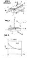
- the width of active region is restricted so narrow as the diffusion length of the carrier, for instance, in the order of 10 ⁇ m. That is, in a p-n junction type laser diode as shown in Fig. 1, a p-n junction region 3 arranged between an n-type semiconductor substrate 1 and a p-type semiconductor layer 2 is applied with a bias voltage through lead wires 6 and 7, and, in this situation, an input light through an end surface 4 polished into a mirror surface is intensified and taken out of an opposite surface 5 as a laser beam 8.
- the width of the p-n junction 3 appearing on the input surface 4 is extremely narrow as mentioned above, so that it is very difficult to get the input light coupled with the extremely narrow end surface of the p-n junction region 3.
- the conventional semiconductor light amplifier has the serious defect of inconvenience in practical use.
- the object of the present invention is to remove the above mentioned defect from the conventional semiconductor light amplifier and to provide a semiconductor light amplifier based on a new principle of the light amplification through the magnetoelectric-photo effect, which can be operated at room temperature for wavelengths longer than -2 ⁇ m and makes it possible to change the wavelength of the output light as well as having wide area of the surface for the incident light.
- the accomplishment of the object would bring remarkable merits in practical use, such that the inconvenience in practical use, due to the use of bulky dewar as well as the use of refrigerant such as liquid nitrogen for refrigirating the device, can be dissolved and hence the device can be miniaturized, in addition, the coupling of the input light with the active region thereof can easily be achieved over the wide range of wavelength.
- the light amplifier using the magnetoelectric-photo effect according to the present invention is based on a new principle quite different from the conventional principle of light amplification that a population inversion region is formed by supplying a large forward current through a p-n junction type semiconductor material, and, as a result thereof, a solid-state light amplifier which can be operated over the wide range of temperature from the liquid helium temperature of 4.2°K to room temperature as well as over the wide range of wavelength from far infrared to vacuum-ultraviolet, can be realized.
- the light amplifier according to present invention is featured in that a semiconductor block consisting of material, having the mobility of electrons and holes corresponding at least to the magnetic-field intensity, is disposed in the magnetic field having the field intensity concerned, that is generated by a permanent magnet or an electromagnet, and a polulation inversion region of electrons and holes is formed along a surface crossing mutually opposed surfaces of the semiconductor block therein by the Lorentz force generated by supplying an electric current through electrodes provided on the mutually opposed surfaces respectively, and, as a result thereof, the light which is incident from an opposite surface to the crossing surface and passes through the population inversion region of electrons and holes is amplified and emitted from the crossing surface.
- the conventional inconveniences in practical use have not been dissolved, but, for instance, on the operation at liquid helium temperature, it is also capable of getting an intensified output light having arbitrary wavelength over its wide range corresponding to the intensity of the applied magnetic field. So that various excellent functions and effects, such that the light amplifier according to the present invention can be applicable to the light intensifier, the semiconductor laser of tunable wavelength and the like, can be obtained.
- a semiconductor flat plate 9 of a thickness d having no electrons and p o holes per unit volume in thermal equilibrium state is supplied with a current II in the longitudinal direction parallel with X-axis thereof, as well as applied with a magnetic field of intensity]H in the transversal direction parallel with Z-axis thereof.
- the magnetic field intensity IH is so high as the condition of intense magnetic field is satisfied
- electrons ⁇ and holes ⁇ are swept together, as shown by dashed lines in Fig. 2, in -y direction by the Lorentz force based on the co-operation of the magnetic field IH and the current II.
- the excess electron-hole pairs are to be annihilated by the recombination therebetween in the vicinity of the light-emitting surface.
- a light 11 having a central wavelength ⁇ 0 substantially corresponding to the energy gap Eg of the semiconductor material employed, and hence expressed by the following expression (2), is emitted; where c is the light velocity, h is Planck's constant, k is Boltzmann constant, and T is the absolute temperature.
- the emitted intensity of the above mentioned light having the central wavelength ⁇ o depends nonlinearly on the supplied current density J and the applied magnetic field intensity H; the emitted intensity is proportional to the rate R c of the radiative recombination per unit volume and per unit time in non- equilibrium state, which is expressed by the following expression (3); with where, R and B are the rate and the probability of radiative recombination in thermal equilibrium respectively, n i is the intrinsic carrier concentration as mentioned earlier, and y is a parameter approximated by the following expression (5) related to the thickness d of the semiconductor flat plate. where no is the electron concentration of the semiconductor material.
- the population of electrons and holes when the above mentioned population inversion is caused by the JxH force, that is, the Lorentz force acting along the -y direction is schematically shown in one dimension like along the y direction in Fig. 4. It has been clarified from the experiment carried out by the inventor that the depletion region formed in the vicinity of the rear surface opposite to the light-emitting surface 10 of the semiconductor flat plate 9 as shown in Fig. 2 is compensated by electrons and holes generated by the absorption of the background radiation, so that the population inversion region occupies much wider portion of the semiconductor flat plate than the depletion region.
- the light amplification with variable wavelength can be effected by adjusting the intensity of magnetic field applied thereon, as well as an intense monochromatic light source can be realized.
- h is a constant having the relation with Planck's constant h
- e is the electric charge of the electron
- c is the light velocity
- H is the magnetic field intensity.
- a monochromatic light source having further shorter wavelength for instance, a vacuum-ultraviolet light source by employing an electron-beam excitation in place of the photo-excitation.
- a semiconductor laser operating in extremely wide range of wavelengths by empolying suitable feedback using an additional resonator.
- the light amplifier according to the present invention has not only a valuable kind of practical application thereof.
- the wavelength of the emission changes corresponding to the energy gap Eg of the used semiconductor materials, as expressed by expression (2) or by expression (7) for the operation at liquid helium temperature. Consequently, it is also possible to amplify the light over the wide range of wavelength from far-infrared to vacuum-ultraviolet.
- the light amplifier according to the present invention all kinds of semiconductor materials can be employed in principle. However, it is preferable, in relation with the intensity of magnetic field required for composing the light amplifier of the present invention, to employ the semiconductor material having high mobilities of electrons and holes, that is, small effective masses m of electrons and holes.
- FIG. 5 A fundamental configuration of the light amplifier of the present invention for effecting the light amplification based on the above detailed operational principle is shown in Fig. 5.
- a flat plate 13 of semiconductor material as exemplified in Table 1 is disposed between poles N and S of a permanent or electromagnet 12 forming an intense magnetic field over ten thousands gausses.
- An electric current I in a form of dc, ac or pulse is supplied from an external power source 14 through electrodes deposited respectively on both end surfaces of the semiconductor flat plate 13.
- the electrodes deposited on both end surfaces of the semiconductor flat plates 13 can be formed of so-called ohmic electrodes simply used for supplying the electric current, as well as of semiconductor electrodes acting for both of current supply and injection of minority carriers into the semiconductor material.
- the light amplifier according to the present invention has not'only the feature that it can be operated in the intrinsic region of semiconductor materials under the satisfication of the aforesaid condition of intense magnetic field, but also generally includes all of the devices which effect the light amplification based on the population inversion of electrons and holes, formed by the so-called Lorentz force, that is, the JxH force originated from the interaction of the supplied electric current I with the applied magnetic field H, naturally including the aforesaid situation where the condition of the applied magnetic field intensity is mitigated by injecting minority carriers into the semiconductor flat plate through electrodes attached thereto as mentioned earlier.
- an InSb flat plate 15 with an effective size being 11 mm long, 4.0 mm wide and 0.88 mm thick was employed.
- This sample has the values of the electron concentration n and the 0 Hall mobility p being 5 ⁇ 10 15 cm- 3 and 1 .
- This sample 15 was mounted in a metal dewar having a Ge window 17 of 9 mm effective diameter which works as a 5.3 ⁇ m bandpass filter, and was supplied with a pulsed current having a pulse width of 20 ⁇ s, a repetition rate of 50 Hz and an intensity up to 6 A by a pulse generator 24, as well as with an ac current having an intensity up to 200 mA at a frequency of 250 Hz or a dc current optionally, and further was subjected to a dc magnetic field H having an intensity up to 20 K gausses by an electromagnet across the supplied current.
- an output light of an Ar + laser 18 cw operated at a wavelength of 514.5 nm with a power from 100 to 900 mW was converted into a rectangular pulsed light of a frequency 50 Hz through a chopper 19 and then the rear surface of the sample 15 was irradiated by the light through a sapphire window 16 and an aperture of 3 mm diameter, so as to generate the required input light of wavelength -5.3 ⁇ m from the photo-luminescence associated with the above photo-excitation, as shown in Fig. 7.
- the amplified output light from the sample 15 was taken out of a Ge window 17 having a maximum transmittance at 5.3 ⁇ m and then fed into to an InSb infrared radiation detector 21 mounted in another metal dewar through a light pipe 20 of 50 cm length.
- the photosignal from the detector 21 which was modulated at 50 Hz or 250 Hz was synchronously detected by a lock-in amplifier 22.
- the waveform of the detected output signal derived from the amplifier 22 was indicated on a cathode-ray display 23.
- the intensity of the radiation emitted from the InSb sample is much increased, when the irradiation power of the exiting laser exceeds 500 mW.
- an InSb flat plate in Fig. 8 was irradiated by the chopped Ar + laser beam of 800 mW at a frequency of 50 Hz, so as to generate the input light having a wavelength of 5.3 ⁇ m from the photo-luminescence by the photo-excitation.
- dc pulsed current up to 6 A with 20 ps width was synchronously passed through the sample across the applied magnetic field of 20 K gausses, and the output light from the semiconductor flat plate 15 was synchronously detected by the combination of the narrow band InSb infrared detector 21 and the lock-in amplifier 22 through the 5.3 pm bandpass Ge filter 17.
- Figs. 9 and 10 Thus detected intensity of the output radiation, which is normalized by the intensity of the photo-luminescence in the absence of any applied magnetic field and electric current, is shown in Figs. 9 and 10.
- the data as shown in Fig. 10 indicate the similar results measured at room temperature of 292°K. Both these data are corrected, so as to have the same duty ratio, taking into account the difference in the pulse densities, namely, duty ratios between the pulsed current supplied and the chopped laser irradiation.
- the negative amplification namely, the absorption of the background light is effected in the vicinity of the light-emitting surface of the semiconductor sample in the range of the supplied current intensity, I ⁇ 4 A.
- This absorption of the background light results from the fact that, in the situation where H ⁇ 0, namely, the magnetic field of negative polarity is applied, the excess electron-hole pairs concentrate in the vicinity of the rear surface of the semiconductor flat plate, while the depletion region is formed in the vicinity of the light-emitting surface thereof, and hence the absorption of the background radiation occurs in this depletion region, so as to compensate the decrease of -the carrier, concentration therein.
- the light amplifier based on the above new operational principle according to the present invention which is formed of various kinds of semiconductor materials having respectively different energy gaps, for instance, as shown in Table 1, it is posssible to intensity the incident light having wavelength in wide range from far infrared to vacuum-ultraviolet, furthermore it is also possible to easily modulate the intensified output light through controlling the current intensity supplied thereto.
- the light amplification can be readily attained in the extremely wide range of wavelengths and at the wide range of temperatures from liquid helium temperature to about 100°C over room temperature, so far as the condition of intense magnetic field is satisfied.
- the efficiency of this light amplification can be raised by spreading the population inversion region of electrons and holes in the direction of thickness of the semiconductor flat plate through the suitable surface treatments on the semiconductor material. It is also effective for a certain kind of semiconductor materials to inject the minority carriers thereinto through suitable injection electrodes provided thereon, so as to increase the effect of the application of magnetic field.
- the carrier based on the photo-excitation are generated by irradiating the rear surface of the semiconductor flat plate with incident light having a shorter wavelength than that corresponding to the energy gap of the semiconductor material concerned, and the. concentration of excess electron-hole pairs in the vicinity of the light-emitting surface thereof can be increased by the action of the JxH force and hence it is possible to control the wavelength of the intensified output light corresponding to the intensity of the applied magnetic field, so as to utilize the light amplifier concerned as a monochromatic light source having a tunable wavelength; furthermore it is possible to utilize it as a laser having a tunable wavelength by attaching an appropriate resonator thereto.
- the infrared radiation having a wavelength ranging from 8 to 14 pm can be utilized for the wireless communication in the space or between the ground stations.
- a transmitting and a receiving light amplifiers are indispensable for these wireless communications. Moreover, special performances such-as these light amplifiers are to be operated at room temperature with the large amplification factor and provided with large light-receiving surfaces facilitating the coupling with the incident light is required.
- the light amplifier according to the present invention which can be operated in the above mentioned range of wavelength, for example, a semiconductor material consisting of mercury cadmium telluride Hg l -x Cd x Te having the composition ratio x ⁇ 0.2 is provided with the faculty of amplifying the light having a wavelength close to 12.4 pm. This light amplifier can be used for a laser diode by applying suitable feedback thereto, so as to utilize it as a transmitting light source.
- FIG. 11(a) The outline of the configuration of this infrared wireless communication apparatus is shown in Fig. 11(a).
- the magnetoelectric-photo effect according to the present invention is applied to an infrared emitting diode laser 27, so as to emit the infrared radiation at a wavelength of 12.4 pm, and as for the current to be supplied to the diode concerned, the current at audio frequency derived from the microphone 25 and amplified through the low frequency amplifier 26 is employed.
- the infrared photosignal which is intensity- modulated by the current at audio frequency can be obtained.
- This infrared photosignal amplified through the light amplifier 28 according to the present invention is sent into the photo transmission medium 30 through the transmitting optical system 29.
- the intensity of the photosignal attenuates, and so it is necessary to repeatedly amplify the attenuated photosignal through the repeater amplifiers arranged at every adequate transmission distances.
- the repeater amplifier an indirect-type light amplifier, in which the electric signal once converted from the photosignal and power-amplified is reconverted to the photosignal through light-emitting diodes, as conventionally conceived; however the quality of the photosignal such as the amount of information contained therein and the signal to noise ratio is much deteriorated through the conversion process.
- the light amplifier according to the present invention can be operated at room temperature and has the large amplification factor and the large light-receiving surface facilitating the direct coupling with the incident light, and hence the ideal operation required for the repeater amplifier used for the photo communication can be expected therethrough.
- the photosignal propagating through the photo transmission medium 36 is repeatedly amplified by the light amplifiers 38 and 39 through the receiving optical system 37, as well as the distortion of waveform of the photosignal, which is caused during the transmission, is corrected through the signal waveform restorer 40, and thereafter the amplified and corrected photosignal is transmitted again through the photo transmission medium 42.
- the photo transmission medium in the wireless communication system as shown in Figs. ll(a), (b) is to be replaced with the optical fiber, as well as a gallium arsenide compound GaAs which can operate at the wavelength close to 0.87 pm is to be selected for the semiconductor material forming the light amplifier according to the present invention.
- the arrangements as shown in Figs. 11(a), (b) can be utilized as the communication apparatus.
- a light amplifier which can operate at room temperature, by applying an intense magnetic field, for instance, by a permanent magnet, to a semiconductor material through which a current is passed.
- an intense monochromatic light source namely, a laser having a tunable wavelength corresponding to the intensity of the magnetic field applied thereon by a superconductive electromagnet, in the situation where the light amplifier concerned is operated at low temperature such as liquid helium temperature with photo-excitation.
- the conventional p-n junction type semiconductor laser has a defect such that the area for receiving the incident light is extremely narrow, and hence it is difficult to couple the incident light therewith, in addition it has also the defect that it only can be operated at low temperatures at lower temperature than liquid nitrogen temperature for the generation of medium infrared radiation longer than -2 ⁇ m wavelength.
- the light amplifier based on the magnetoelectric-photo effect according to the present invention has numerous remarkable advantages such that it can be operated fundamentally at room temperature, and that the area for receiving the incident light is not only much broader than the conventional one, but it is also possible to obtain a light amplification factor exceeding 200 times per stage. Accordingly, it can be expected that the light amplifier according to the present invention is utilized for the repeater amplifier in the optical communication system employing the optical fiber, or, the light amplifier for the wireless communication using the infrared radiation of wavelength from 8 to 14 pm.
- the light amplifier according to the present invention is more effectively utilized as the intense light source generating tunable wavelength of radiation suitable for the wireless communication system than with the conventional spin-flip Raman laser which has been available today.
- the conventional spin-flip Raman laser generates actually the tunable wavelength of radiation corresponding to the intensity of the magnetic field applied at liquid helium temperatures; however, it is operated by using the spin flip Raman effect, and so the power efficiency factor thereof is distinctly smaller than that of the light amplifier according to the present invention.
Landscapes
- Physics & Mathematics (AREA)
- Condensed Matter Physics & Semiconductors (AREA)
- General Physics & Mathematics (AREA)
- Electromagnetism (AREA)
- Optics & Photonics (AREA)
- Semiconductor Lasers (AREA)
- Lasers (AREA)
- Light Receiving Elements (AREA)
Applications Claiming Priority (2)
| Application Number | Priority Date | Filing Date | Title |
|---|---|---|---|
| JP128708/83 | 1983-07-16 | ||
| JP58128708A JPS6021588A (ja) | 1983-07-16 | 1983-07-16 | 磁気電気光効果光増幅器 |
Publications (3)
| Publication Number | Publication Date |
|---|---|
| EP0132139A2 true EP0132139A2 (de) | 1985-01-23 |
| EP0132139A3 EP0132139A3 (en) | 1985-04-10 |
| EP0132139B1 EP0132139B1 (de) | 1989-05-31 |
Family
ID=14991461
Family Applications (1)
| Application Number | Title | Priority Date | Filing Date |
|---|---|---|---|
| EP84304809A Expired EP0132139B1 (de) | 1983-07-16 | 1984-07-13 | Lichtverstärker basierend auf dem magnetoelektrischen Photoeffekt |
Country Status (4)
| Country | Link |
|---|---|
| US (1) | US4749952A (de) |
| EP (1) | EP0132139B1 (de) |
| JP (1) | JPS6021588A (de) |
| DE (1) | DE3478541D1 (de) |
Cited By (2)
| Publication number | Priority date | Publication date | Assignee | Title |
|---|---|---|---|---|
| EP0255959A1 (de) * | 1986-08-08 | 1988-02-17 | Sumitomo Electric Industries Limited | Magneto-elektro-optischer Lichtmodulator |
| GB2309583A (en) * | 1996-01-29 | 1997-07-30 | Eizo Ishikawa | An electromagnetic radiation device |
Families Citing this family (9)
| Publication number | Priority date | Publication date | Assignee | Title |
|---|---|---|---|---|
| US4952811A (en) * | 1989-06-21 | 1990-08-28 | The United States Of America As Represented By The Administrator Of The National Aeronautics And Space Administration | Field induced gap infrared detector |
| US6953703B2 (en) | 1991-03-18 | 2005-10-11 | The Trustees Of Boston University | Method of making a semiconductor device with exposure of sapphire substrate to activated nitrogen |
| CA2070708C (en) * | 1991-08-08 | 1997-04-29 | Ichiro Kasai | Visible and infrared indium antimonide (insb) photodetector with non-flashing light receiving surface |
| US5784397A (en) * | 1995-11-16 | 1998-07-21 | University Of Central Florida | Bulk semiconductor lasers at submillimeter/far infrared wavelengths using a regular permanent magnet |
| US6541788B2 (en) * | 1998-10-27 | 2003-04-01 | The Regents Of The University Of California | Mid infrared and near infrared light upconverter using self-assembled quantum dots |
| US6988058B1 (en) | 1998-12-16 | 2006-01-17 | The Regents Of The University Of California | Quantum computation with quantum dots and terahertz cavity quantum electrodynamics |
| US6583436B2 (en) | 2000-06-27 | 2003-06-24 | The Regents Of The University Of California | Strain-engineered, self-assembled, semiconductor quantum dot lattices |
| SE0302191D0 (sv) * | 2003-03-10 | 2003-08-11 | Staffan Gunnarsson | Transponder med infrarödteknik |
| US20160373866A1 (en) * | 2015-06-04 | 2016-12-22 | Gordon Shaw Novak | Light Flicker to Sound Conversion |
Family Cites Families (7)
| Publication number | Priority date | Publication date | Assignee | Title |
|---|---|---|---|---|
| US3247765A (en) * | 1961-07-05 | 1966-04-26 | Ibm | Light switching means |
| JPS5120271B2 (de) * | 1972-05-01 | 1976-06-23 | ||
| JPS5348079A (en) * | 1976-10-14 | 1978-05-01 | Mitsui Eng & Shipbuild Co Ltd | Rotary kiln apparatus |
| NL7707720A (nl) * | 1977-07-12 | 1979-01-16 | Philips Nv | Halfgeleiderlaser of -versterker. |
| JPS54116187A (en) * | 1978-03-01 | 1979-09-10 | Fujitsu Ltd | Unidirectional photo amplifier |
| JPS5758376A (en) * | 1980-09-25 | 1982-04-08 | Univ Kyoto | Magnetism-infrared emitting diode |
| US4516144A (en) * | 1982-09-23 | 1985-05-07 | Eaton Corporation | Columnated and trimmed magnetically sensitive semiconductor |
-
1983
- 1983-07-16 JP JP58128708A patent/JPS6021588A/ja active Granted
-
1984
- 1984-07-13 EP EP84304809A patent/EP0132139B1/de not_active Expired
- 1984-07-13 DE DE8484304809T patent/DE3478541D1/de not_active Expired
-
1986
- 1986-10-02 US US06/914,516 patent/US4749952A/en not_active Expired - Lifetime
Cited By (3)
| Publication number | Priority date | Publication date | Assignee | Title |
|---|---|---|---|---|
| EP0255959A1 (de) * | 1986-08-08 | 1988-02-17 | Sumitomo Electric Industries Limited | Magneto-elektro-optischer Lichtmodulator |
| US4806885A (en) * | 1986-08-08 | 1989-02-21 | Sumitomo Electric Industries, Ltd. | Magnet-electro-optic effect light modulator |
| GB2309583A (en) * | 1996-01-29 | 1997-07-30 | Eizo Ishikawa | An electromagnetic radiation device |
Also Published As
| Publication number | Publication date |
|---|---|
| JPS6021588A (ja) | 1985-02-02 |
| DE3478541D1 (en) | 1989-07-06 |
| JPH0252870B2 (de) | 1990-11-14 |
| EP0132139B1 (de) | 1989-05-31 |
| US4749952A (en) | 1988-06-07 |
| EP0132139A3 (en) | 1985-04-10 |
Similar Documents
| Publication | Publication Date | Title |
|---|---|---|
| Verghese et al. | GaN avalanche photodiodes operating in linear-gain mode and Geiger mode | |
| Paoli et al. | Direct modulation of semiconductor lasers | |
| EP0132139B1 (de) | Lichtverstärker basierend auf dem magnetoelektrischen Photoeffekt | |
| Xu et al. | Terahertz radiation from large aperture Si p‐i‐n diodes | |
| US4450460A (en) | Magnetic-infrared-emitting diode | |
| Aoki et al. | Efficient backward and forward pumping CW Raman amplification for InGaAsP laser light in silica fibres | |
| EP0255959B1 (de) | Magneto-elektro-optischer Lichtmodulator | |
| Partin et al. | Wavelength coverage of lead‐europium‐selenide‐telluride diode lasers | |
| US20220190549A1 (en) | Semiconductor optical signal amplifier | |
| RU2197770C2 (ru) | Светоизлучающие диоды ик-диапазона | |
| Georgobiani | Wide-band II-VI semiconductors and the prospects of their application | |
| US4158207A (en) | Iron-doped indium phosphide semiconductor laser | |
| US3614447A (en) | Method for modulating semiconductor lasers | |
| Capasso et al. | Conversion of Poisson photons into sub-Poisson photons by the action of electron feedback | |
| Keune et al. | Spontaneous and Stimulated Carrier Lifetime and the Spectral Output of CdSe (77° K) | |
| Mermelstein et al. | Low-power photocurrent nonlinearity in quantum well infrared detectors | |
| Leotin | Far infrared photoconductive detectors | |
| Dodel et al. | Wideband heterodyne detection in the far infrared with extrinsic Ge photoconductors | |
| Rodot et al. | 9B3-Semiconductor lasers and fast detectors in the infrared (3 to 15 microns) | |
| Stone et al. | Detection of terahertz radiation by hot electron effects in coupled quantum well photodiodes | |
| De Cremoux et al. | Free-carrier absorption for 10 µ modulation | |
| Beggs et al. | Optical charge injection into a gallium arsenide acoustic charge transport device | |
| Mukai et al. | S/N performance of an AlGaAs laser preamplifier and a linear repeater system | |
| Ram et al. | Cascade semiconductor lasers for telecommunications | |
| Shirao et al. | Preliminary experiment on direct media conversion from a 1.55 µm optical signal to a sub-terahertz wave signal using photon-generated free carriers |
Legal Events
| Date | Code | Title | Description |
|---|---|---|---|
| PUAI | Public reference made under article 153(3) epc to a published international application that has entered the european phase |
Free format text: ORIGINAL CODE: 0009012 |
|
| AK | Designated contracting states |
Designated state(s): BE DE FR GB NL |
|
| PUAL | Search report despatched |
Free format text: ORIGINAL CODE: 0009013 |
|
| AK | Designated contracting states |
Designated state(s): BE DE FR GB NL |
|
| 17P | Request for examination filed |
Effective date: 19850603 |
|
| 17Q | First examination report despatched |
Effective date: 19861113 |
|
| GRAA | (expected) grant |
Free format text: ORIGINAL CODE: 0009210 |
|
| AK | Designated contracting states |
Kind code of ref document: B1 Designated state(s): BE DE FR GB NL |
|
| REF | Corresponds to: |
Ref document number: 3478541 Country of ref document: DE Date of ref document: 19890706 |
|
| ET | Fr: translation filed | ||
| PLBE | No opposition filed within time limit |
Free format text: ORIGINAL CODE: 0009261 |
|
| 26N | No opposition filed | ||
| REG | Reference to a national code |
Ref country code: GB Ref legal event code: IF02 |
|
| PGFP | Annual fee paid to national office [announced via postgrant information from national office to epo] |
Ref country code: GB Payment date: 20030709 Year of fee payment: 20 |
|
| PGFP | Annual fee paid to national office [announced via postgrant information from national office to epo] |
Ref country code: FR Payment date: 20030711 Year of fee payment: 20 |
|
| PGFP | Annual fee paid to national office [announced via postgrant information from national office to epo] |
Ref country code: DE Payment date: 20030724 Year of fee payment: 20 |
|
| PGFP | Annual fee paid to national office [announced via postgrant information from national office to epo] |
Ref country code: NL Payment date: 20030730 Year of fee payment: 20 |
|
| PGFP | Annual fee paid to national office [announced via postgrant information from national office to epo] |
Ref country code: BE Payment date: 20030922 Year of fee payment: 20 |
|
| PG25 | Lapsed in a contracting state [announced via postgrant information from national office to epo] |
Ref country code: GB Free format text: LAPSE BECAUSE OF EXPIRATION OF PROTECTION Effective date: 20040712 |
|
| PG25 | Lapsed in a contracting state [announced via postgrant information from national office to epo] |
Ref country code: NL Free format text: LAPSE BECAUSE OF EXPIRATION OF PROTECTION Effective date: 20040713 |
|
| BE20 | Be: patent expired |
Owner name: *KYOTO UNIVERSITY Effective date: 20040713 |
|
| REG | Reference to a national code |
Ref country code: GB Ref legal event code: PE20 |
|
| NLV7 | Nl: ceased due to reaching the maximum lifetime of a patent |
Effective date: 20040713 |