EP0132408A2 - Procédé et appareil pour faire croître des couches ou pour produire des revêtements sur un substrat - Google Patents
Procédé et appareil pour faire croître des couches ou pour produire des revêtements sur un substrat Download PDFInfo
- Publication number
- EP0132408A2 EP0132408A2 EP84305048A EP84305048A EP0132408A2 EP 0132408 A2 EP0132408 A2 EP 0132408A2 EP 84305048 A EP84305048 A EP 84305048A EP 84305048 A EP84305048 A EP 84305048A EP 0132408 A2 EP0132408 A2 EP 0132408A2
- Authority
- EP
- European Patent Office
- Prior art keywords
- substrate
- chamber
- growth chamber
- growth
- heating
- Prior art date
- Legal status (The legal status is an assumption and is not a legal conclusion. Google has not performed a legal analysis and makes no representation as to the accuracy of the status listed.)
- Withdrawn
Links
Images



Classifications
-
- C—CHEMISTRY; METALLURGY
- C23—COATING METALLIC MATERIAL; COATING MATERIAL WITH METALLIC MATERIAL; CHEMICAL SURFACE TREATMENT; DIFFUSION TREATMENT OF METALLIC MATERIAL; COATING BY VACUUM EVAPORATION, BY SPUTTERING, BY ION IMPLANTATION OR BY CHEMICAL VAPOUR DEPOSITION, IN GENERAL; INHIBITING CORROSION OF METALLIC MATERIAL OR INCRUSTATION IN GENERAL
- C23C—COATING METALLIC MATERIAL; COATING MATERIAL WITH METALLIC MATERIAL; SURFACE TREATMENT OF METALLIC MATERIAL BY DIFFUSION INTO THE SURFACE, BY CHEMICAL CONVERSION OR SUBSTITUTION; COATING BY VACUUM EVAPORATION, BY SPUTTERING, BY ION IMPLANTATION OR BY CHEMICAL VAPOUR DEPOSITION, IN GENERAL
- C23C16/00—Chemical coating by decomposition of gaseous compounds, without leaving reaction products of surface material in the coating, i.e. chemical vapour deposition [CVD] processes
- C23C16/44—Chemical coating by decomposition of gaseous compounds, without leaving reaction products of surface material in the coating, i.e. chemical vapour deposition [CVD] processes characterised by the method of coating
- C23C16/455—Chemical coating by decomposition of gaseous compounds, without leaving reaction products of surface material in the coating, i.e. chemical vapour deposition [CVD] processes characterised by the method of coating characterised by the method used for introducing gases into reaction chamber or for modifying gas flows in reaction chamber
- C23C16/45561—Gas plumbing upstream of the reaction chamber
-
- C—CHEMISTRY; METALLURGY
- C23—COATING METALLIC MATERIAL; COATING MATERIAL WITH METALLIC MATERIAL; CHEMICAL SURFACE TREATMENT; DIFFUSION TREATMENT OF METALLIC MATERIAL; COATING BY VACUUM EVAPORATION, BY SPUTTERING, BY ION IMPLANTATION OR BY CHEMICAL VAPOUR DEPOSITION, IN GENERAL; INHIBITING CORROSION OF METALLIC MATERIAL OR INCRUSTATION IN GENERAL
- C23C—COATING METALLIC MATERIAL; COATING MATERIAL WITH METALLIC MATERIAL; SURFACE TREATMENT OF METALLIC MATERIAL BY DIFFUSION INTO THE SURFACE, BY CHEMICAL CONVERSION OR SUBSTITUTION; COATING BY VACUUM EVAPORATION, BY SPUTTERING, BY ION IMPLANTATION OR BY CHEMICAL VAPOUR DEPOSITION, IN GENERAL
- C23C16/00—Chemical coating by decomposition of gaseous compounds, without leaving reaction products of surface material in the coating, i.e. chemical vapour deposition [CVD] processes
- C23C16/22—Chemical coating by decomposition of gaseous compounds, without leaving reaction products of surface material in the coating, i.e. chemical vapour deposition [CVD] processes characterised by the deposition of inorganic material, other than metallic material
- C23C16/30—Deposition of compounds, mixtures or solid solutions, e.g. borides, carbides, nitrides
- C23C16/301—AIII BV compounds, where A is Al, Ga, In or Tl and B is N, P, As, Sb or Bi
-
- C—CHEMISTRY; METALLURGY
- C23—COATING METALLIC MATERIAL; COATING MATERIAL WITH METALLIC MATERIAL; CHEMICAL SURFACE TREATMENT; DIFFUSION TREATMENT OF METALLIC MATERIAL; COATING BY VACUUM EVAPORATION, BY SPUTTERING, BY ION IMPLANTATION OR BY CHEMICAL VAPOUR DEPOSITION, IN GENERAL; INHIBITING CORROSION OF METALLIC MATERIAL OR INCRUSTATION IN GENERAL
- C23C—COATING METALLIC MATERIAL; COATING MATERIAL WITH METALLIC MATERIAL; SURFACE TREATMENT OF METALLIC MATERIAL BY DIFFUSION INTO THE SURFACE, BY CHEMICAL CONVERSION OR SUBSTITUTION; COATING BY VACUUM EVAPORATION, BY SPUTTERING, BY ION IMPLANTATION OR BY CHEMICAL VAPOUR DEPOSITION, IN GENERAL
- C23C16/00—Chemical coating by decomposition of gaseous compounds, without leaving reaction products of surface material in the coating, i.e. chemical vapour deposition [CVD] processes
- C23C16/22—Chemical coating by decomposition of gaseous compounds, without leaving reaction products of surface material in the coating, i.e. chemical vapour deposition [CVD] processes characterised by the deposition of inorganic material, other than metallic material
- C23C16/30—Deposition of compounds, mixtures or solid solutions, e.g. borides, carbides, nitrides
- C23C16/305—Sulfides, selenides, or tellurides
- C23C16/306—AII BVI compounds, where A is Zn, Cd or Hg and B is S, Se or Te
-
- C—CHEMISTRY; METALLURGY
- C23—COATING METALLIC MATERIAL; COATING MATERIAL WITH METALLIC MATERIAL; CHEMICAL SURFACE TREATMENT; DIFFUSION TREATMENT OF METALLIC MATERIAL; COATING BY VACUUM EVAPORATION, BY SPUTTERING, BY ION IMPLANTATION OR BY CHEMICAL VAPOUR DEPOSITION, IN GENERAL; INHIBITING CORROSION OF METALLIC MATERIAL OR INCRUSTATION IN GENERAL
- C23C—COATING METALLIC MATERIAL; COATING MATERIAL WITH METALLIC MATERIAL; SURFACE TREATMENT OF METALLIC MATERIAL BY DIFFUSION INTO THE SURFACE, BY CHEMICAL CONVERSION OR SUBSTITUTION; COATING BY VACUUM EVAPORATION, BY SPUTTERING, BY ION IMPLANTATION OR BY CHEMICAL VAPOUR DEPOSITION, IN GENERAL
- C23C16/00—Chemical coating by decomposition of gaseous compounds, without leaving reaction products of surface material in the coating, i.e. chemical vapour deposition [CVD] processes
- C23C16/44—Chemical coating by decomposition of gaseous compounds, without leaving reaction products of surface material in the coating, i.e. chemical vapour deposition [CVD] processes characterised by the method of coating
-
- C—CHEMISTRY; METALLURGY
- C30—CRYSTAL GROWTH
- C30B—SINGLE-CRYSTAL GROWTH; UNIDIRECTIONAL SOLIDIFICATION OF EUTECTIC MATERIAL OR UNIDIRECTIONAL DEMIXING OF EUTECTOID MATERIAL; REFINING BY ZONE-MELTING OF MATERIAL; PRODUCTION OF A HOMOGENEOUS POLYCRYSTALLINE MATERIAL WITH DEFINED STRUCTURE; SINGLE CRYSTALS OR HOMOGENEOUS POLYCRYSTALLINE MATERIAL WITH DEFINED STRUCTURE; AFTER-TREATMENT OF SINGLE CRYSTALS OR A HOMOGENEOUS POLYCRYSTALLINE MATERIAL WITH DEFINED STRUCTURE; APPARATUS THEREFOR
- C30B25/00—Single-crystal growth by chemical reaction of reactive gases, e.g. chemical vapour-deposition growth
- C30B25/02—Epitaxial-layer growth
- C30B25/14—Feed and outlet means for the gases; Modifying the flow of the reactive gases
Definitions
- the present invention relates to a method and apparatus and more particularly, relates to a method and apparatus for coating or growing various materials.
- III-V and II-VI compounds are utilized for certain applications.
- III - V and II-VI compounds such as gallium arsenide
- various problems have been encountered.
- the growth of such compounds to produce a high quality compound with a high yield has been a problem in the past.
- liquid phase epitaxy One of the best known prior art manufacturing techniques . for compounds such as gallium arsenide is liquid phase epitaxy; however, this method suffers from a very limited yield and lack of flexibility. Similarly, the technique of molecular beam epitaxy is a low yield method although it does produce a layer of extremely high quality. Having such a relatively low yield, molecular beam epitaxy is a high cost method.
- the method of growing a coating of a III-V or II-VI compound on a substrate wherein a substrate is placed inside a chamber, is subsequently heated, and a vacuum of between about 0.1 Torr to about 10 Torr is induced in the chamber. Gas containing the desired constituent materials which will form the coating on the substrate are then caused to flow into the chamber at a rate of between 10 cc per minute to about 250 cc per minute.
- an apparatus suitable for growing a layer or coating on a substrate includes a growth chamber with associated means for creating a low pressure therein.
- the growth chamber includes means for supporting the substrate in a desired position within the chamber and means are provided for heating the substrate while in the aforementioned desired position.
- Organometallic supply means are provided along with gas supply means which will carry the organometallic through gas lines to the growth chamber. Control valves are interposed on the gas lines between the organometallics and the growth chamber.
- an apparatus for coating a substrate including a growth chamber with substrate support means within the growth chamber. There are provided means for heating the substrate while on the substrate support means, an ante-chamber in communication with the growth chamber, and means for creating a reduced pressure in both the ante-chamber and growth chamber. Valve means are provided between the ante-chamber and growth chamber and there are means for transferring the substrate from the ante-chamber to the growth chamber while under reduced pressure.
- coating will include the growing of thin crystalline layers on a substrate as is known in semiconductor technology particularly as applied to III-V and II-VI compounds.
- the apparatus includes a growth chamber.
- This growth chamber or reactor must be adapted to withstand high pressures and accordingly, is made of a suitable material such as quartz or stainless- steel. In a preferred embodiment, for the growth of III-V and II-VI compounds, stainless steel is employed.
- the growth chamber will also include a plurality of ports both for introduction of materials into the growth chamber, and for monitoring the process. Thus, to this end, there may be provided ports for temperature measurement, heating (such as RF heating), introduction of the constituent materials, pressure measurement, introduction of the substrate, vacuum lines, purging ' lines and the like. It will be understood that the-constructio of such vacuum chambers is well known to those skilled in vacuu technology and need not be discussed in greater detail herein.
- organometallic vapour phase epitaxy requires the heating of the substrate.
- various sources of heating such as induction heating, conduction, optical, etc.
- induction heating is preferably utilized. Again, such technology is well known and is not detailed herein.
- thermocouples The measurement of the temperature under growth conditions is of substantial importance.
- the growth is extremely sensitive to the temperature of the substrate and it is therefore important that the temperature measuring system be accurate and in this respect, the use of certain temperature measuring devices such as thermocouples has been found to possibly lead to errant measurements.
- an instrument such as a pyrometer which wil" measure the temperature of the growth surface rather than a thermocouple which tends to measure the temperature of its surroundings. This minimizes overshoot and undershoot problems
- the temperature measurement device will be coupled through suitable computer controls to the heating means to control the same.
- the pedestal on which the substrate is mounted is preferably formed of high grade graphite coated with an amorphous carbon (glassy carbon_coated). It has been known in the art to utilize a silicon carbide coated pedestal; however, this coating suffers from the disadvantage of quick aging with usage, the non-reproducibility of growth, difficulties in cleaning and restricted lifetime. Certain compounds such as gallium arsenide have a great affinity to grow an amorphous or polycrystalline gallium arsenide which may coat the pedestal. Thus, it is important to remove any gallium arsenide left on the pedestal after a growth; this cleaning becomes increasingly difficult as the silicon carbide coatings get damaged.
- the pedestal is preferably spaced from the walls a sufficient distance to keep the walls relatively cool versus the raised temperature at the pedestal.
- the 10 cm. wafer placed on the pedestal will preferably use a 25-30 cm. diameter tube as a growth chamber.
- the system will include means for introducing the substrate into the growth chamber and since it is desirable that contamination of the growth chamber by the outside atmosphere does not occur, the system includes an ante-chamber into which the substrate is introduced. This ante-chamber is connected to suitable means for evacuating the atmosphere following which the system will include means for transferring the substrate from the ante-chamber into the growth chamber. As will be appreciated by those skilled in the art, there are commercial systems readily available to perform such a transfer of the substrate.
- a valve so that when the ante-chamber is open to place the substrate therein (open to the atmosphere) a gate valve will be closed and thus prevent any pollution of the growth chamber. Subsequently, the ante-chamber will-be evacuated, the gate valve open and the substrate transferred to the growth chamber.
- the system of the present invention utilizes means for providing a low pressure within both the growth chamber and the ante-chamber.
- suitable pumps may be provided; in a preferred embodiment, both rotary pumps and turbo pumps are utilized due to the very low pressures under the preferred operating conditions.
- the reactor chamber will include a port for providing access to a suitable pressure measurement device.
- This pressure measurement device which may be of a capacitance monometer type having a sensitivity of 0.001 mm Hg will be suitably interconnected to a control for the vacuum system to maintain the desired low pressure within the reaction chamber.
- the apparatus includes a gas supply station for supplying the constituent materials to the growth chamber.
- the system will include means for supplying the constituent materials in a gaseous form and some of the materials such as arsine, hydrogen selenide, and hydrogen telluride are readily available in such gaseous form.
- a carrier gas is utilized.
- a carrier gas may be hydrogen.
- the system will include control valves which are adapted to precisely control the amount of constituent material being transported to the growth chamber. It is a feature of the present system, which is a low pressure system, that the control or mass flow meter valves are located or interposed in the gas supply line between the source of the organometallic and the growth chamber. Thus, the pressure drop of the low pressure system will occur across the mass flow meter valve instead of across the organometallic material itself which could lead to freezing of the material. Naturally this does not represent the same problem for a constituent material supplied in gaseous form.
- the system will further include supply lines and vacuum lines for required purging of the lines by an inert material such as Aragon. Each constituent material will have a separate line which leads to the reactor to minimize cross doping which might otherwise occur.
- the system of the invention is completely automated and is interfaced with suitable computer controls.
- suitable computer controls For example, one may set the parameters at which one wants the system to operate and the computer will automatically do so. Accordingly parameters such as temperature, pressure and flow rates will be constantly measured and automatically adjusted according to preset values.
- the design and functioning of such computer controls is well known to those skilled in the art and do not form a portion of the present invention.
- associated with the computer are visual readout means and manual override means.
- the system will include appropriate safety provisions and to this end, a micro-computer may be utilized to continuously verify the operation of all components. If the computer goes "down", a pre-programmed mini-computer will bring the system to a safe standby mode and alert the operator.
- the constituent materials utilized in the practice of the method may be any II-VI or III-V compounds which are obtainable in either gaseous or organometallic form.
- Examples of such constituent materials include arsine in hydrogen (AsH 3 ); hydrogen selenide (H 2 se) in hydrogen; hydrogen telluride (H 2 Te) in hydrogen; organometallic materials including trimethylgallium ((CH 3 ) 3 Ga) (TMG); trimethylaluminum ((CH 3 ) 3 Al) (TMAl); dimethylzinc ((CH 3 ) 2 Zn) (DMZ) diethylzinc ((C 2 H 5 ) 2 Zn) (DEZ), etc.
- the manufacture of semi conductors includes, during the growth of an epitaxial layer, the incoporation of certain impurities giving mobile carriers of N or P type. If during the growth of a semi-conductor such as gallium arsenide, DMZ is injected into the growth chamber, the gallium arsenide layer will beocme P type. Similarly, the introduction of hydrogen selenide will render the layer N type. By injecting the doping gases in stages, it is possible to develop P and N layers.
- One of the features of the method of the present invention is that an extremely small amount of material is employed during the practice of the method. This has been found to be highly advantageous both in terms of economy and safety.
- one will input into the growth chamber gaseous material at a gas input rate of between 10"to about 250 cc per minute with a preferred input of gaseous material being in the order of between about 20 to about 150 cc per minute.
- gas input rate of between 10"to about 250 cc per minute
- preferred input of gaseous material being in the order of between about 20 to about 150 cc per minute.
- the precise input will depend on the layers being grown or coating applied, the concentration of constituent materials in the carrier gas, the substrate size, growth chamber size, and the.constituent materials per se.
- the method of the present invention uses a very low pressure and in conjunction with the preferred flow rate, the pressure within the growth chamber will be between 0.1 Torr and about 10 Torr with the preferred range being between about .3 Torr and about 3 Torr.
- the other operating parameter of the system is the temperature of the substrate. Again, this can vary according to the particular layer or coating being deposited and the parameters with respect thereto. Typically, however, a substrate temperature in the order of 500°C to about 750°C may be employed.
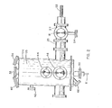
- FIG. 1 an overall view of the apparatus is given in Figure 1, which apparatus includes a reactor 10 having a pyrometer 12 mounted on an appropriate stand 11. A plurality of gas input lines 14 extend between a supply and control station 28 and reactor 10.
- Reactor 10 includes a pair of ports 16 and 18 for gaining access to the interior of the reactor as will be discussed in greater detail hereinbelow.
- a gate valve generally designated by reference numeral 20 is interposed between port 18 and reactor 10.
- reactor 10 is mounted on a supporting surface S and a pair of rotary pumps 22, 24 along with a turbo pump 25 are mounted below surface S in a cabinet generally designated by reference character C.
- a pressure gauge 26 is mounted on the side of reactor 10 for reading of the interior pressure.
- Supply and control station 28, mounted in a suitable cabinet designated by reference character C includes a visual status display portion 30 and a computer control system 32. As will be discussed hereinbelow, mounted interiorly of the station are various supply systems.
- Reactor 10 includes a cylindrical wall 34, preferably formed of a stainless steel material, which defines a growth chamber 35.
- a plurality of ports for various purposes.
- Port 36 provides access for the gas input lines 14;
- port 38 provides access for pyrometer 12 to read the temperature of the substrate;
- port 40 provides access for heating means such as a light source heating;
- port 44 provides access to inspect the substrate and deposition of material thereon;
- port 46 also provides visual access for the transfer of the substrate as will be discussed hereinbelow;
- port 48 provides access for pump unit 24; and
- port 50 is located at the base of reactor 10.
- the apparatus includes a vertical feed arm 51 and a horizontal feed arm 52.
- horizontal feed arm 52 brings the substrate/pedestal from a position at port 18 to a position adjacent port 46.
- Vertical feed arm 51 is then adapted to take the substrate/pedestal to a position proximate port 44 where it will be heated and exposed to the gaseous atmosphere for deposition of the desired coating. It will be understood that the control arms and associated transfer mechanism are normal commercial items.
- heating means are used to heat the substrate.
- RF heating which is utilized in conjunction with pyrometer 12 for controlling the substrate temperature.
- the pedestal (not shown) is desirably spaced a distance from walls 34 of growth chamber 35. It has been found that adequate spacing is desirable for most efficient operation of the apparatus. In practice, growth chamber 35 may have a diameter of 12 inches which would be suitable for a wafer having a 4 inch dimension.
- the system incorporates an inlet port 18 through which the substrate may be placed on the pedestal within an ante-chamber 37.
- Ante-chamber 37 is, however, isolated from growth chamber 35 by means of gate valve 20.
- Ante-chamber 37 has a port 54 in communication with pumps 22 for evacuating the chamber. Thus, the contamination of the interior of grc t: chamber 35 is minimized.
- supply and control station 28 includes on a first level a control computer 32 which consi l s of the computer 58 with associated display screen 56.
- a standard card arrangement 60 with interface 62 interconnects t visual status display board 30.
- the overall system may include a manual valve operator generally designated by reference numeral 57.
- Station 28 On a further level of supply and control station 28 are mounted supplies of organometallic material 66 with inlet and outlet lines 68 and 70 operatively connected thereto. Station 28 further includes appropriate air valve lines 72 and vacuum lines 74.
- reference numeral 76 designates a valve.
- reference numeral 78 designates a valve.
- a line 80 brings a suitable carrier gas such as hydrogen to a hydrogen purifier generally designated by reference numeral 82.
- a further purging line 84 is provided.
- the system will include a plurality of mass flow meter valves generally designated by reference numeral 86 for controlling the amount of material fed to input lines 14. It will be noted that mass flow meter valves 86 are, in the case of the organometallics, located between the source of organometallic and the growth chamber.
- those constituent materials available in a normal gaseous form may flow through lines 78, mass flow meter valves 86, to lines 14.
- the organometallic materials will have a carrier gas such as hydrogen passed therethrough and subsequently through mass flow meter valves 86 to input lines 14. It will be noted from the interconnections that the system may readily be purged using purging line 84 and vacuum line 74 with appropriate stop valves 76 providing for a great flexibility of operation.
- FIG. 5 is a schematic of the pumping system associated with the device.
- reference numberal 88 generally indicates a stop valve while reference numeral 90 indicates valves on a line to a source of argon back fill for use with the system.
- the system is flexible and permits the use of turbo pump 25 in association with pump 24 if desired.
- a four line trap 93 is provided with line 92 leading to charcoal drum filter 94.
- the system may include pre and post-treatment stations.
- treatments such as with an ion beam etcher in the system.
- a molecular ratio of the arsine to gallium is kept relatively low and in particular, that the molecular ratio be between 1 and 10.
- the ratio is at the lower end of the scale, one can grow a P type layer and at the higher end, one can grow an N type layer.
- thermocontrol means will be provided for maintaining the temperature of the organometallic materials at a desired value; the temperature control means will desirably be controlled by the computer in its fully automatic mode.
Landscapes
- Chemical & Material Sciences (AREA)
- General Chemical & Material Sciences (AREA)
- Chemical Kinetics & Catalysis (AREA)
- Engineering & Computer Science (AREA)
- Materials Engineering (AREA)
- Metallurgy (AREA)
- Organic Chemistry (AREA)
- Mechanical Engineering (AREA)
- Inorganic Chemistry (AREA)
- Crystallography & Structural Chemistry (AREA)
- Chemical Vapour Deposition (AREA)
Applications Claiming Priority (2)
| Application Number | Priority Date | Filing Date | Title |
|---|---|---|---|
| US51732683A | 1983-07-26 | 1983-07-26 | |
| US517326 | 1983-07-26 |
Publications (2)
| Publication Number | Publication Date |
|---|---|
| EP0132408A2 true EP0132408A2 (fr) | 1985-01-30 |
| EP0132408A3 EP0132408A3 (fr) | 1986-04-16 |
Family
ID=24059350
Family Applications (1)
| Application Number | Title | Priority Date | Filing Date |
|---|---|---|---|
| EP84305048A Withdrawn EP0132408A3 (fr) | 1983-07-26 | 1984-07-25 | Procédé et appareil pour faire croítre des couches ou pour produire des revêtements sur un substrat |
Country Status (2)
| Country | Link |
|---|---|
| EP (1) | EP0132408A3 (fr) |
| JP (1) | JPS6089919A (fr) |
Cited By (7)
| Publication number | Priority date | Publication date | Assignee | Title |
|---|---|---|---|---|
| EP0209150A3 (en) * | 1985-07-19 | 1987-05-27 | Fujitsu Limited | Apparatus of metal organic chemical vapor deposition for growing epitaxial layer of compound semiconductor |
| GB2213835A (en) * | 1987-12-18 | 1989-08-23 | Gen Electric Co Plc | Deposition apparatus |
| US4888085A (en) * | 1986-09-18 | 1989-12-19 | Eastman Kodak Company | Processes for their manufacture of monolithically integrated planar lasers differing in emission wavelengths |
| US4891093A (en) * | 1986-09-18 | 1990-01-02 | Eastman Kodak Company | Processes for the manufacture of laser including monolithically integrated planar devices |
| DE3832423A1 (de) * | 1988-09-23 | 1990-03-29 | Siemens Ag | Radiales gasmischsystem |
| US5166092A (en) * | 1988-01-28 | 1992-11-24 | Fujitsu Limited | Method of growing compound semiconductor epitaxial layer by atomic layer epitaxy |
| CN109161867A (zh) * | 2018-10-11 | 2019-01-08 | 中国科学技术大学 | 可分离式真空互联系统 |
Families Citing this family (2)
| Publication number | Priority date | Publication date | Assignee | Title |
|---|---|---|---|---|
| US5780313A (en) * | 1985-02-14 | 1998-07-14 | Semiconductor Energy Laboratory Co., Ltd. | Method of fabricating semiconductor device |
| JP2890029B2 (ja) * | 1996-03-27 | 1999-05-10 | 株式会社半導体エネルギー研究所 | 被膜形成装置及び被膜形成方法 |
Family Cites Families (1)
| Publication number | Priority date | Publication date | Assignee | Title |
|---|---|---|---|---|
| US3964940A (en) * | 1971-09-10 | 1976-06-22 | Plessey Handel Und Investments A.G. | Methods of producing gallium phosphide yellow light emitting diodes |
-
1984
- 1984-07-25 EP EP84305048A patent/EP0132408A3/fr not_active Withdrawn
- 1984-07-26 JP JP59154204A patent/JPS6089919A/ja active Pending
Cited By (11)
| Publication number | Priority date | Publication date | Assignee | Title |
|---|---|---|---|---|
| EP0209150A3 (en) * | 1985-07-19 | 1987-05-27 | Fujitsu Limited | Apparatus of metal organic chemical vapor deposition for growing epitaxial layer of compound semiconductor |
| US4883020A (en) * | 1985-07-19 | 1989-11-28 | Fujitsu Limited | Apparatus of metal organic chemical vapor deposition for growing epitaxial layer of compound semiconductor |
| US4888085A (en) * | 1986-09-18 | 1989-12-19 | Eastman Kodak Company | Processes for their manufacture of monolithically integrated planar lasers differing in emission wavelengths |
| US4891093A (en) * | 1986-09-18 | 1990-01-02 | Eastman Kodak Company | Processes for the manufacture of laser including monolithically integrated planar devices |
| GB2213835A (en) * | 1987-12-18 | 1989-08-23 | Gen Electric Co Plc | Deposition apparatus |
| GB2213835B (en) * | 1987-12-18 | 1992-07-08 | Gen Electric Co Plc | Deposition apparatus |
| US5143018A (en) * | 1987-12-18 | 1992-09-01 | The General Electric Company, P.L.C. | Apparatus for depositing uniform films by how-pressure chemical vapor deposition |
| US5166092A (en) * | 1988-01-28 | 1992-11-24 | Fujitsu Limited | Method of growing compound semiconductor epitaxial layer by atomic layer epitaxy |
| DE3832423A1 (de) * | 1988-09-23 | 1990-03-29 | Siemens Ag | Radiales gasmischsystem |
| CN109161867A (zh) * | 2018-10-11 | 2019-01-08 | 中国科学技术大学 | 可分离式真空互联系统 |
| CN109161867B (zh) * | 2018-10-11 | 2023-08-08 | 中国科学技术大学 | 可分离式真空互联系统 |
Also Published As
| Publication number | Publication date |
|---|---|
| EP0132408A3 (fr) | 1986-04-16 |
| JPS6089919A (ja) | 1985-05-20 |
Similar Documents
| Publication | Publication Date | Title |
|---|---|---|
| US6296956B1 (en) | Bulk single crystals of aluminum nitride | |
| US5254207A (en) | Method of epitaxially growing semiconductor crystal using light as a detector | |
| US6045612A (en) | Growth of bulk single crystals of aluminum nitride | |
| EP0606737A1 (fr) | Procédé et appareillage de croissance épitaxiale d'une couche de silicium, avec un contrôle des flux massiques des gaz réactifs | |
| US4388342A (en) | Method for chemical vapor deposition | |
| US6086672A (en) | Growth of bulk single crystals of aluminum nitride: silicon carbide alloys | |
| US20160160387A1 (en) | Linear Cluster Deposition System | |
| EP2038456B1 (fr) | Appareillage et procédé pour le dépôt de nitrure de gallium en grand volume | |
| JP2538042B2 (ja) | 有機金属化合物の気化供給方法とその装置 | |
| US20090223441A1 (en) | High volume delivery system for gallium trichloride | |
| US4636268A (en) | Chemical beam deposition method utilizing alkyl compounds in a carrier gas | |
| EP0506012A1 (fr) | Dispositif pour fabriquer des couches d'oxyde supraconducteur par procédé MOCVD | |
| US5463977A (en) | Method of and apparatus for epitaxially growing chemical compound crystal | |
| JPS6089919A (ja) | 基板上に層を成長しあるいは被膜を製造する方法及び装置 | |
| EP0386190B1 (fr) | Source de mercure elementaire pour deposition en phase gazeuse par procede chimique organometallique | |
| CA1325160C (fr) | Dispositif pour l'obtention d'un semi-conducteur composite | |
| US3501356A (en) | Process for the epitaxial growth of silicon carbide | |
| JP2567309B2 (ja) | 有機金属気相成長装置 | |
| US20070111372A1 (en) | Methods of forming a p-type group ii-vi semiconductor crystal layer on a substrate | |
| JPH10147871A (ja) | 気相成長装置の気化装置 | |
| JPH01261818A (ja) | 高抵抗AlGaAs混晶の気相成長方法 | |
| WO2025141430A1 (fr) | Procédé et système de croissance continue de films contenant un métal du groupe iiia | |
| JP2700210B2 (ja) | 化合物半導体の気相エピタキシャル成長法 | |
| CN119877094A (zh) | 一种兼容hvpe及mocvd工艺的氧化镓外延装置及氧化镓薄膜制备工艺 | |
| JPH01294598A (ja) | 気相成長装置 |
Legal Events
| Date | Code | Title | Description |
|---|---|---|---|
| PUAI | Public reference made under article 153(3) epc to a published international application that has entered the european phase |
Free format text: ORIGINAL CODE: 0009012 |
|
| AK | Designated contracting states |
Designated state(s): AT BE CH DE FR GB IT LI LU NL SE |
|
| PUAL | Search report despatched |
Free format text: ORIGINAL CODE: 0009013 |
|
| AK | Designated contracting states |
Kind code of ref document: A3 Designated state(s): AT BE CH DE FR GB IT LI LU NL SE |
|
| 17P | Request for examination filed |
Effective date: 19861002 |
|
| 17Q | First examination report despatched |
Effective date: 19871209 |
|
| STAA | Information on the status of an ep patent application or granted ep patent |
Free format text: STATUS: THE APPLICATION IS DEEMED TO BE WITHDRAWN |
|
| 18D | Application deemed to be withdrawn |
Effective date: 19880420 |