EP0132645A2 - Verfahren und Vorrichtung zur Erleichterung der Kollisionserkennung - Google Patents
Verfahren und Vorrichtung zur Erleichterung der Kollisionserkennung Download PDFInfo
- Publication number
- EP0132645A2 EP0132645A2 EP84107797A EP84107797A EP0132645A2 EP 0132645 A2 EP0132645 A2 EP 0132645A2 EP 84107797 A EP84107797 A EP 84107797A EP 84107797 A EP84107797 A EP 84107797A EP 0132645 A2 EP0132645 A2 EP 0132645A2
- Authority
- EP
- European Patent Office
- Prior art keywords
- bus
- bit
- collision
- information
- station
- Prior art date
- Legal status (The legal status is an assumption and is not a legal conclusion. Google has not performed a legal analysis and makes no representation as to the accuracy of the status listed.)
- Withdrawn
Links
Images


Classifications
-
- H—ELECTRICITY
- H04—ELECTRIC COMMUNICATION TECHNIQUE
- H04L—TRANSMISSION OF DIGITAL INFORMATION, e.g. TELEGRAPHIC COMMUNICATION
- H04L12/00—Data switching networks
- H04L12/28—Data switching networks characterised by path configuration, e.g. LAN [Local Area Networks] or WAN [Wide Area Networks]
- H04L12/40—Bus networks
- H04L12/407—Bus networks with decentralised control
- H04L12/413—Bus networks with decentralised control with random access, e.g. carrier-sense multiple-access with collision detection [CSMA-CD]
- H04L12/4135—Bus networks with decentralised control with random access, e.g. carrier-sense multiple-access with collision detection [CSMA-CD] using bit-wise arbitration
Definitions
- This invention pertains to a method and apparatus for transmitting data in a multiple access collision sensing mode, which facilitates detection of collisions by contending transceivers.
- the disclosures in U.S. patents US-A-4,063,220 and US-A-4,259,663 are considered representative of the state of the art in this area.
- plural transceivers may begin sending information packets on a common medium (bus) when the bus appears to be idle.
- bus common medium
- Each transceiver monitors the bus for "collision” (interference) by comparing received bits with locally transmitted bits.
- collision i.e. they immediately abort their transmissions and reschedule them; usually at relatively different times so as to reduce the likelihood of repeated collisions by the same contenders).
- a principal object of the present invention is to avoid this problem.
- Another object is to ensure reliable detection of collision in such systems by operating the station transceivers in a specifically disclosed manner.
- a further object is to operate such transceivers in a manner which not only facilitates and simplifies collision detection, but also permits performance of that function in an ancillary mode by shared user equipment whose primary function is that of logically processing data.
- a method of facilitating collision detection by contending transceivers in a multiple access data communication system in which plural transceivers having tapped connections to a common bus may simultaneously attempt to transmit packets of digital information in a bit-serial baseband form, each packet comprising multiple bit signals representing logical 1 and 0 digital information, said method being characterized in that it comprises, at each site of connection between a transceiver and the bus :
- the invention also provides :
- FIG. 1 illustrates an environmental multiple access data communication system in which the present invention may be advantageously employed.
- Bus 1 is linked at "access nodes" A, B, C, etc., to multiple transceivers 2a, 2b, 2c, etc.
- Each transceiver couples through a respective adapter --3a, 3b, 3c, etc.-- to respective user equipment comprising a general purpose computer --4a, 4b, 4c, etc.-- and peripheral attachments to the latter, indicated at 5a, 5b, 5c, etc.
- Terminating impedances 6 couple ends of the bus to ground reference potential as shown.
- Distributed capacitive coupling to ground, at each bus access node, is suggested at 9 (the effect of this capacitance and its relation to the present invention are discussed later).
- Information packet and bit signalling formats used on bus 1 are suggested, respectively, in Figures 3 and 4.
- Information is transferred between access nodes in variable length packets (also termed "frames") suggested in Figure 3.
- Each packet contains an eight-byte header section which is followed optionally by a data section varying in length from 0 to 532 bytes.
- the header section contains two address . bytes DA and OA, a control byte C, a sequence verification byte S, a two-byte count field and a two-byte "header CRC" (cyclic redundancy check) factor.
- the header bytes DA and OA indicate the destination and origin access nodes of the packet.
- the control byte C indicates the packet function and distinguishes between packets which do and do not contain data.
- the sequence verification byte S is used relative to a series of common origin packets containing related data verifying that such packets are received in the sequence of their origination.
- the count field indicates lengths of data portions in packets which contain data, and must have a value of 0 when the packet does not contain data.
- the "header CRC" is used for verifying correct reception of the header. Packets which contain data end with a two-byte data CRC which is used for verifying correct reception of the respective data.
- Figure 3 indicates the byte signalling format used on the bus 1.
- Each byte of information (header, header CRC, data or data C R C) consists of eight information (data) bit signals preceded by a start bit signal and followed by a stop bit signal.
- the stop and start signals have complementary levels, and the transition between consecutive start and stop bits provides a time reference at receiving nodes for synchronizing receivers and enabling them to sample the (eight) following information bits at correct times.
- Stop bits and "1" information bits are represented by low (ground) voltage levels on the bus.
- Start bits and "0" information bits are represented by high (positive) voltage levels on the bus.
- FIG 4 illustrates the organization of access node adapter 3a relative to the respective transceiver 2a. Since the adapter and transceiver equipments at all access nodes of the present system are generally identical, the following description will pertain to all access nodes.
- the adapter comprises an output buffer register 14, an input buffer register 15, bus access timer circuits 16 and bit/byte timing circuits 17.
- Buffer 14 is a shift register which couples data from the user equipment interface 18 to the transmitting section 19 of transceiver 2a. Data is entered into the buffer in bit-parallel byte-serial form, under control of user gating signals applied at 14.1, and shifted bit serially out to the bus 1 via OR-circuit 14.2 and transmitter 19. Timing circuits 17 insert stop and start bits between consecutive bytes via line 17.1.
- Buffer 15 performs a reverse signal to parallel conversion on the information portions of bytes in transit from the receiving section 20 of transceiver 2a to the user equipment (the stop and start elements, as noted previously, are used only for synchronizing the information bit reception timing and otherwise ignored).
- timing circuits 17 provide bit clocking signals CLK which operate through AND gate 21 to sample the information bit portions of each arriving byte into buffer 15.
- Circuits 17 also supply shift signals SH to buffers 14 and 15 for their respective shifting operations.
- circuits 17 signal a ready condition (RDY) at interface 18, via line 24, causing the user equipment to receive or issue a byte. Transfers to the user are controlled by user gating signals applied at 15.1.
- Transmission operation is supervised by the user computer via transmission enabling control signal E/T presented at 23.
- E/T is applied to the sending section 19 of the transceiver.
- Access timing circuits 16 cooperate with transition detecting circuits 17.2 in timer 17 to determine the state of the bus. If the bus is at the idle level (the level associated with stop signal transfer) for a predetermined interval longer than the time allotted for byte transfer, circuits 16 present a Bus Available indication BA to the user equipment via line 25. If BA is active and the user equipment is ready to send a packet, E/T is turned on and the transmission is immediately started. When the bus undergoes a transition from idle to active condition (i.e. from stop to start), timer 16 is reset and BA is deactivated if it was previously active.
- the adapter When BA is active and a bus transition is detected by circuits 17.2, the adapter effectively recognizes this is as indicating the start of a remote packet transfer on the bus, and presents an interruption signal I to the user processor via line 26.
- the user processor then interrupts its current processing task, examines the leading destination address byte transferred to it via buffer 15, and selectively controls reception of the full packet from the bus if the packet is approximately addressed.
- Access timer is also resettable by external reset signals XR transferrable from the user computer via line 27.
- the operation of the foregoing environment system is fully described in co-pending European patent application No—........
- the byte transfer intervals on the bus are tailored to operating characteristics of the user computers, so that the user computers can be shared for performing functions related in real time to each byte transfer in time coordination with the transfer action at the bus interface; e.g. calculation of a running check residue, updating of byte storage addresses, etc.
- the subject invention concerns the technique used presently for bit signalling and its effect on the detectability of collisions.
- each subject transceiver is conditioned to present a high impedance relative to the bus during a major portion of each "1" bit transmission interval. This is done so that local origin bit transmissions do not overpower or obscure potentially colliding bit signals originated at remote access nodes (the latter being more or less attenuated depending on the lengths of their transfer paths on the bus).
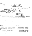
- Figure 5 is a schematic of a three-state driver circuit used in the present transmitting section 19, and Figure 6 is a truth table indicating states of operation of that circuit.
- Figure 7 diagrams the operations of the same circuit during specific bit transfers to the bus.
- Figure 8 diagrams operations of the respective receiver, adapter and user system while the circuit of Figure 5 is being operated to transfer the first two bytes of a locally originated packer (bytes DA and OA, Figure 2) to the bus.
- Figure 9 illustrates a specific bus interference condition between a local transmitter and a remote transmitter which would cause the local user computer to sense a collision.
- Figure 10 illustrates another specific bus interference condition which would be transparent only to the local user system and not affect the reception integrity of the packet locally being transmitted, but appears as a collision to user systems at all remote interfering nodes.
- the subject three-state driver circuit ( Figure 5) is connected between positive supply voltage V CC and ground reference potential. It receives data and start-stop inputs (from OR circuits 14.2, figure 2) at 30, and control inputs G1 and G2 at 31 and 32, respectively. Its output at 33 passes to the bus. As shown in Figure 6, the circuit presents a high impedance Z/H to the bus when either of its control inputs is at a logical 1 level, and actively transfers a high/V or low/ground voltage condition functionally related to its data input when both G1 and G2 are at logical 0 levels (recall from Figure 3 that the high voltage condition is transferred to represent 0 data and start bits, and the low voltage condition is used to represent 1 data and stop bits).
- Figure 7 shows that during the output transfer of either a 1 data bit or a stop bit, the subject circuit is operated initially for a brief period of time t to actively transfer a 1 output voltage level (i.e. by conditioning Gl and G2 jointly to 0 levels for that period), and subsequently for the remainder of the bit transfer period in the high impedance (isolated) state.
- the brief period of active signal transfer is sufficient to permit the bus to quickly discharge charges previously accumulated at the local site of connection (site A) -- compared to the passive discharge time 50 -- and quickly reach the desired ground voltage level, assuming no interference by a remote sender.
- site A site of connection
- it is also sufficiently short to preclude damage to the driver circuits by an interfering signal on the bus (applying undesired back currents).
- Figure 7 also shows that during transfer of a 0 data bit or start bit to the bus, the driver circuit is operated to actively couple a V CC level to the bus. It should be noted that the rate of passive decay of charges accumulated on the bus (through the bus and its distributed capacitance), when all access node drivers are in the isolated state, is much slower than the rate associated with active charging or discharging through the driver circuits. Hence, the bus level established during the brief period of active coupling within each bit transfer period does not vary substantially during the remainder of the transfer period.
- Figure 8 shows that while the adapter at an access node is sending the first two bytes of a packet to the bus (i.e. the destination and origin address bytes DA and OA, Figure 2), its receiver samples the bus level under control of its receive clock (R -J, and shifts the bits representing those levels into its receiving byte buffer 15. Bytes accumulated in buffer 15 are passed to the local user computer by the action of AND circuit 91 and gate bank 15a. The user computer compares the received bytes to copies of the transmitted bytes which it has saved, and declares a collision if they do not match. This function is performed by the computer before it transfers the next outgoing byte (to shift buffer 14, Figure 4).
- the outgoing transfer is immediately terminated (aborted) and scheduled for deferred repetition. If a collision is not declared, the outgoing byte transfer process is continued, and if the second byte of the local origin packet has been sent, the local receiver and collision monitoring function may be disabled.
- Figure 8 notes that during the period of collision monitoring (while the first two bytes of the local packet are being sent), the local system (node A adaptor) reacts differently to the presence of interfering bit transfer conditions on the bus.
- the local system at the A access site is sending a 0 bit and a remote system is sending a 1 bit
- the local receiver will transfer a 0 bit level (to buffer 15, Figure 4) when its bit sampling function is enabled.
- the local receiver will sample a 0. Consequently, the bit information acquired by the local receiver will differ from the corresponding outgoing bit only when the outgoing bit is a 1 and a remote system is sending a 0.
- the local driver initially couples the bus to ground through its internal conductive path while the remote driver is charging the bus to a positive level through its internal resistive path (again, see Figure 5).
- the local effect is to clamp the bus to ground potential initially, but then the bus charges quickly to a positive level which it sustains after the local driver goes into the high impedance state.
- the level is sufficient to be sampled as a 0 when the sampling function of the local receiver is next enabled.
- each access node has a unique address different from all other nodes, and the byte representing that address must contain at least one 1 bit. Furthermore, the byte transfer period presently employed is long by comparison to the maximal propagation delay between access nodes. Consequently, a high likelihood exists that the effects of interference would be manifest at all nodes during the transfer of the second packet byte (i.e. the origin address function OA), and this likelihood is strengthened by the extension of the collision monitoring function to span the transfers of both the first and second bytes of each packet.
- Figures 9 and 10 illustrate exemplary pairs of local and remote O A byte value transmissions which would and would not give rise to local declarations of collision. From these examples, it should be appreciated that when interference is present on the bus but not locally perceived (at the A access site) as a collision ( Figure 10), the same conditions would cause the receivers at the remote sending sites to detect collision (since they would be sending 1's interference with 0's from the A site).
- the 0 bits in the local origin DA and OA byte transfers would produce 0 levels on the bus regardless of any contemporary interferences, and therefore be perceived at all node receivers as 0 bits; and the 1 bits sent from a node which does not perceive collision must either enter the bus free of interference or in interference only with 1 bits being sent by other nodes (i.e. in interference but not in collision conflict). Therefore, in each instance where two or more access nodes attempt to access the bus simultaneously, and at least one of them does not perceive a collision, the first two bytes sent by the latter node will be seen in their original form at all other nodes.
Landscapes
- Engineering & Computer Science (AREA)
- Computer Networks & Wireless Communication (AREA)
- Signal Processing (AREA)
- Small-Scale Networks (AREA)
Applications Claiming Priority (2)
| Application Number | Priority Date | Filing Date | Title |
|---|---|---|---|
| US51817583A | 1983-07-28 | 1983-07-28 | |
| US518175 | 1983-07-28 |
Publications (2)
| Publication Number | Publication Date |
|---|---|
| EP0132645A2 true EP0132645A2 (de) | 1985-02-13 |
| EP0132645A3 EP0132645A3 (de) | 1987-10-28 |
Family
ID=24062884
Family Applications (1)
| Application Number | Title | Priority Date | Filing Date |
|---|---|---|---|
| EP84107797A Withdrawn EP0132645A3 (de) | 1983-07-28 | 1984-07-05 | Verfahren und Vorrichtung zur Erleichterung der Kollisionserkennung |
Country Status (2)
| Country | Link |
|---|---|
| EP (1) | EP0132645A3 (de) |
| JP (1) | JPS6043942A (de) |
Cited By (2)
| Publication number | Priority date | Publication date | Assignee | Title |
|---|---|---|---|---|
| EP0275464A1 (de) * | 1986-12-11 | 1988-07-27 | Siemens Nixdorf Informationssysteme Aktiengesellschaft | Sende-Empfangs-Einrichtung für ein Busleitungssystem |
| US6483847B1 (en) | 1998-12-01 | 2002-11-19 | Koninklijke Philips Electronics N.V. | Arbitration scheme for a serial interface |
Families Citing this family (1)
| Publication number | Priority date | Publication date | Assignee | Title |
|---|---|---|---|---|
| US4821258A (en) * | 1986-08-06 | 1989-04-11 | American Telephone And Telegraph Company At&T Bell Laboratories | Crosspoint circuitry for data packet space division switches |
Family Cites Families (4)
| Publication number | Priority date | Publication date | Assignee | Title |
|---|---|---|---|---|
| JPS5619144B2 (de) * | 1973-12-04 | 1981-05-06 | ||
| US4186379A (en) * | 1977-04-28 | 1980-01-29 | Hewlett-Packard Company | High-speed data transfer apparatus |
| NL8005458A (nl) * | 1980-10-02 | 1982-05-03 | Philips Nv | Kommunikatiesysteem en station geschikt hiervoor. |
| FR2507415A1 (fr) * | 1981-06-05 | 1982-12-10 | Ryckeboer Christian | Procede et dispositif pour la communication serie asynchrone de type multipoints de plusieurs emetteurs-recepteurs logiques |
-
1984
- 1984-04-20 JP JP7879284A patent/JPS6043942A/ja active Pending
- 1984-07-05 EP EP84107797A patent/EP0132645A3/de not_active Withdrawn
Cited By (3)
| Publication number | Priority date | Publication date | Assignee | Title |
|---|---|---|---|---|
| EP0275464A1 (de) * | 1986-12-11 | 1988-07-27 | Siemens Nixdorf Informationssysteme Aktiengesellschaft | Sende-Empfangs-Einrichtung für ein Busleitungssystem |
| US4888764A (en) * | 1986-12-11 | 1989-12-19 | Siemens Aktiengesellschaft | Transmission-reception equipment for a bus system |
| US6483847B1 (en) | 1998-12-01 | 2002-11-19 | Koninklijke Philips Electronics N.V. | Arbitration scheme for a serial interface |
Also Published As
| Publication number | Publication date |
|---|---|
| EP0132645A3 (de) | 1987-10-28 |
| JPS6043942A (ja) | 1985-03-08 |
Similar Documents
| Publication | Publication Date | Title |
|---|---|---|
| US4539677A (en) | Multiple access data communication system | |
| US4542380A (en) | Method and apparatus for graceful preemption on a digital communications link | |
| EP0525985B1 (de) | Hochgeschwindigkeitschnittstelle für eine Duplex-Datenverbindung | |
| EP0544964B1 (de) | Vorrichtung zur Speicherung und Durchschaltung und Verfahren zur Datensicherung während der Speicherung | |
| US5400340A (en) | End of packet detector and resynchronizer for serial data buses | |
| US7328399B2 (en) | Synchronous serial data communication bus | |
| WO1983001359A1 (en) | A local area contention network data communication system | |
| US5166678A (en) | Dual master implied token communication system | |
| US5572546A (en) | Data communications system with multilink protocol | |
| US4642630A (en) | Method and apparatus for bus contention resolution | |
| EP0117677B1 (de) | Datenübertragungssysteme | |
| KR100258398B1 (ko) | 멀티프로세서 통신 시스템에서의 데이타 충돌 검출을 위한 방법 및 장치 | |
| JPH0241221B2 (de) | ||
| JPS63296540A (ja) | 単一集積回路マイクロ制御器におけるマルチプロトコル通信制御器 | |
| EP0602806A2 (de) | HDLC-Empfänger | |
| EP0439646B1 (de) | System und Protokoll für ein optisches Sternnetz mit minimaler Verzögerung zwischen aufeinanderfolgenden Datenpaketen | |
| JP3709289B2 (ja) | データ再送を実行するデータ送受信装置及び並列プロセッサシステム | |
| EP0893019B1 (de) | Verfahren und schnittsstellenschaltung für multiplex-kommunikation | |
| US4191941A (en) | Switch matrix for data transfers | |
| EP0132645A2 (de) | Verfahren und Vorrichtung zur Erleichterung der Kollisionserkennung | |
| CN116185936A (zh) | 一种spi通信数据收发异常检测控制系统及检测方法 | |
| EP1051821B1 (de) | Arbitrierungsschema für ein serielles Interface | |
| US6643816B1 (en) | Transmitting apparatus and error handling method in transmitting apparatus | |
| WO2002008912A2 (en) | Ground level shift detection in can systems | |
| JP2643089B2 (ja) | 並列/直列バスにおけるエラー検出および回復システム |
Legal Events
| Date | Code | Title | Description |
|---|---|---|---|
| PUAI | Public reference made under article 153(3) epc to a published international application that has entered the european phase |
Free format text: ORIGINAL CODE: 0009012 |
|
| 17P | Request for examination filed |
Effective date: 19841123 |
|
| AK | Designated contracting states |
Designated state(s): DE FR GB |
|
| PUAL | Search report despatched |
Free format text: ORIGINAL CODE: 0009013 |
|
| AK | Designated contracting states |
Kind code of ref document: A3 Designated state(s): DE FR GB |
|
| 17Q | First examination report despatched |
Effective date: 19890712 |
|
| STAA | Information on the status of an ep patent application or granted ep patent |
Free format text: STATUS: THE APPLICATION IS DEEMED TO BE WITHDRAWN |
|
| 18D | Application deemed to be withdrawn |
Effective date: 19900123 |
|
| RIN1 | Information on inventor provided before grant (corrected) |
Inventor name: CHANG, YUAN |