EP0132885B1 - Multipliziererschaltung, die Schaltungen mit geschalteten Kapazitäten enthält - Google Patents
Multipliziererschaltung, die Schaltungen mit geschalteten Kapazitäten enthält Download PDFInfo
- Publication number
- EP0132885B1 EP0132885B1 EP84201044A EP84201044A EP0132885B1 EP 0132885 B1 EP0132885 B1 EP 0132885B1 EP 84201044 A EP84201044 A EP 84201044A EP 84201044 A EP84201044 A EP 84201044A EP 0132885 B1 EP0132885 B1 EP 0132885B1
- Authority
- EP
- European Patent Office
- Prior art keywords
- signal
- circuit
- pulse
- multiplying
- capacitor
- Prior art date
- Legal status (The legal status is an assumption and is not a legal conclusion. Google has not performed a legal analysis and makes no representation as to the accuracy of the status listed.)
- Expired
Links
- 239000003990 capacitor Substances 0.000 title claims description 48
- 238000005070 sampling Methods 0.000 claims description 9
- 230000000737 periodic effect Effects 0.000 claims description 4
- 238000010586 diagram Methods 0.000 description 6
- 238000010276 construction Methods 0.000 description 5
- 238000001228 spectrum Methods 0.000 description 5
- 239000011159 matrix material Substances 0.000 description 2
- 230000004048 modification Effects 0.000 description 2
- 238000012986 modification Methods 0.000 description 2
- 230000000694 effects Effects 0.000 description 1
- 230000012447 hatching Effects 0.000 description 1
- 238000000034 method Methods 0.000 description 1
Images


Classifications
-
- H—ELECTRICITY
- H03—ELECTRONIC CIRCUITRY
- H03D—DEMODULATION OR TRANSFERENCE OF MODULATION FROM ONE CARRIER TO ANOTHER
- H03D1/00—Demodulation of amplitude-modulated oscillations
- H03D1/22—Homodyne or synchrodyne circuits
-
- H—ELECTRICITY
- H03—ELECTRONIC CIRCUITRY
- H03H—IMPEDANCE NETWORKS, e.g. RESONANT CIRCUITS; RESONATORS
- H03H19/00—Networks using time-varying elements, e.g. N-path filters
-
- H—ELECTRICITY
- H03—ELECTRONIC CIRCUITRY
- H03C—MODULATION
- H03C1/00—Amplitude modulation
-
- H—ELECTRICITY
- H03—ELECTRONIC CIRCUITRY
- H03H—IMPEDANCE NETWORKS, e.g. RESONANT CIRCUITS; RESONATORS
- H03H17/00—Networks using digital techniques
-
- H—ELECTRICITY
- H03—ELECTRONIC CIRCUITRY
- H03H—IMPEDANCE NETWORKS, e.g. RESONANT CIRCUITS; RESONATORS
- H03H19/00—Networks using time-varying elements, e.g. N-path filters
- H03H19/004—Switched capacitor networks
Definitions
- the invention relates to a multiplying circuit for multiplying a first signal x(t) by a periodic second signal y(t). It is particularly suitable for use as an amplitude demodulator in a stereo decoder or in a phase-locked loop (PLL) and comprises circuits constructed with switched capacitors.
- PLL phase-locked loop
- an amplitude demodulator has for its function to convert a band-limited signal s(nf o ; t) whose frequency spectrum is located in a frequency band extending from the frequency (nf o -f 1 )Hz to a frequency (nf+f,)Hz, into an AF-signal x(n; t) whose frequency spectrum is located in the frequency band extending from the frequency 0 Hz to the frequency f 1 Hz.
- the last-mentioned frequency band will be called AF-band (Audio Frequency band) hereinafter.
- f o and f 1 are a fixed frequency and n is an integer.
- the amplitude demodulator comprises a what is commonly denoted as a pre-modulation filter to which x'(t) is applied and which converts it into a signal x(t) which comprises only a limited number, for example N, of these band-limited signals.
- each of these band-limited signals can be written as:
- x(t) is multiplied by a periodic carrier signal y(t) which satisfies, for example, the expression:
- a product signal z(t) is obtained which in addition to the AF-signal x(1; t) located in the AF band comprises N-2 further signals located around multiples of the frequency f o .
- this signal z(t) is now applied to a post-modulation filter both signals located around these multiples of f o can be suppressed so that this filter supplies the AF-signal z(1; t) as an output signal.
- a carrier signal which in contrast to the above mentioned sinusoidally varying carrier signal is not amplitude-continuous but which is amplitude-discrete and consequently can only assume a limited number of predetermined amplitude values. This may result in the carrier signal y(t) not comprising certain components whose frequencies are an integral multiple of f o , so that those signals x(nf o ; t) located around those frequencies do not arrive in the AF-band.
- each signal channel comprises, arranged in cascade with the switching circuit, a weighting network having a constant weighting factor where To represents a constant, and a pulse-reshaping circuit for converting a pulse applied thereto into a pulse whose width is not more than equal to 1/f o .
- Each signal channel supplies a channel signal consisting of a sequence of pulses whose amplitudes are equal to the product of the first signal x(t) and the constant weighting factor and whose width is determined by the pulse-reshaping circuit. The channel signals thus obtained are added together in an adder to form the desired product signal.
- each signal channel comprises a capacitor having a capacitance C(k) which together with the associated switching circuit forms part of a circuit comprising a switched capacitor.
- This last-mentioned circuit is further followed by an operational amplifier which is shunted by a capacitor having a capacitance C and functions as a pulse-reshaping circuit.
- the weighting network is formed by the series arrangement of the two capacitors and the weighting factor W(k) of this weighting network is equal to the ratio C(k)/C of the two capacitances.
- the operational amplifier and the capacitor shunting it are used in common for all signal channels and it then also functions as an adder device.
- the invention has for its object to provide a multiplying circuit in which the above-mentioned disadvantages are eliminated to a very great extent.
- the multiplying circuit therefore comprises:
- the sampling circuit produces samples of the sum signal, the value of these samples being independent of the duration of the control pulses, so that these pulses may again be considered as delta pulses. Since the sampling pulses occur after the ends of the control pulses and as at that moment the capacitors of the different switched-capacitor circuits are no further charged, the amplitude values of the samples of the sum signal are independent of mutually different charging time constants in the different signal channels.
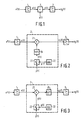
- an amplitude demodulator generally comprises a premodulation filter 1, a multiplying circuit 2 and a post-modulation filter 3.
- a signal x'(t) which is filtered and converted into the first signal x(t) is applied to the pre-modulation filter 1.
- This product signal is filtered by the post-modulation filter 3 which thus produces as an output signal z o (t) which is, for example, equal to the above-mentioned AF-signal x(1; t).
- the first signal x(t) represents, for example, the what is commonly referred to as the stereo multiplex signal which is defined by the expression:
- L(t) is the left-hand signal
- R(t) is the right-hand signal.
- the frequency f o is usually equal to 38 kHz.
- the sum signal L(t)+R(t) can be separated from the stereo multiplex signal x(t) with the aid of a low-pass filter. If this sum signal is applied in known manner together with the difference signal L(t)-R(t) to a matrix circuit, then this matrix circuit produces the left-hand signal L(t) and the right-hand signal R(t) separate from each other.
- Reference 1 describes that it is advantageous to construct the multiplying circuit 2 in the manner as shown schematically in Fig. 2, or in Fig. 3.
- These embodiments each comprise a multiplier 21, a clock pulse generator 22 producing a series of delta pulses g(t) at a rate equal to which are applied as sampling pulses to a sampling circuit 23 in which the carrier signal y(t) is sampled and which thus produces a sampled version y(t) of this carrier signal.
- this signal y(t) is applied to the multiplier 21 via a pulse-reshaping circuit 24.
- This multiplying circuit thus produces a product signal z 1 (t).
- this signal y(t) is applied directly to the multiplier 21.
- this multiplying circuit comprises a pulse-reshaping circuit 25 which is here connected to the output of the multiplier 21, so that this multiplying circuit produces the product signal z 2 (t).
- the pulse-reshaping circuit 24 has an impulse response h 1 (t) and that the pulse-reshaping circuit 25 has an impulse response h 2 (t).
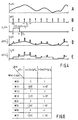
- Fig. 4A shows a portion of the first signal x(t)
- Fig. 4B shows the train of delta pulses g(t) generated by the clock pulse generator 23.
- the embodiment shown in Fig. 3 is perfectly suitable for construction for a stereo decoder, with the aid of circuits comprising switched capacitors.
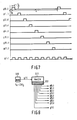
- This multiplying circuit comprises N signal channels 26(.).
- the signal channels 26(0)-26(4) receive the first signal x(t) and the signal channels 26(5)-26(7) receive the signal -x(t) which represents the polarity-inverted version of x(t). This polarity inversion is effected by an inverter circuit 27.
- Each signal channel comprises a switching circuit formed by the two switches 28(k, 1) and 28(k, 2) which are controlled by control pulses g(k; i).
- a capacitor 29(k) which has a capacitance C(k) is arranged between these two switches. In conjunction with the two switches this capacitor forms a so-called “switched capacitor circuit”.
- This circuit is further followed by an operational amplifier 30 which is shunted by a capacitor 31 having capacitance C and is used in common by all signal channels.
- this operational amplifier 30 operates together with this capacitor 31 for each signal channel as a pulse-reshaping circuit which converts a pulse produced by the switched capacitor circuits into a pulse of a length NT s and, in addition, this amplifier operates as an adder adding all these pulses together. More specifically, the contribution of the signal channel having number k to the output voltage of the operational amplifier 30 is equal to Herein x[g(k; i)] represents the value of the signal x(t) at the instant at which the control pulse g(k; i) occurs. The quotient C(k)/C represents the weighting factor W(k) which is characteristic of the relevant signal channel.
- the control pulses g(k; i) are generated by the pulse generator circuit 32 and that in such a way that as shown in Fig. 7 those control pulses g(k; i) which are applied to the switches 28(k, 1) and 28(k, 2) occur with a repetition rate
- it comprises a modulo-2N counter 321 and a decoding network 322 connected thereto.
- Each time the counting position 0000 occurs a control pulse g(0, t) is produced. If the counting position is 0010 then a control pulse g(1, t) is produced and each time the counting position is 0100 a control pulse g(2, t) is produced, etc. No control pulse is produced at any odd value of the counting position.
- Fig. 5 must be considered as a practical embodiment of the multiplying circuit shown schematically in Fig. 3.
- the signal z(t) produced by the operational amplifier 30 must be identical to the signal z 2 (t) such as it is produced by the pulse reshaping circuit 25 (see Fig. 3).
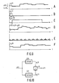
- the multiplying circuit 2 shown in Fig. 3 produces in response to the signal x(t) shown in Fig. 4A the product signal Z2 (t) whose shape is shown in Fig. 9A.
- the switches 28(., .) have a certain resistance and a certain time is required to charge the capacitor 29(.) (charging time constants) to a voltage equal to the instantaneous value of x(t).
- the control pulses g(., i) have a measurable width. In this embodiment this width has been chosen equal to T s /2.
- Multiplying circuit 221 is then of the construction shown in Fig. 3.
- the signal x(t) is applied to both multiplying circuits and the product signals z 1 (t) and z 2 (t), respectively produced by these multiplying circuits are added together in an adder device 33 whereby the signal z(t) produced by the operational amplifier 30 is obtained.
- the impulse response h l (t) then has the pulse shape shown in Fig.
- a further switched-capacitor circuit is connected to the output of the operational amplifier 30, the circuit being formed by the two switches 34(1) and 34(2) and the capacitor 35 having a capacitance C(8).
- the switches 34(.) each have a switching position a and a switching position b and are controlled by the control pulses g'(i) shown in Fig. 7 and occurring with a period Ts, a duration of, for example, T s /2 and each coinciding with a control pulse g(k, i).
- these control pulses are also produced by the pulse generator circuit 32. More specifically such a control pulse occurs each time the counting position of modulo-2N counter is even.
- the output of switch 34(2) is preferably connected to the input of an operational amplifier 36, which is shunted by a capacitor 37 having a capacitance C(9) and which thus produces the signal Z2 (t).
- this switched-capacitor circuit 34(.), 35 conveys a certain signal value to the operational amplifier 36, namely only that signal value z(t) had at the end of the control pulse g'(i)
- this switched-capacitor circuit represents a sampling arrangement which is controlled by the control pulses g'(i). More specifically, the signal z(t) is sampled each time a trailing edge of a control pulse g'(i) occurs. To obtain the signal shown in Fig. 9A this trailing edge must generally speaking, be located in an interval of which several are shown in Fig. 9E by means of hatching. Each interval is located between the end of a control pulse g(k, i) and the beginning of the subsequent control pulse g(k+1, i).
- capacitor 37 is shunted by a switch 38 which is also controlled by the control pulses g(i) and one pole of which is connected to ground potential via a capacitor 39 having capacitance C(9).
- switch 38 is in the switching position a and capacitor 39 is charged to the same voltage as to which capacitor 37 has been charged. If no control pulse g'(i) is produced, then switch 38 is adjusted to the switching position b, causing capacitor 39 to convey its charge to capacitor 37 which is first discharged thereby and is thereafter charged by the charge conveyed from capacitor 35 to capacitor 37.
Landscapes
- Engineering & Computer Science (AREA)
- Power Engineering (AREA)
- Stereo-Broadcasting Methods (AREA)
- Filters That Use Time-Delay Elements (AREA)
- Digital Transmission Methods That Use Modulated Carrier Waves (AREA)
- Manipulation Of Pulses (AREA)
Claims (5)
- Multiplizierschaltung zum Multiplizieren eines ersten Signals x(t) mit einem periodischen zweiten Signal y(t), mit:A) einem Multiplizierschaltungseingang zum Empfangen des ersten Signals x(t) und einem Multiplizierschaltungsausgang zum Liefern eines Produktsignals;B) N Signalkanälen, die je mit dem Multiplizierschaltungseingang zum Empfangen des ersten Signals verbunden sind, die je ein Kanalsignal liefern und die je die folgenden Elemente aufweisen:Ba) eine Schaltungsanordnung mit einer geschalteten Kapazität, wobei die Schaltungsanordnung, die in den Signalkanal mit der Nummer k aufgenommen ist, von einer Reihe von Steuerimpulsen g(k, i) gesteuert wird, die je eine endliche Dauer haben und wobei k=0, 1, 2, ... N-1 und i=-2, -1, 0, 1, 2, 3, ... ist.Bb) Mittel zum Multiplizieren der Amplitude des empfangenen ersten Signals x(t) mit einem konstanten Gewichtungsfaktor W(k), der dem Wert
 Bc) Impulsreformmittel, die mit der genannten Schaltungsanordnung in Reihe geschaltet sind zum Umwandeln eines derselben zugeführten Impulses in einem Impuls mit einer vorbestimmten Dauer.C) Mittel zum Addieren der N Kanalsignale zum Erzeugen eines Summensignals;D) einer Abtastschaltungsanordnung zum Abtasten des Summensignals zu Zietpunkten, die innerhalb des Intervalls zwischen dem Ende eines Steuerimpulses g(k, i) und dem Anfang des Steuerimpulses g(k+1, i) liegen und deren Ausgang mit dem Ausgang der Multiplizierschaltung gekoppelt ist;E) einer Impulsgeneratorschaltung zum Erzeugen der Steuerimpulsreihe g(k, i), wobei diese Impulse mit einer Wiederholungsperiode To und zu Zeitpunkten
Applications Claiming Priority (2)
| Application Number | Priority Date | Filing Date | Title |
|---|---|---|---|
| NL8302591A NL8302591A (nl) | 1983-07-20 | 1983-07-20 | Vermenigvuldigschakeling met geschakelde capaciteiten circuits. |
| NL8302591 | 1983-07-20 |
Publications (2)
| Publication Number | Publication Date |
|---|---|
| EP0132885A1 EP0132885A1 (de) | 1985-02-13 |
| EP0132885B1 true EP0132885B1 (de) | 1987-03-25 |
Family
ID=19842183
Family Applications (1)
| Application Number | Title | Priority Date | Filing Date |
|---|---|---|---|
| EP84201044A Expired EP0132885B1 (de) | 1983-07-20 | 1984-07-12 | Multipliziererschaltung, die Schaltungen mit geschalteten Kapazitäten enthält |
Country Status (7)
| Country | Link |
|---|---|
| US (1) | US4616185A (de) |
| EP (1) | EP0132885B1 (de) |
| JP (1) | JPS6041804A (de) |
| KR (1) | KR850001645A (de) |
| DE (1) | DE3462839D1 (de) |
| HK (1) | HK35588A (de) |
| NL (1) | NL8302591A (de) |
Families Citing this family (21)
| Publication number | Priority date | Publication date | Assignee | Title |
|---|---|---|---|---|
| NL8502071A (nl) * | 1985-07-18 | 1987-02-16 | Philips Nv | Vermenigvuldigschakeling van het geschakelde capaciteiten type. |
| US4786863A (en) * | 1985-12-23 | 1988-11-22 | General Electric Co. | Solid state watthour meter with switched-capacitor integration |
| US4727333A (en) * | 1986-06-30 | 1988-02-23 | Rca Corporation | Circuitry for multiplying a PCM signal by a sinusoid |
| US4789837A (en) * | 1987-04-22 | 1988-12-06 | Sangamo Weston, Inc. | Switched capacitor mixer/multiplier |
| US5182521A (en) * | 1987-08-28 | 1993-01-26 | The University Of Melbourne | Time-multiplexed switched capacitor circuit having reduced capacitance |
| WO1989006069A1 (en) * | 1987-12-24 | 1989-06-29 | The University Of Melbourne | Switched capacitor circuits |
| FR2641924B1 (fr) * | 1988-12-28 | 1991-05-03 | Sgs Thomson Microelectronics | Generateur de forme d'onde de signal analogique |
| US5039870A (en) * | 1990-05-21 | 1991-08-13 | General Electric Company | Weighted summation circuits having different-weight ranks of capacitive structures |
| US5039871A (en) * | 1990-05-21 | 1991-08-13 | General Electric Company | Capacitive structures for weighted summation as used in neural nets |
| JP2579569B2 (ja) * | 1991-12-03 | 1997-02-05 | クラリオン株式会社 | Daコンバータ |
| US5666080A (en) * | 1993-06-17 | 1997-09-09 | Yozan, Inc. | Computational circuit |
| US5617053A (en) * | 1993-06-17 | 1997-04-01 | Yozan, Inc. | Computational circuit |
| CN1109404C (zh) * | 1993-09-20 | 2003-05-21 | 株式会社鹰山 | 计算电路 |
| JPH08204567A (ja) * | 1995-01-31 | 1996-08-09 | Canon Inc | 半導体装置とこれを用いた半導体回路、相関演算装置、a/d変換器、d/a変換器及び信号処理システム |
| US5659269A (en) * | 1995-03-13 | 1997-08-19 | Harris Corporation | Zero phase error switched-capacitor phase locked loop filter |
| DE69611768T2 (de) * | 1995-04-26 | 2001-05-31 | Sharp Kabushiki Kaisha, Osaka | Multiplizierschaltung |
| US6452424B1 (en) | 1999-09-28 | 2002-09-17 | Conexant Systems, Inc. | Method and apparatus for multiple channel signal processing |
| EP1959562B1 (de) * | 2007-02-15 | 2010-12-08 | STMicroelectronics Srl | Volldifferentieller Demodulator mit variabler Verstärkung und Demodulationsverfahren eines Signals |
| IT1392553B1 (it) | 2008-12-11 | 2012-03-09 | St Microelectronics Rousset | Dispositivo elettronico a capacita' variabile e dispositivo microelettromeccanico incorporante tale dispositivo elettronico |
| US8714012B2 (en) | 2010-02-16 | 2014-05-06 | Stmicroelectronics S.R.L. | Microelectromechanical gyroscope with inversion of actuation forces, and method for actuating a microelectromechanical gyroscope |
| KR101952813B1 (ko) * | 2015-04-14 | 2019-02-27 | 알프스 알파인 가부시키가이샤 | 정현파 승산 장치와 이것을 가지는 입력 장치 |
Family Cites Families (4)
| Publication number | Priority date | Publication date | Assignee | Title |
|---|---|---|---|---|
| NL154082B (nl) * | 1968-07-09 | 1977-07-15 | Philips Nv | Inrichting voor overdracht van rechthoekige synchrone informatiepulsen. |
| AT325115B (de) * | 1972-05-16 | 1975-10-10 | Siemens Ag | Anordnung zur übertragung eines amplitudenmodulierten amplitudensignals |
| US4006353A (en) * | 1975-11-21 | 1977-02-01 | Signatron, Inc. | Signal multiplier devices |
| NL8104668A (nl) * | 1981-10-14 | 1983-05-02 | Philips Nv | Vermenigvuldigschakeling voor stereo-decoders. |
-
1983
- 1983-07-20 NL NL8302591A patent/NL8302591A/nl not_active Application Discontinuation
-
1984
- 1984-06-13 US US06/630,510 patent/US4616185A/en not_active Expired - Fee Related
- 1984-07-12 DE DE8484201044T patent/DE3462839D1/de not_active Expired
- 1984-07-12 EP EP84201044A patent/EP0132885B1/de not_active Expired
- 1984-07-17 JP JP59147029A patent/JPS6041804A/ja active Pending
- 1984-07-19 KR KR1019840004255A patent/KR850001645A/ko not_active Ceased
-
1988
- 1988-05-12 HK HK355/88A patent/HK35588A/xx unknown
Also Published As
| Publication number | Publication date |
|---|---|
| KR850001645A (ko) | 1985-03-30 |
| HK35588A (en) | 1988-05-20 |
| DE3462839D1 (en) | 1987-04-30 |
| JPS6041804A (ja) | 1985-03-05 |
| EP0132885A1 (de) | 1985-02-13 |
| US4616185A (en) | 1986-10-07 |
| NL8302591A (nl) | 1985-02-18 |
Similar Documents
| Publication | Publication Date | Title |
|---|---|---|
| EP0132885B1 (de) | Multipliziererschaltung, die Schaltungen mit geschalteten Kapazitäten enthält | |
| EP0135212B1 (de) | Band-Sperr-Filter mit geschalteten Kapazitäten | |
| US8385874B2 (en) | Discrete time direct sampling circuit and receiver | |
| US4588979A (en) | Analog-to-digital converter | |
| JP3510794B2 (ja) | 信号処理装置および通信機 | |
| US6032171A (en) | Fir filter architecture with precise timing acquisition | |
| JP2004538703A (ja) | アナログfirフィルタ | |
| EP0209948B1 (de) | Multipliziererschaltung mit geschalteten Kapazitäten | |
| JPH05206957A (ja) | シグマデルタ変換器の分割フィルタ及び同前を用いるアナログ/ディジタル変換器 | |
| JPH0974364A (ja) | Fm多重受信装置 | |
| EP0077091B1 (de) | Multiplizier-Schaltung für Stereodekoder | |
| JPH03226135A (ja) | スペクトラム拡散通信用相関器 | |
| US5850161A (en) | Digital FM demodulator using pulse generators | |
| US5500613A (en) | Method for producing a digital sine wave signal with a given sampling rate, and circuit configuration for carrying out the method | |
| RU2030108C1 (ru) | Преобразователь период - напряжение | |
| US4933974A (en) | Switched capacitor pilot phase and magnitude detector | |
| EP0067824B1 (de) | Empfänger für cvsd-modulation mit integraler filterung | |
| SU1656692A1 (ru) | Приемник двоичных символов | |
| RU2013862C1 (ru) | Устройство цифровой фазовой автоматической подстройки частоты | |
| SU1058084A1 (ru) | Демодул тор фазоманипулированных сигналов | |
| RU2037959C1 (ru) | Формирователь высокочастотных сигналов с изменяющейся амплитудой | |
| SU1225039A1 (ru) | Цифровой частотный манипул тор | |
| SU995264A1 (ru) | Цифровой фазовый дискриминатор | |
| NL8402465A (nl) | Banddoorlaatfilter voor de ontvangst van een via een elektrisch energievoorzieningsnet overgedragen audiosignaal. | |
| SU1133678A1 (ru) | Дискретно-адресна система св зи |
Legal Events
| Date | Code | Title | Description |
|---|---|---|---|
| PUAI | Public reference made under article 153(3) epc to a published international application that has entered the european phase |
Free format text: ORIGINAL CODE: 0009012 |
|
| AK | Designated contracting states |
Designated state(s): DE FR GB IT |
|
| 17P | Request for examination filed |
Effective date: 19850712 |
|
| 17Q | First examination report despatched |
Effective date: 19860612 |
|
| GRAA | (expected) grant |
Free format text: ORIGINAL CODE: 0009210 |
|
| AK | Designated contracting states |
Kind code of ref document: B1 Designated state(s): DE FR GB IT |
|
| ITF | It: translation for a ep patent filed | ||
| REF | Corresponds to: |
Ref document number: 3462839 Country of ref document: DE Date of ref document: 19870430 |
|
| ET | Fr: translation filed | ||
| PLBE | No opposition filed within time limit |
Free format text: ORIGINAL CODE: 0009261 |
|
| STAA | Information on the status of an ep patent application or granted ep patent |
Free format text: STATUS: NO OPPOSITION FILED WITHIN TIME LIMIT |
|
| 26N | No opposition filed | ||
| PGFP | Annual fee paid to national office [announced via postgrant information from national office to epo] |
Ref country code: GB Payment date: 19900702 Year of fee payment: 7 |
|
| PGFP | Annual fee paid to national office [announced via postgrant information from national office to epo] |
Ref country code: FR Payment date: 19900720 Year of fee payment: 7 |
|
| ITTA | It: last paid annual fee | ||
| PGFP | Annual fee paid to national office [announced via postgrant information from national office to epo] |
Ref country code: DE Payment date: 19900921 Year of fee payment: 7 |
|
| PG25 | Lapsed in a contracting state [announced via postgrant information from national office to epo] |
Ref country code: GB Effective date: 19910712 |
|
| GBPC | Gb: european patent ceased through non-payment of renewal fee | ||
| PG25 | Lapsed in a contracting state [announced via postgrant information from national office to epo] |
Ref country code: FR Effective date: 19920331 |
|
| PG25 | Lapsed in a contracting state [announced via postgrant information from national office to epo] |
Ref country code: DE Effective date: 19920401 |
|
| REG | Reference to a national code |
Ref country code: FR Ref legal event code: ST |