EP0133577A1 - Système de transmission de données dans un réseau de transmission numérique et dispositif pour l'application de ce système - Google Patents
Système de transmission de données dans un réseau de transmission numérique et dispositif pour l'application de ce système Download PDFInfo
- Publication number
- EP0133577A1 EP0133577A1 EP84109460A EP84109460A EP0133577A1 EP 0133577 A1 EP0133577 A1 EP 0133577A1 EP 84109460 A EP84109460 A EP 84109460A EP 84109460 A EP84109460 A EP 84109460A EP 0133577 A1 EP0133577 A1 EP 0133577A1
- Authority
- EP
- European Patent Office
- Prior art keywords
- data
- unit
- change
- transmission
- register
- Prior art date
- Legal status (The legal status is an assumption and is not a legal conclusion. Google has not performed a legal analysis and makes no representation as to the accuracy of the status listed.)
- Granted
Links
Images



Classifications
-
- G—PHYSICS
- G06—COMPUTING OR CALCULATING; COUNTING
- G06F—ELECTRIC DIGITAL DATA PROCESSING
- G06F13/00—Interconnection of, or transfer of information or other signals between, memories, input/output devices or central processing units
- G06F13/14—Handling requests for interconnection or transfer
- G06F13/20—Handling requests for interconnection or transfer for access to input/output bus
- G06F13/22—Handling requests for interconnection or transfer for access to input/output bus using successive scanning, e.g. polling
-
- H—ELECTRICITY
- H04—ELECTRIC COMMUNICATION TECHNIQUE
- H04L—TRANSMISSION OF DIGITAL INFORMATION, e.g. TELEGRAPHIC COMMUNICATION
- H04L12/00—Data switching networks
- H04L12/28—Data switching networks characterised by path configuration, e.g. LAN [Local Area Networks] or WAN [Wide Area Networks]
- H04L12/40—Bus networks
- H04L12/403—Bus networks with centralised control, e.g. polling
-
- H—ELECTRICITY
- H04—ELECTRIC COMMUNICATION TECHNIQUE
- H04Q—SELECTING
- H04Q11/00—Selecting arrangements for multiplex systems
- H04Q11/04—Selecting arrangements for multiplex systems for time-division multiplexing
- H04Q11/0407—Selecting arrangements for multiplex systems for time-division multiplexing using a stored program control
Definitions
- the invention relates to a method according to the preamble of claim 1 and an apparatus for performing the method.
- a standardized transmission regulation that is often used in public networks is the CCITT recommendation X.25, which regulates the data exchange on the transmission paths.
- the data to be transmitted are bit-serially oriented and packed together with address bits to form information units in a framework of control and check bits.
- a telephone switching system is an example of use for a digital data transmission network. It has a central switching center with a computing unit serving as the master, several decentralized (peripheral) concentrators dependent on the master and attached to them closed end points. Except for the real one
- Be useful information that is transmitted between the terminal stations must additionally so-called signaling data 'transmitted between terminal and switching system, such as document mark, signaling, call and dialing digits, as well as billing information. Therefore, in addition to a bus for the useful information between the concentrators and the central processing unit, another bus is provided, on which the signaling data are transmitted in packaged form.
- control module For example, in INTEL, Comp.DATA Catalog, January 1981, pages 8-163 to 8-175.
- the invention was therefore based on the object of shortening the times required for exchanging signaling signals.
- the invention was also based on the object of specifying a device for carrying out this method.
- the invention has the advantage that the availability of the central processing unit or the transmission paths is increased.
- the reaction time blocking the transmission path, which is necessary in the transmission procedure described above, is saved, in particular in those cases in which there is no transmission request from a subordinate unit.
- the transmission network in FIG. 1 consists of a central processing unit 1, a plurality of concentrators 2, a data bus 4 for the transmission of user data and a signaling bus 3 for the transmission of signaling data. All concentrators 2 are connected to the central computer 1 via the signal bus 3. This consists of two lines for bit-serial data transmission, one receiving line 3 for reception and one transmission line 34 for transmitting. To each of the concentrators 2, a plurality of end points 30 are connected via line connections (wire pairs 6), which can receive and send analog or digital signals. After coordination by the central processing unit 1, the concentrators 2 switch data streams to the bus system.
- An essential task of the concentrators 2 is to route signaling data from the terminal stations 30 to the central processing unit 1.
- they can be provided with a so-called front-end processor 40 to relieve the central processing unit 1.
- the transmission requests B1 to Bn of the central computer 1 and the response signals A1 to An to the concentrators 2 which are dependent thereon are reproduced schematically over time.
- the central processing unit 1 as the master sends commands to the slaves one after the other.
- the first command B1 is directed to a first concentrator, which immediately responds with an answer A1.
- the second command B2 is directed to a second concentrator, which responds with A2, etc.
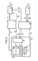
- the circuit which is shown in FIG. 3 as a block diagram, is implemented in each of the concentrators 2. It has a logic unit 8, consisting of a buffer memory 86, a change decoder 80, a transmission control unit 81, a status register 82 and an OR gate 83, a FIFO memory 7, a transmitter 10, a receiver 9 and a control unit 22.
- a logic unit 8 consisting of a buffer memory 86, a change decoder 80, a transmission control unit 81, a status register 82 and an OR gate 83, a FIFO memory 7, a transmitter 10, a receiver 9 and a control unit 22.
- the circuit is connected to the end points 30 via the wire pairs 6 to the outside. Furthermore, 3 HDLC messages are received via the reception lines 3 'of the signaling bus 3 and HDLC messages are sent to the central processing unit 1 via the transmission line 3' '.
- the operation of the individual end points 30 differs individually according to the time, frequency and duration. However, to ensure short response times, it must be ensured that every request for commissioning is carried out immediately or at least immediately acknowledged by a message signal.
- each terminal 30 in the logic unit 8 is therefore assigned a first buffer register 84 for the serial recording and intermediate storage of an incoming signaling information. All end points 30 are queried and the first buffer registers 84 written in each case after a predetermined time interval. Before that, however, their old contents are stored in second buffer registers 85 in order to be able to determine a change in the data stream if necessary by bitwise comparison.
- the second buffer register 85 consists of flip-flops with preparatory inputs (T-flip-flops) that are their Accept the input state to the output each time a polling cycle of the end stations 30 has ended.
- the input / output comparison is carried out via the change detectors 80.
- the outputs of these are routed to the status register 82, which is designed as a shift register, in such a way that a specific change detector 80 is assigned to each bit position.
- the associated status register position is thus made log. 1 set.
- a flag is then generated which indicates that a change has taken place on a specific data channel 6.
- Each change detector 80 consists of exclusive NOR gates 87, which are connected on the input side to respectively assigned register positions of the buffer registers 84 and 85, an XOR register 88 at the outputs of the exclusive NOR gates 87 and an OR gate 89 at the outputs of the XOR register 88. All the buffer registers 84, 85, all the XOR registers 88 and the status register 82 are connected via an internal data bus 11 to a buffer store in the form of a FIFO memory 7. This ensures that all relevant data relating to the change can be temporarily stored and transferred.
- All outputs of the status register 82 are connected to the OR gate 83, so a log at its output. 1 can be tapped if a signal change has taken place on one of the data channels 6.
- a log. 1 (flag set) indicates the status "data ready”. This is queried and evaluated cyclically in a first operating mode A in the configuration according to FIG. 3 by the central processing unit 1. In a second operating mode B, this state triggers the access of a local pre-computer 40, which pre-processes the signaling data (FIG. 7).
- the command is forwarded to the local control unit 22 via parallel lines 25.
- the command is interpreted by the control unit 22 and the signal "data ready” on line 15 is queried. If this is set, a command "start transmission” is given to the transmitter 10 via the line 17.
- a command is given to the transmission control unit 81 via line 13, which requests it to start the transmission of the relevant data via the internal data bus 11 and to make it available in the FIFO memory 7 for output on the transmission line 3 ′′.
- the memory content is read out by the transmitter 10 and output to the signal bus 3 in an information field of a so-called “I frame” (see FIG. 7).
- the transmission control unit 81 is shown via lines 12 whether the FIFI memory 7 is completely occupied.
- the transmitter 10 receives a message via line 16 when the FIFO memory 7 is not occupied. It thus serves as the end criterion for the transmitter 10.
- the information provided by the logic unit 8 can be called up as often as required by the central processing unit 1. Only after receipt of a receipt from the centr. Computing unit 1, which has a Line 26 is forwarded to the control unit 22, a delete signal is transmitted via line 14 to the transmission control unit 81.
- the status register 82 and the XOR register 88 are cleared and the first buffer registers 83 are released for the reception of new signaling data from the data channels 6.
- the format of an I-frame has several fields.
- the first field contains an opening byte consisting of a specified 0-1 combination.
- the second field contains the sender address.
- the following fields are intended to accommodate two control bytes with which a positive or negative redundancy check is possible.
- the end of the frame is formed by an end byte with a predetermined bit pattern.
- the RR frame according to FIG. 6 consists only of the opening field, address field, frame definition field, test fields and end field as defined in the HDLC protocol.
- Each concentrator 2 has a front-end computer 40, for example a microprocessor, for carrying it out.
- This is interrupt-controlled, i.e. as soon as a control signal is present at its interrupt input, it interrupts its current programs and starts a predetermined program.
- the following process steps are carried out:
- the signaling data coming from the logic unit 8 via the internal data bus 11 are subjected to preprocessing in the front-end computer 40 before they are written into the FIFO memory 7 via the internal BUS 11 '.
- all control signals "delete data” or “data ready” coming from the control unit 22 and the logic unit 8 are fed to the front-end computer 40 via a control register 23. This controls the control unit 22 and the logic unit 8 via a command output register 24.
- the signal "data ready" on line 15 indicates to the computer 40 an interruption request from the logic unit 8.
- the latter then reads the status register 82, the selected second buffer registers 85 and the XOR register 88. These registers are blocked in their state until the upstream computer via line 14 initiates deletion and release with a receipt.
- the upstream computer pre-processes the data (for example digit integration) and enters the data compressed in this way into the FIFO memory 7.
- the data is temporarily stored there until it is retrieved by a query from the master and has been positively acknowledged.
- the method means that the transmission path between the request and the response is not unnecessarily blocked by a reaction time.
- the data packet to be fetched was thus prepared while the master queried other slaves.
Landscapes
- Engineering & Computer Science (AREA)
- Computer Networks & Wireless Communication (AREA)
- Theoretical Computer Science (AREA)
- Signal Processing (AREA)
- Physics & Mathematics (AREA)
- General Engineering & Computer Science (AREA)
- General Physics & Mathematics (AREA)
- Small-Scale Networks (AREA)
- Data Exchanges In Wide-Area Networks (AREA)
- Communication Control (AREA)
Priority Applications (1)
| Application Number | Priority Date | Filing Date | Title |
|---|---|---|---|
| AT84109460T ATE42847T1 (de) | 1983-08-12 | 1984-08-08 | Datenuebertragungsverfahren in einem digitalen uebertragungsnetzwerk und vorrichtung zur durchfuehrung des verfahrens. |
Applications Claiming Priority (2)
| Application Number | Priority Date | Filing Date | Title |
|---|---|---|---|
| DE3329228 | 1983-08-12 | ||
| DE19833329228 DE3329228A1 (de) | 1983-08-12 | 1983-08-12 | Datenuebertragungsverfahren in einem digitalen uebertragungsnetzwerk und vorrichtung zur durchfuehrung des verfahrens |
Publications (2)
| Publication Number | Publication Date |
|---|---|
| EP0133577A1 true EP0133577A1 (fr) | 1985-02-27 |
| EP0133577B1 EP0133577B1 (fr) | 1989-05-03 |
Family
ID=6206447
Family Applications (1)
| Application Number | Title | Priority Date | Filing Date |
|---|---|---|---|
| EP84109460A Expired EP0133577B1 (fr) | 1983-08-12 | 1984-08-08 | Système de transmission de données dans un réseau de transmission numérique et dispositif pour l'application de ce système |
Country Status (5)
| Country | Link |
|---|---|
| US (1) | US4930103A (fr) |
| EP (1) | EP0133577B1 (fr) |
| JP (1) | JPS6054549A (fr) |
| AT (1) | ATE42847T1 (fr) |
| DE (2) | DE3329228A1 (fr) |
Cited By (3)
| Publication number | Priority date | Publication date | Assignee | Title |
|---|---|---|---|---|
| EP0218362A3 (en) * | 1985-09-20 | 1988-07-06 | Unisys Corporation | Distributed electronic mailbox system |
| EP0360022A1 (fr) * | 1988-09-09 | 1990-03-28 | Siemens Aktiengesellschaft | Circuit pour installations de télécommunication en particulier autocommutateurs dans lesquels des équipements individuels sont cycliquement commandés par un équipement commun |
| EP0425731A1 (fr) * | 1989-11-03 | 1991-05-08 | Siemens Aktiengesellschaft | Dispositif de commande d'un système à bus pour un multiplexeur programmable et flexible de signaux numériques |
Families Citing this family (4)
| Publication number | Priority date | Publication date | Assignee | Title |
|---|---|---|---|---|
| JP3977484B2 (ja) * | 1997-05-08 | 2007-09-19 | 矢崎総業株式会社 | 状態情報の管理方法及び通信システム |
| US20020152060A1 (en) * | 1998-08-31 | 2002-10-17 | Tseng Ping-Sheng | Inter-chip communication system |
| WO2006129579A1 (fr) * | 2005-05-31 | 2006-12-07 | Nec Corporation | Méthode et appareil pour transférer des signaux entre des dispositifs |
| US10474597B2 (en) * | 2015-08-03 | 2019-11-12 | Marvell World Trade Ltd. | Systems and methods for performing unknown address discovery in a MoChi space |
Citations (4)
| Publication number | Priority date | Publication date | Assignee | Title |
|---|---|---|---|---|
| DE2126456A1 (de) * | 1970-05-27 | 1971-12-09 | Plessey Handel Investment Ag | Datenübertragungsanordnung |
| DE2257164A1 (de) * | 1972-11-22 | 1974-05-30 | Tekade Felten & Guilleaume | Verfahren zur gesicherten datenuebertragung |
| US4001785A (en) * | 1974-02-15 | 1977-01-04 | Asahi Kasei Kogyo Kabushiki Kaisha | Apparatus for monitoring changes of multiple inputs |
| EP0037499A2 (fr) * | 1980-03-27 | 1981-10-14 | CSELT Centro Studi e Laboratori Telecomunicazioni S.p.A. | Dispositif faisant interface entre un bus d'un microprocesseur et un périphérie synchrone d'explorateurs et de distributeurs |
Family Cites Families (13)
| Publication number | Priority date | Publication date | Assignee | Title |
|---|---|---|---|---|
| JPS5246285A (en) * | 1975-10-08 | 1977-04-12 | Hitachi Ltd | Distant supervisory control |
| US4075691A (en) * | 1975-11-06 | 1978-02-21 | Bunker Ramo Corporation | Communication control unit |
| US4079452A (en) * | 1976-06-15 | 1978-03-14 | Bunker Ramo Corporation | Programmable controller with modular firmware for communication control |
| US4153945A (en) * | 1977-06-20 | 1979-05-08 | International Business Machines Corporation | Multiplexed control subsystem for sensor based systems |
| US4155071A (en) * | 1977-08-30 | 1979-05-15 | The Singer Company | Digital data change-of-state detector |
| US4219881A (en) * | 1977-12-30 | 1980-08-26 | Honeywell Inc. | Digital input control circuit |
| US4383295A (en) * | 1979-02-09 | 1983-05-10 | Honeywell Information Systems Inc. | Data processing system having data entry backspace character apparatus |
| JPS5953573B2 (ja) * | 1979-03-20 | 1984-12-26 | 富士通株式会社 | デ−タ伝送システム |
| JPS5634256A (en) * | 1979-08-29 | 1981-04-06 | Fuji Electric Co Ltd | Data transmission system |
| JPS5652949A (en) * | 1979-10-05 | 1981-05-12 | Hitachi Ltd | Interruption control method |
| US4426679A (en) * | 1980-09-29 | 1984-01-17 | Honeywell Information Systems Inc. | Communication multiplexer using a random access memory for storing an acknowledge response to an input/output command from a central processor |
| JPS57106258A (en) * | 1980-12-23 | 1982-07-02 | Hitachi Ltd | Transmission system for status change data |
| JPS5856553A (ja) * | 1981-09-30 | 1983-04-04 | Fujitsu Ltd | 状態変化検出回路 |
-
1983
- 1983-08-12 DE DE19833329228 patent/DE3329228A1/de not_active Withdrawn
-
1984
- 1984-08-08 DE DE8484109460T patent/DE3478062D1/de not_active Expired
- 1984-08-08 AT AT84109460T patent/ATE42847T1/de not_active IP Right Cessation
- 1984-08-08 EP EP84109460A patent/EP0133577B1/fr not_active Expired
- 1984-08-09 JP JP59167254A patent/JPS6054549A/ja active Pending
-
1986
- 1986-10-16 US US06/918,692 patent/US4930103A/en not_active Expired - Lifetime
Patent Citations (4)
| Publication number | Priority date | Publication date | Assignee | Title |
|---|---|---|---|---|
| DE2126456A1 (de) * | 1970-05-27 | 1971-12-09 | Plessey Handel Investment Ag | Datenübertragungsanordnung |
| DE2257164A1 (de) * | 1972-11-22 | 1974-05-30 | Tekade Felten & Guilleaume | Verfahren zur gesicherten datenuebertragung |
| US4001785A (en) * | 1974-02-15 | 1977-01-04 | Asahi Kasei Kogyo Kabushiki Kaisha | Apparatus for monitoring changes of multiple inputs |
| EP0037499A2 (fr) * | 1980-03-27 | 1981-10-14 | CSELT Centro Studi e Laboratori Telecomunicazioni S.p.A. | Dispositif faisant interface entre un bus d'un microprocesseur et un périphérie synchrone d'explorateurs et de distributeurs |
Non-Patent Citations (3)
| Title |
|---|
| PATENTS ABSTRACTS OF JAPAN, Band 1, Nr. 109, 24. September 1977, Seite 3213M77; & JP - A - 52 46285 (HITACHI SEISAKUSHO) 14.04.1977 * |
| PATENTS ABSTRACTS OF JAPAN, Band 7, Nr. 144(E-183)(1289), 23. Juni 1983; & JP - A - 58 56553 (FUJITSU K.K.) 04.04.1983 * |
| WESCON CONFERENCE RECORD, Band 24, 16.-18. September 1980, Seiten 1/2-1 bis 1/2-16, Anaheim, USA; R.L. EVANS: "Data communications for standalone minicomputers" * |
Cited By (4)
| Publication number | Priority date | Publication date | Assignee | Title |
|---|---|---|---|---|
| EP0218362A3 (en) * | 1985-09-20 | 1988-07-06 | Unisys Corporation | Distributed electronic mailbox system |
| EP0360022A1 (fr) * | 1988-09-09 | 1990-03-28 | Siemens Aktiengesellschaft | Circuit pour installations de télécommunication en particulier autocommutateurs dans lesquels des équipements individuels sont cycliquement commandés par un équipement commun |
| EP0425731A1 (fr) * | 1989-11-03 | 1991-05-08 | Siemens Aktiengesellschaft | Dispositif de commande d'un système à bus pour un multiplexeur programmable et flexible de signaux numériques |
| WO1991007031A1 (fr) * | 1989-11-03 | 1991-05-16 | Siemens Aktiengesellschaft | Bus controleur pour un multiplexeur de signaux numeriques souple et programmable |
Also Published As
| Publication number | Publication date |
|---|---|
| JPS6054549A (ja) | 1985-03-29 |
| US4930103A (en) | 1990-05-29 |
| DE3478062D1 (en) | 1989-06-08 |
| ATE42847T1 (de) | 1989-05-15 |
| DE3329228A1 (de) | 1985-02-21 |
| EP0133577B1 (fr) | 1989-05-03 |
Similar Documents
| Publication | Publication Date | Title |
|---|---|---|
| DE69028267T2 (de) | Paketvermittlungsnetzwerk mit Rundsendefähigkeit | |
| DE69213779T2 (de) | Verfahren und System für die Steuerung der Paketrate im Nachrichtennetz | |
| DE3041600C2 (de) | Verfahren und Schaltungsanordnung zum Übertragen von Datensignalen zwischen an Datenvermittlungseinrichtungen einer Datenvermittlungsanlage angeschlossenen Datensignalsendern und Datensignalempfängern | |
| DE3786298T2 (de) | Verfahren und Schalter zum Vermitteln von Informationen. | |
| DE69028266T2 (de) | Paketvermittlungsnetzwerk für unterschiedliche Typen von Paketen | |
| DE102013207826B3 (de) | Verfahren zum Betreiben eines Slave-Knotens eines digitalen Bussystems | |
| DE4232667A1 (de) | Rechnergesteuerte vermittlungsanlage | |
| DE3586919T2 (de) | Verfahren zur steuerung von informationsuebertragung. | |
| DE69024641T2 (de) | Schnittstelle für Zugang als Sender und Empfänger gestützt auf synchroner Übertragung in einem verteilten Netz | |
| EP0184706B1 (fr) | Montage d'interface | |
| DE3041556C2 (de) | Verfahren und Schaltungsanordnung zur Vermittlung von Daten zwischen Datenendgeräten | |
| DE69127971T2 (de) | Verfahren und vorrichtung zur ziel- und quellenadressierung in einem paketnetz | |
| EP0133577B1 (fr) | Système de transmission de données dans un réseau de transmission numérique et dispositif pour l'application de ce système | |
| DE69326378T2 (de) | Steuerung des Austauschens von Datenpaketen in einem Netzwerk | |
| CH656276A5 (de) | Verfahren und schaltungsanordnung zum uebertragen von datensignalen zwischen datenvermittlungseinrichtungen einer datenvermittlungsanlage. | |
| EP0447769A2 (fr) | Méthode et dispositif de gestion d'unité uniformes et élément de commutation | |
| EP0105212B1 (fr) | Montage de circuit pour la transmission de signaux entre une ligne d'abonné et au moins une ligne de transmission d'un centre de télécommunications à services integrés | |
| DE19911830A1 (de) | Verfahren zum Verwalten des Zugriffs auf einen Bus und Bussystem | |
| DE3324504C1 (de) | Verfahren zur Informationsuebertragung zwischen Mikrorechnern in einem dezentralen Prozesssteuersystem,insbesondere fuer Fernsprechanlagen | |
| CH656274A5 (de) | Schaltungsanordnung zum uebertragen von datensignalen zwischen jeweils zwei datenendgeraeten einer datenuebertragungsanlage. | |
| DE69021626T2 (de) | Eingebettete Steuertechnik für verteilte Steuersysteme. | |
| DE4243266C2 (de) | Verfahren zum Betrieb einer Kommunikationsschaltvorrichtung | |
| DE69110192T2 (de) | Vermittlungsmodul digitaler Datenpakete zur Zuweisung leerer Pakete an einen Koppelpunkt. | |
| EP0475180A1 (fr) | Procédé de transmission de paquets de communication entre des lignes de raccordement existantes dans un commutateur | |
| DE19808680A1 (de) | Verfahren und Vorrichtung zur Bearbeitung von über einen Datenkanal empfangenen oder zu übertragenden Datenpaketen |
Legal Events
| Date | Code | Title | Description |
|---|---|---|---|
| PUAI | Public reference made under article 153(3) epc to a published international application that has entered the european phase |
Free format text: ORIGINAL CODE: 0009012 |
|
| AK | Designated contracting states |
Designated state(s): AT CH DE FR GB IT LI NL SE |
|
| 17P | Request for examination filed |
Effective date: 19850627 |
|
| 17Q | First examination report despatched |
Effective date: 19860730 |
|
| GRAA | (expected) grant |
Free format text: ORIGINAL CODE: 0009210 |
|
| AK | Designated contracting states |
Kind code of ref document: B1 Designated state(s): AT CH DE FR GB IT LI NL SE |
|
| REF | Corresponds to: |
Ref document number: 42847 Country of ref document: AT Date of ref document: 19890515 Kind code of ref document: T |
|
| REF | Corresponds to: |
Ref document number: 3478062 Country of ref document: DE Date of ref document: 19890608 |
|
| ET | Fr: translation filed | ||
| ITF | It: translation for a ep patent filed | ||
| GBT | Gb: translation of ep patent filed (gb section 77(6)(a)/1977) | ||
| PLBI | Opposition filed |
Free format text: ORIGINAL CODE: 0009260 |
|
| 26 | Opposition filed |
Opponent name: AEG AKTIENGESELLSCHAFT Effective date: 19900130 |
|
| NLR1 | Nl: opposition has been filed with the epo |
Opponent name: AEG AG |
|
| PGFP | Annual fee paid to national office [announced via postgrant information from national office to epo] |
Ref country code: DE Payment date: 19901025 Year of fee payment: 7 |
|
| PGFP | Annual fee paid to national office [announced via postgrant information from national office to epo] |
Ref country code: CH Payment date: 19901123 Year of fee payment: 7 |
|
| PGFP | Annual fee paid to national office [announced via postgrant information from national office to epo] |
Ref country code: GB Payment date: 19910718 Year of fee payment: 8 |
|
| PGFP | Annual fee paid to national office [announced via postgrant information from national office to epo] |
Ref country code: AT Payment date: 19910726 Year of fee payment: 8 |
|
| PGFP | Annual fee paid to national office [announced via postgrant information from national office to epo] |
Ref country code: SE Payment date: 19910816 Year of fee payment: 8 |
|
| PGFP | Annual fee paid to national office [announced via postgrant information from national office to epo] |
Ref country code: FR Payment date: 19910823 Year of fee payment: 8 |
|
| ITTA | It: last paid annual fee | ||
| PGFP | Annual fee paid to national office [announced via postgrant information from national office to epo] |
Ref country code: NL Payment date: 19910831 Year of fee payment: 8 |
|
| RDAG | Patent revoked |
Free format text: ORIGINAL CODE: 0009271 |
|
| STAA | Information on the status of an ep patent application or granted ep patent |
Free format text: STATUS: PATENT REVOKED |
|
| REG | Reference to a national code |
Ref country code: CH Ref legal event code: PL |
|
| 27W | Patent revoked |
Effective date: 19910727 |
|
| GBPR | Gb: patent revoked under art. 102 of the ep convention designating the uk as contracting state | ||
| NLR2 | Nl: decision of opposition | ||
| EUG | Se: european patent has lapsed |
Ref document number: 84109460.0 Effective date: 19911218 |