EP0134402A1 - Integrierte Injektionslogikschaltung - Google Patents
Integrierte Injektionslogikschaltung Download PDFInfo
- Publication number
- EP0134402A1 EP0134402A1 EP84105151A EP84105151A EP0134402A1 EP 0134402 A1 EP0134402 A1 EP 0134402A1 EP 84105151 A EP84105151 A EP 84105151A EP 84105151 A EP84105151 A EP 84105151A EP 0134402 A1 EP0134402 A1 EP 0134402A1
- Authority
- EP
- European Patent Office
- Prior art keywords
- constant current
- circuits
- reference potential
- current source
- circuit
- Prior art date
- Legal status (The legal status is an assumption and is not a legal conclusion. Google has not performed a legal analysis and makes no representation as to the accuracy of the status listed.)
- Granted
Links
Images


Classifications
-
- H—ELECTRICITY
- H03—ELECTRONIC CIRCUITRY
- H03K—PULSE TECHNIQUE
- H03K19/00—Logic circuits, i.e. having at least two inputs acting on one output; Inverting circuits
- H03K19/02—Logic circuits, i.e. having at least two inputs acting on one output; Inverting circuits using specified components
- H03K19/08—Logic circuits, i.e. having at least two inputs acting on one output; Inverting circuits using specified components using semiconductor devices
- H03K19/082—Logic circuits, i.e. having at least two inputs acting on one output; Inverting circuits using specified components using semiconductor devices using bipolar transistors
- H03K19/091—Integrated injection logic or merged transistor logic
-
- H—ELECTRICITY
- H03—ELECTRONIC CIRCUITRY
- H03M—CODING; DECODING; CODE CONVERSION IN GENERAL
- H03M1/00—Analogue/digital conversion; Digital/analogue conversion
- H03M1/66—Digital/analogue converters
- H03M1/74—Simultaneous conversion
- H03M1/742—Simultaneous conversion using current sources as quantisation value generators
- H03M1/745—Simultaneous conversion using current sources as quantisation value generators with weighted currents
Definitions
- the present invention relates to improvements of an integrated injection logic circuit.
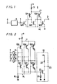
- I 2 L circuit A conventional integrated injection logic circuit (hereinafter simply referred to as I 2 L circuit ) will hereinafter be described with reference to Fig. 1.
- reference numeral 6 generally designates an I 2 L circuit wherein reference numerals 1 and 2 respectively designate input and output terminals thereof.
- Reference characters Qll and Q12 respectively designate constant current source transistors of PN P type and Q21 and Q22 switching inverter transistors of NPN type...:The emitters of the transistors Qll and Q12 are connected together to an injector IJ and the injector IJ is connected through a resistor 3 to a voltage source +B (for example, +5V).
- +B for example, +5V
- the collectors of the transistors Qll and Q12 are respectively connected to the bases of the transistors Q21 and Q22, and the collector of the transistor Q21 is connected to the base of the transistor Q22.
- the emitters of the transistors Q21 and Q22 and the bases of the transistors Qll and Q12 are all connected to a wall WL and the wall WL is grounded.
- a unit circuit formed of a constant current source transistor and a switching inverter transistor supplied at its base with the constant current from the constant current source transistor can arbitrarily be connected in cascade between the injector IJ and the wall WL.
- an NPN transistor Q20 is provided the collector of which is connected to the base of the transistor Q21.
- the emitter thereof is connectec to the wall WL and from the base of which is led out the input terminal 1.
- the output terminal 2 is led out from the collector of the transistor Q22.
- Reference numeral 4 designates an output terminal of a circuit to be connected to the I 2 L curcuit 6 at its input side. This output terminal 4 is connected through an interface circuit 5 to the input terminal 1 of the I 2 L circuit 6.
- the logic high level and the logic low level developed at the output terminal 2 of such I 2 L circuit 6 are respectively about 0.7V and OV. Accordingly, when the logic high level and the logic low level of the output developed at the output terminal 4 of the circuit (for example, TTL (transistor-transistor logic) circuit) to be connected to the input side of the I 2 L circuit 6 are respectively 4V and 1V, since the withstanding voltage of the I 2 L circuit 6 is approximately 1.4V, the input interface circuit 5 connected therebetween must have a quite complicated structure.
- TTL transistor-transistor logic
- FIG. 2 An example of the 3-bit D/A (digital-to-analog) converter using such I 2 L circuit as a gate circuit will be described with reference to Fig. 2.
- Reference numerals 11, 12 and 13 respectively designate input terminals of 3-bit digital signals, and the 3-bit digital signals are respectively supplied therefrom to gate circuits 14, 15 and 16, each of which is formed of the I 2 L circuit.
- Reference numerals Q31,- Q32 and Q33 respectively designate first constant current source transistors of PNP type and the transistors Q32 and Q33 are made as multi-transistors. The ratio of the collector currents of the transistors Q31, Q32 and Q33 is selected as 1:2:4.
- the emitters of the transistors Q31, Q32 and Q33 are respectively connected through an injector IJ and a resistor 17 to the voltage source +B.
- Reference numerals Q41, Q42 and Q 4 3 respectively designate second constant current source transistors of PNP type, and the transistors Q42 and Q43 are made as multi-transistors.
- the ratio of the collector currents of the transistors Q41, Q42 and Q43 is selected also as 1:2:4, and the emitters of the transistors Q41, Q42 and Q43 are respectively connected to the collectors of the transistors Q31, Q32 and Q33 and the collectors of the transistors Q41, Q42 and Q43 are connected together.
- the bases of the transistors Q31 to Q33 and Q41 to Q43 are respectively connected to the wall WL and the wall WL is grounded through a diode 18.
- Reference numeral 19 designates a current to voltage converting circuit.
- the collectors of the transistors Q41 to Q43 are connected together to a base of an NPN transistor 20 in the circuit 19 and the base of the transistor 20 is grounded through a diode 21.
- the emitter of the transistor 20 is grounded and the collector thereof is connected through a load resistor 22 to the voltage source +B and connected to an output terminal 23.
- This D/A converter requires the current to voltage converting circuit 19 because the above I 2 L circuit shown in Fig. 1 is used as the gate circuits 14 to 16 thereof. As a result, the non-linear factor such as Early effect or the like of the output transistor 20 is added to the output of the D/A converter, thus obstructing the characteristic of the D/A converter from being improved.
- an object of the present invention is to provide an improved I 2 L (integrated injection logic) circuit.
- Another object ot the present invention is to provide an I 2 L circuit which can simplify the circuit arrangement of an input interface circuit.
- a further object of the present invention is to provide a D/A (digital-to-analog) converter having excellent precision as compared with a conventional D/A converter.
- an integrated injection logic circuit comprising:
- I 2 L integrated injection logic
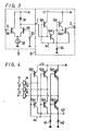
- the injector IJ to which the emitters of the constant current source transistors Qll and Q12 of NPN type are all connected is directly coupled to the voltage source +B (for example, +5V).
- the emitters of the switching inverter transistors Q21 and Q22 of NPN type and the bases of the constant current source transistors Qll and Q12 are respectively connected to the wall WL, and the wall WL is grounded through a bias resistor 34.
- the bias resistor 34 may be replaced with a constant current source.
- Reference numeral 4 designates the output terminal of the circuit (for example, TTL circuit) to be connected to the I 2 L circuit 6 at its input side.
- This output terminal 4 is connected to the base of a first transistor Ql of NPN transistors Ql and Q2 of a differential transistor configuration.
- the emitters.of the transistors Q1 and Q2 are together grounded through a constant current source 32, and the base of the transistor Q2 is connected to a reference potential source 33.
- the collector of the transistor Ql is directly connected to the voltage source B, while the collector of the transistor Q2 is connected through a resistor 31 to the voltage source +B and directly to the input terminal 1 which is led out from the base of the transistor Q21 in the 1 2L circuit 6.
- the voltage of the reference potential source 33 is selected to be, for example, 2.5V.
- the logic high level of the output developed at the output terminal 2 is 5V and the logic.low level thereof is 4.3V, respectively. Consequently, if the circuit such as the TTL circuit having the logic high level of 4V and the logic low level of 1V is connected to the input side of the I 2 L circuit 6, the input interface circuit 5 can be constructed by the circuit with the simple circuit arrangement as shown in Fig. 3.
- FIG. 4 An example of a D/A converter using the I 2 L circuit of the present invention shown in Fig. 3 as its gate circuits will be described with reference to Fig. 4.
- the I 2 L circuit of the present invention described in connection with Fig. 3 is used as each of the gate circuits 14, 15 and 16.
- the injector IJ to which the emitters of the first constant current source transistors Q31, Q32 and Q33 are connected is directly connected to the voltage source + B .
- the collectors of the second constant current source transistors Q41, Q42 and Q43 are connected together from which an output terminal 43 is led out and which is grounded through a load resistor 42. Further, the wall WL to which the bases of the transistors Q31 to Q33 and Q41 to Q43 are connected is grounded through a bias resistor 41.
- the D/A converter shown in Fig. 4 does not require the current to voltage converting circuit so that the non-linear factor such as Early effect or the like of the output transistor is never added to the output of the D/A converter, thus the D/A converter with excellent characteristic being obtained.
- Reference numerals 14 to 16 designate the gate circuits for the input terminals 11 to 13, each gate circuit being formed of the I 2 L circuit as set forth above. More particularly, each of the gate circuits 14 to 16 is formed of the constant current source transistor Qll of PNP type and the switching inverter transistor Q21 of NPN type. Reference numerals Kl to K3 respectively designate constant current circuits, each of which is formed of a series circuit of the PNP transistors Q31 to Q33 and Q41 to Q43.
- the emitters of the NPN transistors Q21 in the gate circuit 14 to 16 and the bases of the PNP transistors Q31 to Q33 and Q41 to Q43 are all connected to the common wall WL. Then, an analog signal based on the sum of constant currents from the constant current circuits which are selected in response to the digital signals supplied to the input terminals 11 to 13 is developed at the output terminal 43.
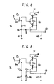
- Fig. 6 shows the gate circuit 14 of Fig. 5 (where one transistor Qll is omitted) and the constant current circuit Kl thereof in an extracted fashion. Accordingly, in Fig. 6, like parts corresponding to those in Fig. 5 are marked with the same references.
- reference numeral 9 designates a wall resistor (distributed resistor) and 8 a distributed resistor between the emitter of the transistor Q21 and the wall WL.
- a reedback circuit is used in place of the bias resistor 41 to make the potential at the wall WL constant.
- the resistor component 9 exists in the wall WL, the potential at the wall WL becomes constant.
- the potential at the wall WL is changed by the currents flowing from the respective constant current circuits to the wall WL, thus the above problem being left unsolved.
- Fig. 7 Another embodiment of the D/A converter according to the present invention will hereinafter be described with reference to Fig. 7.
- the injector IJ is common to the gate circuits 14 to 16 and the constant current circuits Kl to K3, but a wall WL a of the gate circuits 14 to 16 is separate from a wall WL b of the constant current circuits Kl to K3, and these walls WL a and WL b are respectively grounded through separate bias resistors 41a and 41b.
- These bias resistors 41a and 41b may be replaced with constant current sources, respectively.
- the other circuit arrangement of Fig. 7 is the same as that in Fi g . 5.
- Fig. 8 shows the gate circuit 14 (the transistor Qll is omitted) and the constant current circuit Kl in Fig. 7 in an extracted manner.
- the collector of the transistor Q21 is at high level, the current I 0 injected from the injector IJ is flowed into the load resistor 42 so that the analog voltage is developed at the output terminal 43.
- the sum current of the base currents of the transistors Q31 and Q41 is flowed in the wall WL b of the constant current circuit Kl.
- the current 1 0 injected from the injector IJ is flowed through the transistor Q21 to the wall ML a of the gate circuit 14 so that only the base current of the transistor Q31 is flowed into the wall WL b of the constant current circuit Kl.
- the current flowed into the wall WL b of the constant current circuit Kl becomes equal to the sum of the base currents of the transistors Q31 and Q41 in a certain case, while in other case, it becomes equal to the base current of the transistor Q31.
- the difference therebetween becomes equal to the value of the base current of the transistor Q41. Therefore, as compared with the D/A converter in Fig. 5, the change of the analog output voltage due to the fluctuation of the current flowed into the wall becomes considerably small so that the precision of the D/A converter becomes significantly high.
Landscapes
- Engineering & Computer Science (AREA)
- Theoretical Computer Science (AREA)
- Power Engineering (AREA)
- Physics & Mathematics (AREA)
- Computer Hardware Design (AREA)
- Computing Systems (AREA)
- General Engineering & Computer Science (AREA)
- Mathematical Physics (AREA)
- Logic Circuits (AREA)
- Analogue/Digital Conversion (AREA)
Priority Applications (1)
| Application Number | Priority Date | Filing Date | Title |
|---|---|---|---|
| AT84105151T ATE36102T1 (de) | 1983-05-09 | 1984-05-07 | Integrierte injektionslogikschaltung. |
Applications Claiming Priority (4)
| Application Number | Priority Date | Filing Date | Title |
|---|---|---|---|
| JP68940/83U | 1983-05-09 | ||
| JP8062183A JPS59205826A (ja) | 1983-05-09 | 1983-05-09 | I↑2l回路 |
| JP6894083U JPS59174735U (ja) | 1983-05-09 | 1983-05-09 | D/aコンバ−タ |
| JP80621/83 | 1983-05-09 |
Publications (2)
| Publication Number | Publication Date |
|---|---|
| EP0134402A1 true EP0134402A1 (de) | 1985-03-20 |
| EP0134402B1 EP0134402B1 (de) | 1988-07-27 |
Family
ID=26410127
Family Applications (1)
| Application Number | Title | Priority Date | Filing Date |
|---|---|---|---|
| EP84105151A Expired EP0134402B1 (de) | 1983-05-09 | 1984-05-07 | Integrierte Injektionslogikschaltung |
Country Status (6)
| Country | Link |
|---|---|
| US (1) | US4602244A (de) |
| EP (1) | EP0134402B1 (de) |
| AT (1) | ATE36102T1 (de) |
| AU (1) | AU570246B2 (de) |
| CA (1) | CA1287406C (de) |
| DE (1) | DE3473104D1 (de) |
Families Citing this family (2)
| Publication number | Priority date | Publication date | Assignee | Title |
|---|---|---|---|---|
| US4602244A (en) * | 1983-05-09 | 1986-07-22 | Sony Corporation | Integrated injection logic circuit |
| US5508702A (en) * | 1994-06-17 | 1996-04-16 | National Semiconductor Corp. | BiCOMS digital-to-analog conversion |
Citations (1)
| Publication number | Priority date | Publication date | Assignee | Title |
|---|---|---|---|---|
| EP0039945A2 (de) * | 1980-05-14 | 1981-11-18 | Kabushiki Kaisha Toshiba | I2L-Logikschaltung |
Family Cites Families (2)
| Publication number | Priority date | Publication date | Assignee | Title |
|---|---|---|---|---|
| US4602244A (en) * | 1983-05-09 | 1986-07-22 | Sony Corporation | Integrated injection logic circuit |
| US6693558B2 (en) * | 2001-06-18 | 2004-02-17 | Innovative Solutions & Support, Inc. | Aircraft flat panel display system |
-
1984
- 1984-04-27 US US06/604,486 patent/US4602244A/en not_active Expired - Lifetime
- 1984-05-07 EP EP84105151A patent/EP0134402B1/de not_active Expired
- 1984-05-07 DE DE8484105151T patent/DE3473104D1/de not_active Expired
- 1984-05-07 AT AT84105151T patent/ATE36102T1/de not_active IP Right Cessation
- 1984-05-08 CA CA000453767A patent/CA1287406C/en not_active Expired - Lifetime
- 1984-05-09 AU AU27839/84A patent/AU570246B2/en not_active Expired
Patent Citations (1)
| Publication number | Priority date | Publication date | Assignee | Title |
|---|---|---|---|---|
| EP0039945A2 (de) * | 1980-05-14 | 1981-11-18 | Kabushiki Kaisha Toshiba | I2L-Logikschaltung |
Non-Patent Citations (2)
| Title |
|---|
| ELECTRONICS, 3 October 1974; C.M. HART et al "Bipolar LSI takes a new direction with integrated injection logic", pages 111-118 * |
| IBM TECHNICAL DISCLOSURE BULLETIN vol. 24, no. 6, November 1981; H.H. BERGER "Injection current switch logic", pages 3089-3090 * |
Also Published As
| Publication number | Publication date |
|---|---|
| ATE36102T1 (de) | 1988-08-15 |
| EP0134402B1 (de) | 1988-07-27 |
| DE3473104D1 (en) | 1988-09-01 |
| AU570246B2 (en) | 1988-03-10 |
| CA1287406C (en) | 1991-08-06 |
| DE3473104T (de) | 1988-09-01 |
| US4602244A (en) | 1986-07-22 |
| AU2783984A (en) | 1984-11-15 |
Similar Documents
| Publication | Publication Date | Title |
|---|---|---|
| US4982119A (en) | Comparator with latch circuit | |
| EP0084722A1 (de) | Differenzverstärkerschaltungsanordnung | |
| US4760286A (en) | Comparator with input offset current elimination | |
| US4835771A (en) | Integrated digital multiplexer circuit | |
| US4435654A (en) | Output level adjustment means for low fanout ECL lacking emitter follower output | |
| KR950002090B1 (ko) | 논리 레벨 변환기 회로 | |
| EP0432577A1 (de) | ECL-Schaltung | |
| US5164658A (en) | Current transfer circuit | |
| US4754166A (en) | Reset circuit for integrated injection logic | |
| US5170079A (en) | Collector dot and circuit with latched comparator | |
| US4355246A (en) | Transistor-transistor logic circuit | |
| US4602244A (en) | Integrated injection logic circuit | |
| US4250407A (en) | Multi function patch pin circuit | |
| US4446385A (en) | Voltage comparator with a wide common mode input voltage range | |
| EP0098155B1 (de) | Schmitt-Trigger-Schaltung | |
| US3509364A (en) | Video amplifier particularly adapted for integrated circuit fabrication | |
| US4910425A (en) | Input buffer circuit | |
| EP0456127A1 (de) | Verstärker | |
| EP0076099B1 (de) | TTL-Schaltung | |
| US4536663A (en) | Comparator circuit having full supply common mode input | |
| US4156154A (en) | Flip-flop circuit | |
| US4485318A (en) | Interface circuit for an integrated injection logic circuit | |
| JPS6094531A (ja) | レベルアダプタ回路 | |
| EP0226351A2 (de) | Dreispannungspegeldetektor | |
| KR860000799B1 (ko) | 스위치 회로 |
Legal Events
| Date | Code | Title | Description |
|---|---|---|---|
| PUAI | Public reference made under article 153(3) epc to a published international application that has entered the european phase |
Free format text: ORIGINAL CODE: 0009012 |
|
| 17P | Request for examination filed |
Effective date: 19841108 |
|
| AK | Designated contracting states |
Designated state(s): AT DE FR GB NL |
|
| 17Q | First examination report despatched |
Effective date: 19860516 |
|
| R17C | First examination report despatched (corrected) |
Effective date: 19870129 |
|
| GRAA | (expected) grant |
Free format text: ORIGINAL CODE: 0009210 |
|
| AK | Designated contracting states |
Kind code of ref document: B1 Designated state(s): AT DE FR GB NL |
|
| REF | Corresponds to: |
Ref document number: 36102 Country of ref document: AT Date of ref document: 19880815 Kind code of ref document: T |
|
| REF | Corresponds to: |
Ref document number: 3473104 Country of ref document: DE Date of ref document: 19880901 |
|
| ET | Fr: translation filed | ||
| PLBE | No opposition filed within time limit |
Free format text: ORIGINAL CODE: 0009261 |
|
| STAA | Information on the status of an ep patent application or granted ep patent |
Free format text: STATUS: NO OPPOSITION FILED WITHIN TIME LIMIT |
|
| 26N | No opposition filed | ||
| REG | Reference to a national code |
Ref country code: GB Ref legal event code: IF02 |
|
| PGFP | Annual fee paid to national office [announced via postgrant information from national office to epo] |
Ref country code: GB Payment date: 20030507 Year of fee payment: 20 |
|
| PGFP | Annual fee paid to national office [announced via postgrant information from national office to epo] |
Ref country code: FR Payment date: 20030508 Year of fee payment: 20 |
|
| PGFP | Annual fee paid to national office [announced via postgrant information from national office to epo] |
Ref country code: AT Payment date: 20030514 Year of fee payment: 20 |
|
| PGFP | Annual fee paid to national office [announced via postgrant information from national office to epo] |
Ref country code: DE Payment date: 20030515 Year of fee payment: 20 |
|
| PGFP | Annual fee paid to national office [announced via postgrant information from national office to epo] |
Ref country code: NL Payment date: 20030530 Year of fee payment: 20 |
|
| PG25 | Lapsed in a contracting state [announced via postgrant information from national office to epo] |
Ref country code: GB Free format text: LAPSE BECAUSE OF EXPIRATION OF PROTECTION Effective date: 20040506 |
|
| PG25 | Lapsed in a contracting state [announced via postgrant information from national office to epo] |
Ref country code: NL Free format text: LAPSE BECAUSE OF EXPIRATION OF PROTECTION Effective date: 20040507 Ref country code: AT Free format text: LAPSE BECAUSE OF EXPIRATION OF PROTECTION Effective date: 20040507 |
|
| REG | Reference to a national code |
Ref country code: GB Ref legal event code: PE20 |
|
| NLV7 | Nl: ceased due to reaching the maximum lifetime of a patent |
Effective date: 20040507 |