EP0134453A2 - Procédé pour calculer la quantité de lumière pour les dispositifs lithographiques de copiage à projection - Google Patents
Procédé pour calculer la quantité de lumière pour les dispositifs lithographiques de copiage à projection Download PDFInfo
- Publication number
- EP0134453A2 EP0134453A2 EP84107434A EP84107434A EP0134453A2 EP 0134453 A2 EP0134453 A2 EP 0134453A2 EP 84107434 A EP84107434 A EP 84107434A EP 84107434 A EP84107434 A EP 84107434A EP 0134453 A2 EP0134453 A2 EP 0134453A2
- Authority
- EP
- European Patent Office
- Prior art keywords
- exposure
- wafers
- determining
- photoresist
- dose
- Prior art date
- Legal status (The legal status is an assumption and is not a legal conclusion. Google has not performed a legal analysis and makes no representation as to the accuracy of the status listed.)
- Granted
Links
Images
Classifications
-
- G—PHYSICS
- G03—PHOTOGRAPHY; CINEMATOGRAPHY; ANALOGOUS TECHNIQUES USING WAVES OTHER THAN OPTICAL WAVES; ELECTROGRAPHY; HOLOGRAPHY
- G03F—PHOTOMECHANICAL PRODUCTION OF TEXTURED OR PATTERNED SURFACES, e.g. FOR PRINTING, FOR PROCESSING OF SEMICONDUCTOR DEVICES; MATERIALS THEREFOR; ORIGINALS THEREFOR; APPARATUS SPECIALLY ADAPTED THEREFOR
- G03F7/00—Photomechanical, e.g. photolithographic, production of textured or patterned surfaces, e.g. printing surfaces; Materials therefor, e.g. comprising photoresists; Apparatus specially adapted therefor
- G03F7/70—Microphotolithographic exposure; Apparatus therefor
- G03F7/70483—Information management; Active and passive control; Testing; Wafer monitoring, e.g. pattern monitoring
- G03F7/7055—Exposure light control in all parts of the microlithographic apparatus, e.g. pulse length control or light interruption
- G03F7/70558—Dose control, i.e. achievement of a desired dose
-
- G—PHYSICS
- G03—PHOTOGRAPHY; CINEMATOGRAPHY; ANALOGOUS TECHNIQUES USING WAVES OTHER THAN OPTICAL WAVES; ELECTROGRAPHY; HOLOGRAPHY
- G03F—PHOTOMECHANICAL PRODUCTION OF TEXTURED OR PATTERNED SURFACES, e.g. FOR PRINTING, FOR PROCESSING OF SEMICONDUCTOR DEVICES; MATERIALS THEREFOR; ORIGINALS THEREFOR; APPARATUS SPECIALLY ADAPTED THEREFOR
- G03F7/00—Photomechanical, e.g. photolithographic, production of textured or patterned surfaces, e.g. printing surfaces; Materials therefor, e.g. comprising photoresists; Apparatus specially adapted therefor
- G03F7/004—Photosensitive materials
- G03F7/09—Photosensitive materials characterised by structural details, e.g. supports, auxiliary layers
- G03F7/105—Photosensitive materials characterised by structural details, e.g. supports, auxiliary layers having substances, e.g. indicators, for forming visible images
-
- G—PHYSICS
- G03—PHOTOGRAPHY; CINEMATOGRAPHY; ANALOGOUS TECHNIQUES USING WAVES OTHER THAN OPTICAL WAVES; ELECTROGRAPHY; HOLOGRAPHY
- G03F—PHOTOMECHANICAL PRODUCTION OF TEXTURED OR PATTERNED SURFACES, e.g. FOR PRINTING, FOR PROCESSING OF SEMICONDUCTOR DEVICES; MATERIALS THEREFOR; ORIGINALS THEREFOR; APPARATUS SPECIALLY ADAPTED THEREFOR
- G03F7/00—Photomechanical, e.g. photolithographic, production of textured or patterned surfaces, e.g. printing surfaces; Materials therefor, e.g. comprising photoresists; Apparatus specially adapted therefor
- G03F7/20—Exposure; Apparatus therefor
Definitions
- the present invention relates to a method for quantitatively determining the exposure dose associated with any exposure speed of a patterning exposure tool.
- Photolithographic instruments are used in the manufacture of integrated circuits.
- wafers of silicon are coated with a photoresist material.
- the photoresist material When exposed to ultraviolet light the photoresist material is polymerized into a hard tenacious coating and the unexposed portions of the layer may easily be removed by means of a solvent or developer.
- a mask or master which is opaque except for a pattern of transparent lines, the photoresist coating may be exposed to light in a pattern conforming to a circuit element or elements.
- a wafer may be exposed to successive masks, each of which exposes a new photoresist coating in a different pattern on its surface, forming additional circuit elements.
- the optical images formed on the wafer in successive exposures must, however, be closely controlled in relative position, for example, by use of patterning exposure tools, such as projection printers, lx scanning tools, reduction scanning tools, stepping and contact instruments, broadly defined as photolithography instruments.
- Typical photolithography projection printers used in exposing photoresist in such a manner are described in U.S. Patents 4,011,011, 4,068,947, 3,951,546, 3,937,556, 3,952,217, 4,248,508, 3,957,364, and 4.20.702, These printers operate without projection lenses made up of refractive elements, instead exposing the wafer through a mask by scanning the mask with an illumination source, preferably, a UV (Ultra Violet) source. Control of exposure times in patterning exposure tools is obtained by control of the speed of the scanning motion and of the width of the area illuminated on the mask, or by varying shutter speeds.
- an illumination source preferably, a UV (Ultra Violet) source.
- Another known method of dosimetry involves exposing a test photoresist layer through a mask which provides images of varying percent transmittance. After development, the photolithographic instrument dose is approximated for a known process window via SEM (Scanning Electron Micrograph) image analysis. This method, however, is not quantitative and is dependent on the type of photoresist, developer and processing. It also requires a scanning electron microscope.
- the known end point detection method of dosimetry involves the exposure of a test photoresist layer through a blank quartz mask after which a laser endpoint detection is run to determine dissolution curves.
- the photolithographic tool dose is approximated for a known process window via the laser endpoint detection dissolution data base.
- This method has the disadvantages that a laser endpoint detection system is required, it is not quantitative and is dependent on the type of photoresist, developer and laser endpoint detection procedure.
- Photoresist image analysis is also known as a method of dosimetry. After exposure and development, the relative dose is estimated as a function of line width from optical or electron microscopy techniques. A photolithographic tool dose can be approximated from an SEM image data base. Disadvantages of this method are that it requires a SEM or other microscope, is not quantitative, and is dependent on the type of photoresist, developer and processing.
- the object of the invention is to provide a method for determining the mid-, near- or deep UV exposure dose of a patterning exposure instrument as a function of scan speed or shutter speed which has low measurement error and which offers a measurement directly correlated with photoresist lithography usage by matching the photolithographic instrument performance with each lot or loading of photoresist.
- This method of dosimetry uses photoresist coated discs which do not require the use of adhesion promoters or prebake.
- the object of the invention is achieved by a method according to claim 1.
- the present invention overcomes the difficulties of determining exposure for photolithographic projection instruments without built-in photoelectric probes. More specifically, the above object has been attained by a method for determining the dose per exposure time of a photolithographic instrument by measuring the UV absorbance of a test photoresist layer deposited on a quartz disc. The dose is determined by comparing the bleaching value on a particular day for a particular tool to that of a calibration curve of bleaching versus dose. By the present method, photoresist response is specifically matched to the effective total dose for that resist, over the entire effective range of wavelengths in the exposure tool used.
- the optimal exposure speed on a given instrument to achieve the desired relative percent PAC bleached value for a given resist may be determined by simple direct reference to the curve generated for that photolithography production instrument.
- Exposure speed refers to the method for controlling exposure on a given patterning exposure tool, e.g., by varying scanning speed or shutter speed.
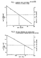
- Relative percent PAC bleached is determined as above by UV spectrophotometry, and a linear curve of relative percent PAC bleached is plotted against exposure speed. An example of such a curve is shown in Fig. 2.
- the actual dose (in mJ/cm 2 ) is determined quantitatively in terms of exposure speed on a given photolithography instrument by establishing from the two curves the dose and exposure speed necessary to obtain the same relative percent PAC bleached in the resist. This absolute determination is useful for comparison of different resists or processes, and provides, for example, a convenient and reliable quality check method for a given lot of resist.
- Absolute quantitative measurement of the dosage associated with any given scan or shutter speed is useful in many ways.
- a photolithographic tool for which a calibration curve is generated may be used to expose resists of different chemical composition, concentration or thickness at any known optimum dosage without the necessity of exposing new test wafers.
- UV absorbance spectra of each disc half were measured at 405 nm on a UV spectrophotometer. 405 nm was selected in order to eliminate absorbance due to the resin component of the photoresist since at this wavelength the only absorbance measured is due to PAC.
- a calibration curve for this lot of resist (Fig. 1) was made by plotting on the Y-axis versus the measured dose in mJ/cm 2 on the X-axis and a scale of percent PAC bleached values, corresponding to values, was added to the Y-axis on the opposite side of the graph.
- a quartz blank having one half covered with aluminium foil (0 % T) was used instead of a pattern mask in the photolithographic instrument.
- Photoresist coated wafers were then exposed through mid-UV (UV-3) and near-UV (UV-4) filters, simulating the wavelength of a typical photolithographic production process.
- the wafers were exposed at six arbitrary scan speeds of interest.
- Relative percent bleaching was determined as above by measuring the absorbances of the half-covered wafers using a dual-beam UV spectrophotometer. A linear curve of scan speed against was plotted. This process was repeated on different days for different lots. The results are shown in Figure 2.
- the determination is also quantitative, since the dose - in mJ/cm 2 for the 37 % relative PAC bleached value is given by the calibration curve.
- the dose necessary to obtain the same 37 % relative PAC bleached value i.e., the dose at 9.4K
- the dose at 9.4K is approximately 92-93 mJ/cm 2 .
- the scan speeds required to attain this dosage on other days and for other lots are easily determined by referring to other curves generated for those conditions.
- the photoresist is not limited to the particular type mentioned, and the method can be applied to many different UV exposure instruments and all UV exposure ranges.
Landscapes
- Physics & Mathematics (AREA)
- General Physics & Mathematics (AREA)
- Engineering & Computer Science (AREA)
- Architecture (AREA)
- Structural Engineering (AREA)
- Exposure And Positioning Against Photoresist Photosensitive Materials (AREA)
- Exposure Of Semiconductors, Excluding Electron Or Ion Beam Exposure (AREA)
Applications Claiming Priority (2)
| Application Number | Priority Date | Filing Date | Title |
|---|---|---|---|
| US512281 | 1983-07-08 | ||
| US06/512,281 US4474864A (en) | 1983-07-08 | 1983-07-08 | Method for dose calculation of photolithography projection printers through bleaching of photo-active compound in a photoresist |
Publications (3)
| Publication Number | Publication Date |
|---|---|
| EP0134453A2 true EP0134453A2 (fr) | 1985-03-20 |
| EP0134453A3 EP0134453A3 (en) | 1985-07-24 |
| EP0134453B1 EP0134453B1 (fr) | 1988-05-18 |
Family
ID=24038448
Family Applications (1)
| Application Number | Title | Priority Date | Filing Date |
|---|---|---|---|
| EP84107434A Expired EP0134453B1 (fr) | 1983-07-08 | 1984-06-28 | Procédé pour calculer la quantité de lumière pour les dispositifs lithographiques de copiage à projection |
Country Status (4)
| Country | Link |
|---|---|
| US (1) | US4474864A (fr) |
| EP (1) | EP0134453B1 (fr) |
| JP (1) | JPS6024548A (fr) |
| DE (1) | DE3471404D1 (fr) |
Families Citing this family (9)
| Publication number | Priority date | Publication date | Assignee | Title |
|---|---|---|---|---|
| US4618233A (en) * | 1985-05-20 | 1986-10-21 | Shipley Company Inc. | Scanning wedge method for determining characteristics of a photoresist |
| US4737437A (en) * | 1986-03-27 | 1988-04-12 | East Shore Chemical Co. | Light sensitive diazo compound, composition and method of making the composition |
| EP0502679B1 (fr) * | 1991-03-04 | 2001-03-07 | AT&T Corp. | Procédé de fabrication des circuits intégrés à semi-conducteur utilisant des images latentes |
| US5216487A (en) * | 1991-05-22 | 1993-06-01 | Site Services, Inc. | Transmissive system for characterizing materials containing photoreactive constituents |
| IL125338A0 (en) | 1998-07-14 | 1999-03-12 | Nova Measuring Instr Ltd | Method and apparatus for monitoring and control of photolithography exposure and processing tools |
| US6040118A (en) * | 1998-10-30 | 2000-03-21 | Advanced Micro Devices, Inc. | Critical dimension equalization across the field by second blanket exposure at low dose over bleachable resist |
| US6132940A (en) * | 1998-12-16 | 2000-10-17 | International Business Machines Corporation | Method for producing constant profile sidewalls |
| JP2006503419A (ja) * | 2002-10-11 | 2006-01-26 | インフィネオン テクノロジーズ アクチエンゲゼルシャフト | 感光性レジストに覆われた物体を検査するための照射装置 |
| US20210318620A1 (en) * | 2020-04-10 | 2021-10-14 | Esko-Graphics Imaging Gmbh | Systems and methods for optimization of parameters for exposing flexographic photopolymer plates |
Family Cites Families (12)
| Publication number | Priority date | Publication date | Assignee | Title |
|---|---|---|---|---|
| BE508815A (fr) * | 1949-07-23 | |||
| US3077401A (en) * | 1957-10-07 | 1963-02-12 | Grinten Chem L V D | Process for the dosage of the exposure during the copying of positive lineoriginals on diazotype material |
| US3397315A (en) * | 1966-05-11 | 1968-08-13 | Defiance Azon Corp | Method and apparatus for evaluating the printing speed of diazotype materials |
| US3664899A (en) * | 1969-12-29 | 1972-05-23 | Gen Electric | Removal of organic polymeric films from a substrate |
| US3977872A (en) * | 1970-04-18 | 1976-08-31 | Agfa-Gevaert, A.G. | Process for the production of negative continuous-tone images |
| US4259430A (en) * | 1974-05-01 | 1981-03-31 | International Business Machines Corporation | Photoresist O-quinone diazide containing composition and resist mask formation process |
| US3953135A (en) * | 1975-03-04 | 1976-04-27 | The United States Of America As Represented By The Secretary Of The Army | Curve analysis method in color photography |
| US4080246A (en) * | 1976-06-29 | 1978-03-21 | Gaf Corporation | Novel etching composition and method for using same |
| US4128338A (en) * | 1977-06-17 | 1978-12-05 | Honeywell Inc. | Modified optical transmission technique for characterizing epitaxial layers |
| US4212935A (en) * | 1978-02-24 | 1980-07-15 | International Business Machines Corporation | Method of modifying the development profile of photoresists |
| US4212395A (en) * | 1979-01-22 | 1980-07-15 | Champion International Corporation | Multi-angled perforated opening device |
| US4409319A (en) * | 1981-07-15 | 1983-10-11 | International Business Machines Corporation | Electron beam exposed positive resist mask process |
-
1983
- 1983-07-08 US US06/512,281 patent/US4474864A/en not_active Expired - Lifetime
-
1984
- 1984-05-16 JP JP59096706A patent/JPS6024548A/ja active Granted
- 1984-06-28 EP EP84107434A patent/EP0134453B1/fr not_active Expired
- 1984-06-28 DE DE8484107434T patent/DE3471404D1/de not_active Expired
Also Published As
| Publication number | Publication date |
|---|---|
| EP0134453A3 (en) | 1985-07-24 |
| JPS6024548A (ja) | 1985-02-07 |
| EP0134453B1 (fr) | 1988-05-18 |
| JPH0242214B2 (fr) | 1990-09-21 |
| US4474864A (en) | 1984-10-02 |
| DE3471404D1 (en) | 1988-06-23 |
Similar Documents
| Publication | Publication Date | Title |
|---|---|---|
| US5124216A (en) | Method for monitoring photoresist latent images | |
| US5363171A (en) | Photolithography exposure tool and method for in situ photoresist measurments and exposure control | |
| US5607800A (en) | Method and arrangement for characterizing micro-size patterns | |
| US6594012B2 (en) | Exposure apparatus | |
| US5674652A (en) | Diffracted light from latent images in photoresist for exposure control | |
| KR20040038885A (ko) | 검사방법 및 디바이스제조방법 | |
| JPS6113746B2 (fr) | ||
| JP3249374B2 (ja) | エネルギー感光フォトレジスト材中に導入された近距離場イメージ潜像によってプロセスが制御されるデバイス製造プロセス | |
| DE102009015717A1 (de) | Verfahren und System zum Erkennen einer Teilchenkontamination in einer Immersionslithographieanlage | |
| US4500615A (en) | Wafer exposure method and apparatus | |
| EP0134453B1 (fr) | Procédé pour calculer la quantité de lumière pour les dispositifs lithographiques de copiage à projection | |
| US5973771A (en) | Pupil imaging reticle for photo steppers | |
| US6777145B2 (en) | In-line focus monitor structure and method using top-down SEM | |
| US6617087B1 (en) | Use of scatterometry to measure pattern accuracy | |
| KR900001665B1 (ko) | 레지스트 도포방법 | |
| US5723238A (en) | Inspection of lens error associated with lens heating in a photolithographic system | |
| US6132940A (en) | Method for producing constant profile sidewalls | |
| Milner et al. | Latent image exposure monitor using scatterometry | |
| JPH0423816B2 (fr) | ||
| US6156463A (en) | Method of determining the amount of projection exposure | |
| JP3097308B2 (ja) | 重ね合わせ精度の測定方法 | |
| JPH03144453A (ja) | 露光用マスク及び半導体装置の製造方法 | |
| KR100403322B1 (ko) | 반도체 소자의 제조방법 및 그에 사용되는 노광장치 | |
| JPH06325994A (ja) | パターン形成方法、パターン形成装置及びマスク | |
| KR940005624B1 (ko) | 이중노광에 의한 포토레지스트 마스크 패턴 형성방법 |
Legal Events
| Date | Code | Title | Description |
|---|---|---|---|
| PUAI | Public reference made under article 153(3) epc to a published international application that has entered the european phase |
Free format text: ORIGINAL CODE: 0009012 |
|
| 17P | Request for examination filed |
Effective date: 19841123 |
|
| AK | Designated contracting states |
Designated state(s): DE FR GB |
|
| PUAL | Search report despatched |
Free format text: ORIGINAL CODE: 0009013 |
|
| RHK1 | Main classification (correction) |
Ipc: H01L 21/312 |
|
| AK | Designated contracting states |
Designated state(s): DE FR GB |
|
| 17Q | First examination report despatched |
Effective date: 19870803 |
|
| GRAA | (expected) grant |
Free format text: ORIGINAL CODE: 0009210 |
|
| AK | Designated contracting states |
Kind code of ref document: B1 Designated state(s): DE FR GB |
|
| REF | Corresponds to: |
Ref document number: 3471404 Country of ref document: DE Date of ref document: 19880623 |
|
| ET | Fr: translation filed | ||
| PLBE | No opposition filed within time limit |
Free format text: ORIGINAL CODE: 0009261 |
|
| STAA | Information on the status of an ep patent application or granted ep patent |
Free format text: STATUS: NO OPPOSITION FILED WITHIN TIME LIMIT |
|
| 26N | No opposition filed | ||
| PGFP | Annual fee paid to national office [announced via postgrant information from national office to epo] |
Ref country code: GB Payment date: 19940511 Year of fee payment: 11 |
|
| PGFP | Annual fee paid to national office [announced via postgrant information from national office to epo] |
Ref country code: FR Payment date: 19940531 Year of fee payment: 11 |
|
| PGFP | Annual fee paid to national office [announced via postgrant information from national office to epo] |
Ref country code: DE Payment date: 19940629 Year of fee payment: 11 |
|
| PG25 | Lapsed in a contracting state [announced via postgrant information from national office to epo] |
Ref country code: GB Effective date: 19950628 |
|
| GBPC | Gb: european patent ceased through non-payment of renewal fee |
Effective date: 19950628 |
|
| PG25 | Lapsed in a contracting state [announced via postgrant information from national office to epo] |
Ref country code: FR Effective date: 19960229 |
|
| PG25 | Lapsed in a contracting state [announced via postgrant information from national office to epo] |
Ref country code: DE Effective date: 19960301 |
|
| REG | Reference to a national code |
Ref country code: FR Ref legal event code: ST |