EP0135290A2 - Convertisseur analogique-numérique et technique de codage s'y rapportant - Google Patents
Convertisseur analogique-numérique et technique de codage s'y rapportant Download PDFInfo
- Publication number
- EP0135290A2 EP0135290A2 EP84304845A EP84304845A EP0135290A2 EP 0135290 A2 EP0135290 A2 EP 0135290A2 EP 84304845 A EP84304845 A EP 84304845A EP 84304845 A EP84304845 A EP 84304845A EP 0135290 A2 EP0135290 A2 EP 0135290A2
- Authority
- EP
- European Patent Office
- Prior art keywords
- output
- input
- binary
- array
- code
- Prior art date
- Legal status (The legal status is an assumption and is not a legal conclusion. Google has not performed a legal analysis and makes no representation as to the accuracy of the status listed.)
- Granted
Links
Images

Classifications
-
- H—ELECTRICITY
- H03—ELECTRONIC CIRCUITRY
- H03M—CODING; DECODING; CODE CONVERSION IN GENERAL
- H03M1/00—Analogue/digital conversion; Digital/analogue conversion
- H03M1/12—Analogue/digital converters
- H03M1/34—Analogue value compared with reference values
- H03M1/36—Analogue value compared with reference values simultaneously only, i.e. parallel type
- H03M1/361—Analogue value compared with reference values simultaneously only, i.e. parallel type having a separate comparator and reference value for each quantisation level, i.e. full flash converter type
-
- H—ELECTRICITY
- H03—ELECTRONIC CIRCUITRY
- H03M—CODING; DECODING; CODE CONVERSION IN GENERAL
- H03M7/00—Conversion of a code where information is represented by a given sequence or number of digits to a code where the same, similar or subset of information is represented by a different sequence or number of digits
- H03M7/14—Conversion to or from non-weighted codes
- H03M7/16—Conversion to or from unit-distance codes, e.g. Gray code, reflected binary code
Definitions
- This invention relates generally to analog-to digital converters, and more particularly, to encoding techniques employed to minimize errors arising in the conversion process.
- One of the most basic devices for the conversion of analog signals to digital form is the parallel analog-to-digital converter, in which an analog input signal is simultaneously compared with a large number of reference signals, representing each step in the range of the converter.
- a converter having an n-bit digital output there are 2 n- 1 reference levels and a like number of comparator circuits.
- comparators For example, in an eight-bit converter there are 255 comparators, and 255 reference levels corresponding to the incremental steps between zero and a full-scale input value.
- Gray code a well known binary code
- standard binary code the two transitions might translate into codes of 00000010 and 00000011, for example, corresponding to decimal values of 2 and 3, respectively.
- the logical OR of these two codes is 00000011, which is either exactly equal to the correct result, or is one bit in error.
- Gray code each step or increment of the code results in a change of state at only one bit position. If two adjacent one-to-zero transitions were detected, i.e. with a bit separation of one, use of the Gray code would limit the error to one part in 2 n .
- the Gray-code forms of the decimal numbers 127 and 128 are 01000000 and 11000000, respectively. When these codes are ORed together, the result is 11000000.
- the logical OR of two adjacent Gray codes is always equal to one of the two codes. Therefore, the error will be either zero, if the result of the ORing operation is the correct code, or will be one part in 2 n , where n is the number of bit positions in the code.
- Use of the Gray code also provides protection, but to a lesser degree, when the detected transitions are separated by more than one bit position.
- the comparator outputs are connected as inputs to an array of AND gates, in such a manner as to generate a logical "one" output only at the transition point.
- AND gates it is impossible to obtain an indication of two transitions separated only by one bit position. In other words, the error best protected against by the use of Gray code cannot occur in the most commonly used transition detection scheme. It is therefore important to examine the affect of Gray code on multiple transitions separated by more than one bit position
- Gray code does not eliminate or minimize errors resulting from transitions separated by two or more bit positions, and there is therefore a significant need for a parallel analog-to-digital converter in which such errors are greatly reduced.
- the present invention fulfills this need.
- the present invention resides in binary encoding means that significantly reduces errors resulting from multiple simultaneous inputs.
- the encoding means is operative to convert a one-in-(2"-l) input to an n-bit output that is the same as Gray code except in the least significant bit position.
- the value of the least significant bit alternates between one and zero, in the manner of a standard binary counter, as the code as stepped through its range corresponding to decimal values of one to n.
- the invention resides in a parallel analog-to-digital converter employing the encoding means.
- the analog-to-digital converter of the invention when configured to provide an n-bit output, includes 2 n- 1 comparators, an input circuit for connecting an analog input signal to one terminal of each of the comparators, a reference signal source, providing 2 -1 different reference signals for input to respective ones of the comparators, transition detection means, for indicating the transition between ones and zeros in the array of comparator outputs, and encoding means for converting a one-in-(2 n -1) code from the transition detection means to an n-bit modified Gray code in which the least significant bit alternates between one and zero.
- the modified Gray code is characterized by the property that, in its second-least-significant bit positions and higher bit positions, no more than one bit position changes value as the code progresses from one incremental level to the next. However, in the least significant bit position the value always alternates between zero and one as the code progresses from one level to the next. For certain separations between the correct and incorrect transitions, the modified code achieves a significant improvement over Gray code.
- the converter may also include means for translating from the modified Gray code to standard binary code before output from the coverter.
- the present invention represents a significant improvement over the use of Gray code and binary code for particular applications of encoding, such as parallel analog-to-digital conversion.
- the encoding means of the invention is particularly useful in the processing of ambiguous inputs spaced by two or more bit positions.
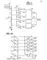
- Parallel analog-to-digital conversion is performed by comparing an analog input signal, indicated by reference numeral 10 in FIG. 1, with each of a plurality of reference levels derived from a common voltage reference 12.
- the reference 12 is connected to a voltage divider 14 to provide a plurality of reference levels, one for each increment in a range from zero to full scale.
- 2 -1 reference levels are obtained from the voltage divider 14 and applied as inputs to an equal number of comparators 16.
- each of the AND gates 24 in the array is typically effected by means of 2 n- 1 AND gates 24, as shown in FIG. 2a or FIG. 2b.
- each of the AND gates 24 in the array is typically effected by means of 2 n- 1 AND gates 24, as shown in FIG. 2a or FIG. 2b.
- each of the AND gates 24 in the array is typically effected by means of 2 n- 1 AND gates 24, as shown in FIG. 2a or FIG. 2b.
- each of the AND gates 24 in the array is typically effected by means of 2 n- 1 AND gates 24, as shown in FIG. 2a or FIG. 2b.
- the AND gates 24 have outputs on lines 26. Each of the lines 18 from the comparators 16 is connected to one of the inputs to a corresponding AND gate. The other input to each AND gate is derived from the next highest level of comparator output and is inverted before application to the AND gate. If the AND gates 24 are considered to be numbered from the bottom (lowest voltage) position to the top, AND gate number i will have an output of C i . C i+1 , where C. is the output from comparator i and the symbol ".” represents a logical AND operation. It will be apparent that if two ones or two zeros are applied to one of the AND gates, a zero output will result.
- a "one" output will be obtained at position i only if the ith comparator output is a one and the (i+l)th comparator output is zero, i.e. at the transition between ones and zeros in the array of comparator outputs.
- the highest level AND gate has only one input, of course, so that if there is a "one” comparator output at that level the "transition” will be shown as occurring at the highest level, indicating a full-scale input signal.
- Operation of the AND gate logic may be controlled by a "convert" signal, indicated at 28, which is applied to each of the comparators 16, over lines 30.
- the convert signal is also applied in inverted form, over lines 32, to enable operation of the AND gates 24.
- each of the AND gates 24' has three inputs, except the uppermost and lowermost ones, which have two inputs each.
- the ith AND gate has one input derived from the ith comparator output and a second input derived from the inverse of the (i+l)th comparator output.
- the third input to each AND gate 24' is derived from the (i-1)th comparator output.
- the output of the ith AND gate is given by the expression C i-1 .Ci. C i+1 , where C i represents the ith comparator output, as before.
- the three-input AND gate arrangement of FIG. 2b requires a comparator output sequence of 1-1-0 in order to indicate a detected transition
- the two-input AND gate arrangement of FIG. 2a requires only a sequence of X-1-0, where the value of X is irrelevant.
- the two-input AND gate transition detection scheme of FIG. 2a is to be preferred, especially when used in conjunction with the present invention.
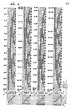
- FIG. 3 shows a conventional encoding technique for converting the transition signal on lines 26 to an eight-bit standard binary signal on output lines 40.
- the encoding logic of FIG. 3 includes four seven-bit latches 41-44, each of which has seven input lines and seven output lines.
- the first sixty-three of the AND gate outputs 26 are selectively connected to the seven inputs of latch 41.
- the AND gate outputs 26 are indicated by numerals 26.1, 26.2, and so forth.
- the solid dots on the intersections of the latch inputs and the AND gate output lines indicate logical OR connections, as do the dots on the intersections between the latch outputs and the eight binary output lines 40.
- intersections of the lines 26 and the inputs to the latch 41 are programmed to load the latch 41 with a binary code equivalent to the position of the AND gate from which the line 26 is derived.
- a "one" on line 26.1 results in a binary code of 0000001 being loaded into latch 41
- a "one” on line 26.2 results in a binary code of 0000010, and so forth.
- the outputs from the latch 41 are connected directly to the corresponding output lines 40. Accordingly, a "one" output on any of the lines 26.1 through 26.63 will result in a corresponding binary code 0000001 through 0111111 being latched into latch 41 and output on the binary output lines 40.
- lines 26.128 through 26.191 are connected to the input lines of latch 43 and lines 26.192 through 26.255 are connected to the input lines of latch 44.
- the input connections for latches 43 and 44 are in fact identical with those of latch 42.
- On the output side of latch 43 however, a "one" output on any of the seven output positions results in an output at the eighth bit position of the output lines 40.
- a "one" output on any of the seven output positions results in an output at the seventh and eighth position of the output lines 40.
- the output code on lines 40 is a standard binary code in the range 00000001 through 11111111, corresponding to inputs on lines 26.1 through 26.255, respectively.
- the result in this example may not be very disturbing, but consider what happens if simultaneous "one" inputs are provided on lines 26.127 and 26.128.
- the combined output on lines 40 is then 11111111, when the correct code should be either 10000000 or 01111111.
- the error is then approximately 100% of the correct value and approximately 50% of the full-scale value.
- Gray code instead of standard binary code reduces the maximum error to only one part in 2 n of full scale for bit separations of one.
- the bit separation is the distance in bit positions between the correct one-to-zero transition point and an incorrect transition point.
- a positive bit separation means that the correct transition point is closer than the incorrect transition point to the zero end of the array of comparator outputs, while a negative bit separation means that the correct transition point is closer to the full-scale end of the array than the incorrect transition.
- Gray code is also effective, but to a lesser degree, in reducing errors caused by transitions spaced by greater than one bit position, there is still room for improvement over the use of Gray code in parallel analog-to-digital converters.
- the conversion from a one-in-(2 n- Ij transition code to a binary code is effected by means of a modified Gray code having the characteristics of Gray code in all but its least significant bit position, which alternates in the same manner as standard binary code.
- a comparison of standard binary code, Gray code and the new code, for decimal values from 0 through 15, is provided in Table 1.
- the converter may also include means for translating from the modified Gray code on lines 40 to standard binary code.
- the translating means is indicated at 50 (FIG. 4), and includes conventional components, such as a decoder and a standard binary encoder.
- the present invention represents a significant advance over parallel analog-to-digital converters of the prior art.
- the invention provides improved performance over Gray code in the conversion from a l-in-(2 n- l) code to a binary code.
- Gray code in the conversion from a l-in-(2 n- l) code to a binary code.
Landscapes
- Engineering & Computer Science (AREA)
- Theoretical Computer Science (AREA)
- Analogue/Digital Conversion (AREA)
- Compression, Expansion, Code Conversion, And Decoders (AREA)
Applications Claiming Priority (2)
| Application Number | Priority Date | Filing Date | Title |
|---|---|---|---|
| US06/525,576 US4591825A (en) | 1983-08-22 | 1983-08-22 | Analog-to-digital-converter and related encoding technique |
| US525576 | 1983-08-22 |
Publications (3)
| Publication Number | Publication Date |
|---|---|
| EP0135290A2 true EP0135290A2 (fr) | 1985-03-27 |
| EP0135290A3 EP0135290A3 (en) | 1988-06-22 |
| EP0135290B1 EP0135290B1 (fr) | 1990-10-31 |
Family
ID=24093811
Family Applications (1)
| Application Number | Title | Priority Date | Filing Date |
|---|---|---|---|
| EP84304845A Expired EP0135290B1 (fr) | 1983-08-22 | 1984-07-16 | Convertisseur analogique-numérique et technique de codage s'y rapportant |
Country Status (4)
| Country | Link |
|---|---|
| US (1) | US4591825A (fr) |
| EP (1) | EP0135290B1 (fr) |
| JP (2) | JPS60100833A (fr) |
| DE (1) | DE3483503D1 (fr) |
Cited By (3)
| Publication number | Priority date | Publication date | Assignee | Title |
|---|---|---|---|---|
| EP0217009A3 (fr) * | 1985-10-04 | 1989-05-03 | Tektronix, Inc. | Encodeur pour la conversion d'un code thermomètre en un code binaire adjacent |
| EP0282147A3 (fr) * | 1987-02-09 | 1990-04-11 | Tektronix Inc. | Circuit de correction d'erreur de convertisseur analogique-numérique |
| US4963874A (en) * | 1987-04-28 | 1990-10-16 | Matsushita Electric Industrial Co., Ltd. | Parallel type A/D converter |
Families Citing this family (14)
| Publication number | Priority date | Publication date | Assignee | Title |
|---|---|---|---|---|
| JPH0681050B2 (ja) * | 1985-08-21 | 1994-10-12 | 株式会社日立製作所 | 並列形ad変換器 |
| US4870417A (en) * | 1988-02-12 | 1989-09-26 | North American Philips Corporation, Signetics Division | Error correction circuit suitable for thermometer or circular code |
| JPH07118656B2 (ja) * | 1988-02-15 | 1995-12-18 | 三菱電機株式会社 | エンコード回路 |
| US5023613A (en) * | 1988-03-31 | 1991-06-11 | Harris Semiconductor Patents, Inc. | Decoder error prevention apparatus for use in flash analog-to-digital converters |
| US4897657A (en) * | 1988-06-13 | 1990-01-30 | Integrated Device Technology, Inc. | Analog-to-digital converter having error detection and correction |
| US5029305A (en) * | 1988-12-21 | 1991-07-02 | Texas Instruments Incorporated | Method and apparatus for error correction in thermometer code arrays |
| US5119098A (en) * | 1989-06-20 | 1992-06-02 | Sony Corporation | Full flash analog-to-digital converter |
| US4928103A (en) * | 1989-09-18 | 1990-05-22 | Analog Devices, Inc. | Parallel analog-to-digital converter using 2.sup.(n-1) comparators |
| JPH03140016A (ja) * | 1989-10-26 | 1991-06-14 | Sharp Corp | A/d変換器 |
| US4975698A (en) * | 1989-12-08 | 1990-12-04 | Trw Inc. | Modified quasi-gray digital encoding technique |
| US5045854A (en) * | 1990-03-01 | 1991-09-03 | Hewlett-Packard Company | Integrated high speed synchronous counter with asynchronous read-out |
| ATE233327T1 (de) * | 1993-03-24 | 2003-03-15 | Georgia Tech Res Inst | Verfahren und vorrichtung zur verbrennungs cvd von filmen und beschichtungen |
| US5382955A (en) * | 1993-11-04 | 1995-01-17 | Tektronix, Inc. | Error tolerant thermometer-to-binary encoder |
| CN109353515B (zh) * | 2018-11-21 | 2023-10-20 | 华南农业大学 | 一种植保无人机液位测量装置 |
Family Cites Families (9)
| Publication number | Priority date | Publication date | Assignee | Title |
|---|---|---|---|---|
| GB849891A (en) * | 1958-04-15 | 1960-09-28 | Standard Telephones Cables Ltd | Improvements in or relating to electric pulse code modulation systems of communication |
| FR1445739A (fr) * | 1965-06-04 | 1966-07-15 | Alcatel Sa | Procédé de codage numérique et ses applications |
| US3560959A (en) * | 1967-03-22 | 1971-02-02 | Us Navy | Readout device for altitude reporting encoder |
| US3518663A (en) * | 1967-09-29 | 1970-06-30 | Singer General Precision | Shaft angle encoder with brush selection logic circuitry |
| JPS4957759A (fr) * | 1972-10-02 | 1974-06-05 | ||
| FR2306575A1 (fr) * | 1975-04-02 | 1976-10-29 | Nadler Morton | Procede et dispositif de conversion de signal electrique analogique en code binaire |
| JPS605097B2 (ja) * | 1977-02-18 | 1985-02-08 | 株式会社日立製作所 | グレイコ−ド発生回路 |
| JPS57204633A (en) * | 1981-06-10 | 1982-12-15 | Toshiba Corp | Analog-to-digital converter |
| US4576543A (en) * | 1983-11-07 | 1986-03-18 | Kmw Products Limited | Knock-down construction for front end loader |
-
1983
- 1983-08-22 US US06/525,576 patent/US4591825A/en not_active Expired - Lifetime
-
1984
- 1984-07-16 EP EP84304845A patent/EP0135290B1/fr not_active Expired
- 1984-07-16 DE DE8484304845T patent/DE3483503D1/de not_active Expired - Fee Related
- 1984-08-22 JP JP59174834A patent/JPS60100833A/ja active Granted
-
1988
- 1988-12-06 JP JP63308699A patent/JPH01188029A/ja active Granted
Cited By (3)
| Publication number | Priority date | Publication date | Assignee | Title |
|---|---|---|---|---|
| EP0217009A3 (fr) * | 1985-10-04 | 1989-05-03 | Tektronix, Inc. | Encodeur pour la conversion d'un code thermomètre en un code binaire adjacent |
| EP0282147A3 (fr) * | 1987-02-09 | 1990-04-11 | Tektronix Inc. | Circuit de correction d'erreur de convertisseur analogique-numérique |
| US4963874A (en) * | 1987-04-28 | 1990-10-16 | Matsushita Electric Industrial Co., Ltd. | Parallel type A/D converter |
Also Published As
| Publication number | Publication date |
|---|---|
| EP0135290A3 (en) | 1988-06-22 |
| EP0135290B1 (fr) | 1990-10-31 |
| US4591825A (en) | 1986-05-27 |
| DE3483503D1 (de) | 1990-12-06 |
| JPH01188029A (ja) | 1989-07-27 |
| JPH0232813B2 (fr) | 1990-07-24 |
| JPH0232815B2 (fr) | 1990-07-24 |
| JPS60100833A (ja) | 1985-06-04 |
Similar Documents
| Publication | Publication Date | Title |
|---|---|---|
| US4591825A (en) | Analog-to-digital-converter and related encoding technique | |
| US5382955A (en) | Error tolerant thermometer-to-binary encoder | |
| US5243348A (en) | Partitioned digital encoder and method for encoding bit groups in parallel | |
| US4978957A (en) | High-speed analog-to-digital converter | |
| EP0070175B1 (fr) | Convertisseur analogique-numérique | |
| US4975698A (en) | Modified quasi-gray digital encoding technique | |
| JPH0253974B2 (fr) | ||
| US6433725B1 (en) | High speed analog-to-digital converter | |
| WO1990001835A1 (fr) | Convertisseur analogique-numerique a risque d'erreurs reduit | |
| US5463395A (en) | Semi-flash type A/D converter employing a correction encoder for eliminating errors in the output signals due to noise, and a corresponding method therefor | |
| US4520347A (en) | Code conversion circuit | |
| US5623265A (en) | Flash analog-to-digital converter and method of operation | |
| CA1338910C (fr) | Systeme de conversion analogique-numerique | |
| US4999630A (en) | Fast analog-digital converter with parallel structure | |
| US7271757B2 (en) | Encoder circuit and A/D conversion circuit | |
| US5252974A (en) | Encoder with error correction particularly for flash analog-to-digital converters | |
| US4970513A (en) | Device for converting an analog signal into a digital signal of a parallel comparison type with error suppression circuits | |
| US5023613A (en) | Decoder error prevention apparatus for use in flash analog-to-digital converters | |
| US6816098B2 (en) | High-speed oversampling modulator device | |
| US3603976A (en) | Modular encoder | |
| US5304994A (en) | Minimal delay leading one detector with result bias control | |
| JP2638002B2 (ja) | 並列型a/d変換器 | |
| SU1198754A1 (ru) | Параллельно-последовательный аналого-цифровой преобразователь | |
| KR20000004486A (ko) | 아날로그/디지탈 변환기 | |
| KR100787078B1 (ko) | 인코더 회로 및 a/d 변환 회로 |
Legal Events
| Date | Code | Title | Description |
|---|---|---|---|
| PUAI | Public reference made under article 153(3) epc to a published international application that has entered the european phase |
Free format text: ORIGINAL CODE: 0009012 |
|
| AK | Designated contracting states |
Designated state(s): DE FR GB IT NL |
|
| PUAL | Search report despatched |
Free format text: ORIGINAL CODE: 0009013 |
|
| AK | Designated contracting states |
Kind code of ref document: A3 Designated state(s): DE FR GB IT NL |
|
| 17P | Request for examination filed |
Effective date: 19880803 |
|
| 17Q | First examination report despatched |
Effective date: 19890817 |
|
| ITF | It: translation for a ep patent filed | ||
| GRAA | (expected) grant |
Free format text: ORIGINAL CODE: 0009210 |
|
| AK | Designated contracting states |
Kind code of ref document: B1 Designated state(s): DE FR GB IT NL |
|
| REF | Corresponds to: |
Ref document number: 3483503 Country of ref document: DE Date of ref document: 19901206 |
|
| ET | Fr: translation filed | ||
| PLBE | No opposition filed within time limit |
Free format text: ORIGINAL CODE: 0009261 |
|
| STAA | Information on the status of an ep patent application or granted ep patent |
Free format text: STATUS: NO OPPOSITION FILED WITHIN TIME LIMIT |
|
| 26N | No opposition filed | ||
| PGFP | Annual fee paid to national office [announced via postgrant information from national office to epo] |
Ref country code: GB Payment date: 19930705 Year of fee payment: 10 |
|
| PGFP | Annual fee paid to national office [announced via postgrant information from national office to epo] |
Ref country code: FR Payment date: 19930709 Year of fee payment: 10 |
|
| ITTA | It: last paid annual fee | ||
| PGFP | Annual fee paid to national office [announced via postgrant information from national office to epo] |
Ref country code: NL Payment date: 19930731 Year of fee payment: 10 |
|
| PGFP | Annual fee paid to national office [announced via postgrant information from national office to epo] |
Ref country code: DE Payment date: 19930825 Year of fee payment: 11 |
|
| PG25 | Lapsed in a contracting state [announced via postgrant information from national office to epo] |
Ref country code: GB Effective date: 19940716 |
|
| PG25 | Lapsed in a contracting state [announced via postgrant information from national office to epo] |
Ref country code: NL Effective date: 19950201 |
|
| GBPC | Gb: european patent ceased through non-payment of renewal fee |
Effective date: 19940716 |
|
| NLV4 | Nl: lapsed or anulled due to non-payment of the annual fee | ||
| PG25 | Lapsed in a contracting state [announced via postgrant information from national office to epo] |
Ref country code: FR Effective date: 19950331 |
|
| REG | Reference to a national code |
Ref country code: FR Ref legal event code: ST |
|
| PG25 | Lapsed in a contracting state [announced via postgrant information from national office to epo] |
Ref country code: DE Effective date: 19960402 |