EP0135302A1 - Verfahren und Apparatur zur Untersuchung von gedruckten Schaltungen - Google Patents
Verfahren und Apparatur zur Untersuchung von gedruckten Schaltungen Download PDFInfo
- Publication number
- EP0135302A1 EP0135302A1 EP84304973A EP84304973A EP0135302A1 EP 0135302 A1 EP0135302 A1 EP 0135302A1 EP 84304973 A EP84304973 A EP 84304973A EP 84304973 A EP84304973 A EP 84304973A EP 0135302 A1 EP0135302 A1 EP 0135302A1
- Authority
- EP
- European Patent Office
- Prior art keywords
- track
- board
- signals
- output
- areas
- Prior art date
- Legal status (The legal status is an assumption and is not a legal conclusion. Google has not performed a legal analysis and makes no representation as to the accuracy of the status listed.)
- Granted
Links
Images


Classifications
-
- G—PHYSICS
- G06—COMPUTING OR CALCULATING; COUNTING
- G06T—IMAGE DATA PROCESSING OR GENERATION, IN GENERAL
- G06T7/00—Image analysis
- G06T7/0002—Inspection of images, e.g. flaw detection
- G06T7/0004—Industrial image inspection
- G06T7/0006—Industrial image inspection using a design-rule based approach
-
- G—PHYSICS
- G01—MEASURING; TESTING
- G01N—INVESTIGATING OR ANALYSING MATERIALS BY DETERMINING THEIR CHEMICAL OR PHYSICAL PROPERTIES
- G01N21/00—Investigating or analysing materials by the use of optical means, i.e. using sub-millimetre waves, infrared, visible or ultraviolet light
- G01N21/84—Systems specially adapted for particular applications
- G01N21/88—Investigating the presence of flaws or contamination
- G01N21/95—Investigating the presence of flaws or contamination characterised by the material or shape of the object to be examined
- G01N21/956—Inspecting patterns on the surface of objects
-
- G—PHYSICS
- G06—COMPUTING OR CALCULATING; COUNTING
- G06T—IMAGE DATA PROCESSING OR GENERATION, IN GENERAL
- G06T2207/00—Indexing scheme for image analysis or image enhancement
- G06T2207/30—Subject of image; Context of image processing
- G06T2207/30108—Industrial image inspection
- G06T2207/30141—Printed circuit board [PCB]
Definitions
- This invention relates to a method and apparatus for inspecting a pattern on a substrate such as a pattern on a printed wiring board.
- a reduction in the effective width of a printed wiring conductor can be caused by a nick or pinhole in the conductor at a point or points along the conductor as well as by a length of narrow conductor due to faulty processing or design.
- One well known apparatus for testing boards electrically is the tracking or "bed of nails" tester. Such apparatus can check the continuity between the various connection points on a board but is unable to detect nicks, pinholes, regions of narrow track, or partial bridges which can occur if the spacing between adjacent conductors is too small. Such apparatus also require expensive tooling to enable them to be used in the inspection of a wide range of boards.
- apparatus for testing a printed wiring board comprising means for optically scanning a board to J e tested in two orthogonal, X-Y axes such that for each scan in the Y direction it scans a narrow strip of the board of predetermined width, w, in the X direction, the scanning means being arranged to provide n.m discrete signals for each scan in the Y direction, wherein n is a predetermined number of signals
- the datum areas may comprise conductive material surrounding holes in the board such that at the end of a test the stored information is equivalent to a wiring list of interconnected datum areas.
- the datum areas may comprise edge connector areas.
- the processing means may comprise means for comparing the stored signals with a plurality of signals representative of the required interconnections for the board (the required wiring list) thereby to test the quality of the board.
- the apparatus may comprise track contraction means for processing preselected areas of each group of nl x ml signals in such a manner as to determine whether the width of a conductor at any point along it's length is less than a predetermined minimum width.
- the apparatus may further comprise track expansion means arranged to process the scanned signals in such a manner as to determine whether the spacing between adjacent conductors at any point along their length is less than a predetermined value.
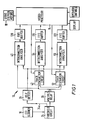
- Fig 1 there is shown an apparatus 10 for testing the wiring of a printed wiring board 12 (Figs 2 & 3).
- the apparatus 10 is controlled by a microcomputer 14 which also includes various storage elements such as random access memories (RAM's) for use in the operation of the apparatus and the storage of information for use in testing a board 12.
- RAM's random access memories
- the apparatus 10 comprises an optical scanner 16 which is controlled by servo/stepper motors 18 to traverse backwards and forwards across the surface of the board 12 in the Y direction and after each traversal it is i moved relative to the board a predetermined distance in the X direction.
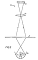
- Fig 2 shows a simple arrangement for such a scanner 16, in which the optical scanning device 20 can be traversed backwards and forwards in the Y direction while the board 12 can be stepped a discrete distance in the K direction between each Y traversal.
- the board 12 could be moved on an X-Y table noveable in both orthogonal axes with the device 20 fixed in position or the board 12 could be mounted in a fixed position and the scanning device 20 mounted for movement in the X-Y directions.
- Fig 3 shows a simplified side view of an optical scanning device 20, utilising a charge coupled device (CCD) camera 22 such as one sold by Fairchild under type No. CD1300R.
- CCD charge coupled device
- Light from a tungsten-halogen lamp 24 is concentrated by an ellipsoidal reflector 26 onto the underside of the board.
- the light reaches the board at a very wide range of angles, and can diffuse quite a long way sideways, so that power supply tracks on the board 12, for example do not completely block out the rear illumination.
- the board 12 could be scanned with a retroreflective scanner using either conventional tungsten-halogen or laser light and the reflected light detected to distinguish track areas from non-track areas and from holes without changing any of the principles herein described.
- the front surface of the board is imaged by a standard camera or enlarger lens 32 onto a charge-coupled device 22, which contains a linear array of photosites together with circuitry for reading out the light levels from each photosite.
- each photosite is responsive to a 20 micron X 20 micron area (a pixel).
- the linear array of photosites effectively produces a parallel output containing 1024 analogue pieces of information in the X direction.
- the array continues to develop 1024 output signals at discrete positions 20 microns apart for the complete scan in the Y direction.
- the 1024 signals from the CCD scanner device 16 representing a strip 20mm long in the X direction and 20 microns wide in the Y direction are coupled serially to the input of a dual threshold circuit 34 having a first, lower threshold reference voltage input and a second, higher threshold reference voltage input.
- the circuit 34 distinguishes between track (ie conductor), non-track (ie insulating substrate) and holes by comparing each input signal with the two threshold levels. If the input signal from the scanner 16 is less than the first threshold voltage the circuit produces a logic signal '1' indicative of track area on output 34b; if it is greater than the second threshold voltage the circuit 34 produces a logic signal '1' on the output 34a indicative of a hole in the board and if the input signal has a level equal to or between the first and second threshold levels it produces a logic signal '0' indicative of a non-track area on output 34b. These input signals are coupled to the circuit 34 at a 10 MHz clock rate.
- the binary stream of information indicative of track and non-track pixel areas appearing at output 34b is fed to a multiple delay circuit 36.
- the circuit 36 is implemented using random access memories (RAM's) for low cost, but can be considered conceptually, and for ease of description, as a set of shift registers 38 each one of which feeds the next as shown in Fig 4.
- RAM's random access memories
- the parallel outputs 39a to 39m' of the shift registers 38a to 38m' at any time can be regarded as m' bits of information in a row in the Y direction of scan.
- the outputs of the shift registers represent a parallel scan across the width of the scan, as shown in part in the table of Fig 5.
- the parallel output signals from the multiple delay circuit 36 that is the outputs 39a to 39m' are coupled in parallel to a pair of circuits 42, 52 whose function is to determine for each point in the scanned image whether it is within a preset distance of a track or non-track area.
- the circuit 42 is called a track contraction circuit and the circuit 52 a track expansion circuit; the track expansion circuit 52 is similar to the track contraction circuit 42 with the exception that it's input and output signals are inverted. Any one of the outputs of the multiple delay circuit 36 (for preferance the middle one of the 39a to 39m') is also fed to the interconnection analyser 40.
- the interconnection analyser 40 is coupled through a first-in, first-out buffer 120 to the microcomputer 14. It's function is to produce a set of signals to be stored which are a representation of a wiring diagram for the printed wiring board 12, that is it provides a set of X-Y coordinate signals representative of holes in the board and edge connector areas, if any, labelled to indicate which holes/edge connector areas are interconnected.
- the track contraction circuit 42 will now be described with reference to Fig 6.
- the circuit 42 comprises a plurality of tapped shift registers 44a to 44m' having inputs 45a to 45m' coupled to the outputs 39a to 39m' respectively of the shift registers 38.
- Each circuit 44 has a programmable, tapped output 46a to 46m' which is coupled to the preset input 47a to 47m' of a presettable down counter 48a to 48m' respectively.
- the taps on the shift registers 44 are under the control of the microprocessor 14.
- the contraction circuit 42 is arranged to determine whether or not all of the bits in the shift registers 44 which would fit in a circle of radius R, where R is equal to half the minimum specified track width, are a binary '1' to indicate track.
- the value of R is predetermined for the board 12 and it's value is set into the computer by the operator.
- the value of R could be made equal to 20 and it would be possible to look at the bits of the individual cells of the shift registers to determine their value. If each cell was provided with an output an individual AND gate could be coupled to various cells in a particular shift register and the outputs of the individual AND gates coupled to the inputs of another AND gate so that if, and only if, all of the individual cells contained a binary '1' then the output of the final AND gate would be a '1' to indicate a complete track in the area of radius R. However if only a single cell was set to '0' then the output of the final AND gate would be zero indicating that the track was not entirely complete at the area being tested at that instant in time.
- each forty bits long the first and fortieth shift registers could be tapped at, say cells 20 and 21, the middle twentieth and twenty first shift registers could have every cell tapped and connected to an associated input of two forty input AND gates.
- the shift registers two to nineteen would have progressively more cells tapped and the registers twenty-two to thirty-nine would have progressively fewer cells tapped so that the outputs from the tapped cells would approximate to a circle of radius R.
- this arrangement would be expensive in AND gates and quite complex and somewhat difficult to vary in practice and the circuit of Fig 6 was devised.
- the taps on the shift registers 44 can be set automatically by the microcomputer 14 under the control of the operator and it will be seen that they are variable delays, the delay being a maximum (20 bits) for the first and fortieth shift registers 44 and a minimum (zero) for, say, the twentieth and twenty-first.
- the delays for shift registers 2 to 19 decrease progressively from 19 to 1 bits and for shift registers 22 to 39 increase progressively from 1 to 19 bits.
- the counters 48a to 48m' can be preset to a count determined by it's position, ie for the first and fortieth counters the preset count would be a minimum value (say 1 or 2) and for the twentieth and twenty-first counters to a maximum value (say 40).
- the other counters are preset to values increasing and decreasing in the same way as the delays through the shift registers 44 decrease and increase.
- Fig 7 is a diagramatic representation of a simplified circuit of Fig 6 having nine preset shift registers 44 each nine bits long.
- the circuitry is determining whether there are any non-track areas within a distance R from the point P.
- Each circuit 44,48 determines whether there are any non-track areas along a corresponding strip such as that marked XXXXXX and the outputs of all of the counters 48 are combined in AND gate 50 to provide a single output; '1' if all of the counter outputs indicate track; '0' if any one or more of the counter outputs indicate the presence of a non-track area.
- the seventh counter 48g would be preset to a count of seven whenever a non-track element is seen at position Q7.
- the counter is then counted down to zero so that if all of the elements marked X contain track, ie are at '1' then the output of the counter will go to '1'.
- the output of AND gate 50 will thus go high '1' if and only if all of the elements within a distance R of P contain track.
- the output of the AND gate is thus a serial representation of an image similar to that arriving at the threshold circuit 34, except that it has been delayed, and the track areas have been
- the track expansion circuit 52 is similar to the track contraction circuit 42 with the exception that the input to it and the output from it are inverted. It is thus caused to consider track as non-track and vice versa. In this case if the value R is made half the minimum allowable spacing between conductors then if the spacing is adequate the output of it's AND gate (equivalent to AND gate 50) will be a series of '1's but if the spacing at any position on the board is less than the minimum allowable the output of the AND gate will go to '0'.
- the information from the track expansion circuit will be processed in an interconnection analyser 56 and the output fed to the microcomputer 14 via the FIFO buffer 122.
- the function of the interconnection analyser is to determine which holes, and edge connector areas if any, are connected together to form a wiring list which is stored in the computer.
- edge connector areas are designated as holes but are identifiable as edge connectors by their X-Y coordinates.
- the wiring lists compiled by the circuits 54, 56 ie the "thinned” and “fattened” images respectively, should be the same but if there are any narrow cuts, nicks, pinholes or inadaquate spacing between conductors the two wiring lists will differ. They can also be compared with a wiring list obtained from a photographic or other artwork prepared for the board or from a known good board. Alternatively, or in addition they can be compared with a wiring list prepared from the interconnection analyser 40 which, in effect provides a basic list of the various complete interconnections but regardless of the presence of nicks, pinholes or the like, provided that the circuit is complete and regardless of the spacing between conductors provided that they do not actually touch.
- the interconnection analysers 54, 56 scan the data streams from the track contraction circuit 42 and the track expansion circuits 52 respectively and associate a "label" with each track area. These labels are binary numbers which are allocated in sequence whenever a "new" piece of track is scanned. When a hole or termination regarded as a hole is detected in the board, the label of the corresponding piece of track is passed to the microprocessor together with the coordinates of the.hole. When two pieces of track which have been given different labels converge, so that they are known to be connected together, the two labels concerned are passed to the microprocessor with the information that they are interconnected.
- the edge of a band 1024 bits wide X m bits long is defined by the final, or 1024th, bit in each 1024 bits across the width w of the band.
- the labels for the edge of a band 1024 bits wide being scanned are held in a special store (edge RAM) so that they can be used to relate each band to the next succeeding band adjacent to it.
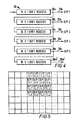
- the labelling process is carried out in three stages as illustrated in the tables of Figs. 8, 9, 10 & 11.
- the lower line represents labels that have been determined for the previous scan line
- the upper line represents the labels that have been determined so far for the scan line that is currently being labelled.
- the data for this scan line is traversed three times before all the labels are correctly allocated. The first traversal is from right to left, and serves only to identify any region of track which does not touch any regions of track in the previous line, and which will therefore require a new label to be allocated to it.
- the lower line shows part of a scanned Line which has been labelled and, reading from left to right, the first track areas have been labelled as track areas 27, from the edge RAM, the 1 ext three areas are non-track, the next two areas have been labelled as track areas 35 and so on.
- the labels are allocated by a label allocation counter (Fig 16) and are coupled as 16 bit words to the microprocessor 14 when either a hole or an edge connector on the board 12 are detected, along with the X-Y coordinates of that feature, and when a "collision" (to be defined hereinafter) occurs.
- the leftmost digit, 27, is stored in an "edge" RAM which identifies the labels allocated to areas of track along the edge of the previously scanned 20mm wide band. This facilitates identification of the edges of each subsequent band as it is scanned.
- the upper line of Fig 8 shows the leftmost digit 27 allocated to the first track area, because it represents an edge of the scanning line and could be numbered by reference to the "edge RAM".
- the remainder of the line merely shows areas of non-track and track to which labels are to be allocated.
- the first label allocation traversal is from right to left as shown in Fig 9 and, as mentioned, serves to identify areas of track which do not touch any areas of track in the lower, immediately proceeding scanned track.
- a label allocation request A in the first non-track area that occurs after that particular piece of track.
- Fig 9 there are two such adjacent areas at positions 10 and 11 from the left. As the data is being traversed from right to left the first available non-track area is position 9 and this is allocated a label allocation request A as shown.
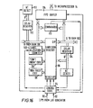
- Fig 14 input data in serial form and representing the 1024 bits of information of a scanned line is coupled from the output of the track contraction circuit 42 to an input 70 of the interconnection analyser 54.
- a similar circuit to that of Fig 14 is used in the interconnection analysers 40 and 56 and so the operation in relation to these circuits will not be discussed in detail.
- the output of the 1024 bit delay 72 and the AND gate 80 are coupled to reset and set inputs 82a, 82b of a bistable circuit 82.
- current data bits corresponding to the track/non-track areas in the upper row of Fig 9 are coupled to the set input 82b of the bistable circuit 82 and the corresponding data from areas in the previous scan line are fed to the reset input 82a of the bistable circuit 82.
- the AND gate 80 So long as the input data is representative of non-track ie '0' the AND gate 80 has a'0' on input 80a and a '0' on the line to input 80b due to the 1-bit delay through delay 74 which is inverted to present a '1' input to the AND gate 80.
- the AND gate 80 to provide a '1' on the input 82b to set the bistable circuit 82, which provides a '1' at the output 82c. If the next piece of input data is a '1' representative of track the input at 80a is a '1' but the previous '1' input delayed 1-bit arrives at the input 80b is inverted and the output of AND gate 80 returns to "zero".
- the delay circuit 72 being 1024 bits long is effectively providing information about the area of track immediately below the area currently being examined. If the area in the lower row is also track then a '1' will be applied to the reset input of bistable 82 to reset it's output to '0'. However if the output of the delay 72 is '0' representing non-track then the bistable will remain set and a '1' will be applied to input 84a of AND gate 84. However, while the input 70 is receiving track signals the '1' signals fed to inverting input 78a keep the output of AND gate 78 at '0' and thus inhibit the AND gate 84.
- bistable 82 remains set but can be reset if a '1' appears at input 82a.
- the input signal at 70 reverts to non-track '0' and this coupled to inverting input 78a of AND gate 78 removes the inhibit signal from AND gate 84 and allows a '1' into the label allocation request store 86. This is shown as A in Fig 9 and as aforementioned appears in the first non-track area after a piece of track to which a label has not been allocated.
- the data store 76 contains the 1024 bits of information of the scanned line and the LAR store 86 contains a series of '0' and a '1' at the position immediately to the left of an isolated piece of track to which a label has not been allocated and which is not adjacent to a piece of track in the line previously scanned.
- the stores 76, 86 are bidirectional so that data can be read out from left to right during the next traversal (Fig 10) so that at position 9 from the left a label allocation request is fed from store 86 to a label allocation counter (to be described in relation to Figs 12 and 16) which allocate a new label, in this case 57, to the track areas 10 and 11 from the left and updates the label allocation counter to the next label to be allocated.
- the track areas are labelled up as far as possible by reference to the labels in adjacent elements. Some elements may be impossible to label at this stage, and they are identified by a special 'Don't Know' code, so that they can be resolved during the third traversal, for example the track at position 6 from the left in Fi g . 10 because it is adjacent to an area of non-track in the previous line immediately below it.
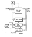
- the labels for the previous scan line are held in a RAM 108 marked RAM 1-in Fig. 15, and the left-right traversal circuit' uses these to generate a set of labels including 'Don't Knows' in the RAM 100 marked RAM 2 in Fig. 15. during the third traversal these values are transferred back to RAM 1 by the 'right-left traversal circuit' Fig. 17 which also replaces any 'Don't Knows' by the correct labels.
- the output from the 1,024 bit data store 76 is coupled to a data input terminal 90 of circuit Fig. 16.
- the output from the label allocation request (LAR) Store 86 being a series of '0' but containing a '1' for each new label to be allocated is coupled to input terminal 92 of Fig. 16.
- Non-track elements are labelled with 'non-track' code. If a 'label allocation request' code is encountered, a new label is obtained from the label allocation counter (Fig 16). Other elements are labelled by reference to the adjacent elements. In the situations shown below the element marked ? is a track element which is to be labelled, L1 & L2 are differing labels and a 0 represents a non-track element.
- the various possibilities are as follows:
- data input is coupled to input 90 and label allocation request input is coupled to input 92.of a control logic circuit 94.
- the input is track then it is interrogated (B) to determine whether there is also a label allocation request signal on input 92. If there is, the logic circuit 94 couples the output of a label allocation counter 102 to the RAM 100, and then increments the counter 102 to the next label address.
- the interconnection analysers 40 and 56 operate in a similar way to that of the analyser 54 but the data input in the case of analyser 56 is, in effect, the data after "track expansion" as hereinbefore described and in the case of analyser 40 it is unmodified data.
- the function of the hole detection circuit 35 Fig 18 is to generate a single pulse when the input data stream from threshold circuit 34 Fig 1 corresponds to the centre of a hole in the board 12. Since this hole appears to the threshold circuit as a non-track area, there will be no label corresponding to the centre of the hole.
- An additional register 124 Fig 17 is therefore provided which is connected to the output of the interconnection analyser but is clocked only when the label detect circuit 126 detects a label. This register will therefore contain the last label before the hole was encountered and this label is sent via the FIFO buffer 128 Fig 17 to the microprocessor 14 together with the hole coordinates when the hole detection circuit 35 generates a pulse.
- the hole detection circuit is shown in Fig 18.
- the 'expansion circuit' 130 shown in this figure is identical to that used for track expansion, and is set to a radius R' slightly greater than the nominal hole size. initially it's input and output signals are both zero.
- R' slightly greater than the nominal hole size.
- the output 130b from the expansion circuit 130 will correspond to a circle slightly larger than the hole, and centered on it.
- This output is inverted and gated with the input signal at AND gate 134, and therefore serves to suppress all further signals generated by that hole.
- the single one bit that was generated when the hole was first encountered is delayed in the Rn bit delay 132 to bring it to the centre of the hole, and passed to the interconnection analysers 40,54 and 56.
- the information fed to the microprocessor from the interconnection analyser 40 via the FIFO buffer 120 is sufficient to enable a wiring list to be generated indicating which holes are connected to which other holes, and this can be compared with the wiring list obtained from a known good board so that differences between the two can be indicated to the operator in the same way as with a 'bed-of-nails' tester.
- the wiring lists obtained for the 'thinned' and 'fattened' images by way of analysers 54 and 56 and their respective FIFO buffers 114 and 122 can also be compared to determine the presence of partial breaks and shorts.
- a procedure for determining the wiring list is as follows:
Landscapes
- Engineering & Computer Science (AREA)
- Physics & Mathematics (AREA)
- General Physics & Mathematics (AREA)
- Biochemistry (AREA)
- Immunology (AREA)
- Theoretical Computer Science (AREA)
- Health & Medical Sciences (AREA)
- Life Sciences & Earth Sciences (AREA)
- Chemical & Material Sciences (AREA)
- Analytical Chemistry (AREA)
- Quality & Reliability (AREA)
- General Health & Medical Sciences (AREA)
- Computer Vision & Pattern Recognition (AREA)
- Pathology (AREA)
- Investigating Materials By The Use Of Optical Means Adapted For Particular Applications (AREA)
- Printing Elements For Providing Electric Connections Between Printed Circuits (AREA)
- Length Measuring Devices By Optical Means (AREA)
- Length Measuring Devices With Unspecified Measuring Means (AREA)
- Image Processing (AREA)
- Image Analysis (AREA)
- Tests Of Electronic Circuits (AREA)
Priority Applications (1)
| Application Number | Priority Date | Filing Date | Title |
|---|---|---|---|
| AT84304973T ATE33314T1 (de) | 1983-07-25 | 1984-07-20 | Verfahren und apparatur zur untersuchung von gedruckten schaltungen. |
Applications Claiming Priority (2)
| Application Number | Priority Date | Filing Date | Title |
|---|---|---|---|
| GB8320016 | 1983-07-25 | ||
| GB838320016A GB8320016D0 (en) | 1983-07-25 | 1983-07-25 | Apparatus for inspecting printed wiring boards |
Publications (2)
| Publication Number | Publication Date |
|---|---|
| EP0135302A1 true EP0135302A1 (de) | 1985-03-27 |
| EP0135302B1 EP0135302B1 (de) | 1988-03-30 |
Family
ID=10546253
Family Applications (1)
| Application Number | Title | Priority Date | Filing Date |
|---|---|---|---|
| EP84304973A Expired EP0135302B1 (de) | 1983-07-25 | 1984-07-20 | Verfahren und Apparatur zur Untersuchung von gedruckten Schaltungen |
Country Status (6)
| Country | Link |
|---|---|
| US (1) | US4635289A (de) |
| EP (1) | EP0135302B1 (de) |
| JP (1) | JPS6095309A (de) |
| AT (1) | ATE33314T1 (de) |
| DE (1) | DE3470226D1 (de) |
| GB (1) | GB8320016D0 (de) |
Cited By (9)
| Publication number | Priority date | Publication date | Assignee | Title |
|---|---|---|---|---|
| EP0228963A2 (de) | 1985-12-27 | 1987-07-15 | AT&T Corp. | Untersuchungssystem durch Linienabtastung für Schaltungsplatten |
| EP0275721A1 (de) * | 1987-01-20 | 1988-07-27 | Up Systems | Automatisches Verfahren zur zeilenweisen optischen Analyse und elektronischen Prüfung des Musters einer zweidimensionalen Szene durch Gestaltfolgung |
| EP0206713A3 (de) * | 1985-06-17 | 1988-08-24 | Visionetics Corporation | Grobfehler-Detektor zur Überprüfung von gedruckten Schaltungen |
| EP0209252A3 (de) * | 1985-07-15 | 1988-09-21 | Visionetics Corporation | Detektor für kleine Fehlstellen in gedruckten Schaltungskarten |
| EP0206709A3 (de) * | 1985-06-17 | 1988-09-28 | Visionetics Corporation | Automatische optische Überprüfung für gedruckte Schaltungen |
| FR2640812A1 (fr) * | 1988-12-16 | 1990-06-22 | Juki Kk | Appareil et procede d'ecriture directe |
| EP0493657A3 (en) * | 1990-12-31 | 1992-08-05 | Beltronics, Inc. | Method and apparatus for identifying manufacturing defects in solid state devices |
| EP0488188A3 (de) * | 1990-11-27 | 1992-12-30 | Dainippon Screen Mfg. Co., Ltd. | Verfahren und Vorrichtung zum Inspektieren der Breite der Linien einer gedruckten Schaltung |
| EP0488206A3 (en) * | 1990-11-27 | 1994-06-15 | Dainippon Screen Mfg | Method of and apparatus for inspecting pattern on printed board |
Families Citing this family (21)
| Publication number | Priority date | Publication date | Assignee | Title |
|---|---|---|---|---|
| US4953224A (en) * | 1984-09-27 | 1990-08-28 | Hitachi, Ltd. | Pattern defects detection method and apparatus |
| US4881269A (en) * | 1985-07-29 | 1989-11-14 | French Limited Company - Centaure Robotique | Automatic method of optically scanning a two-dimensional scene line-by-line and of electronically inspecting patterns therein by "shape-tracking" |
| US4811409A (en) * | 1985-09-12 | 1989-03-07 | Insystems, Inc. | Method and apparatus for detecting defect information in a holographic image pattern |
| DE3540100A1 (de) * | 1985-11-12 | 1987-06-11 | Mania Gmbh | Verfahren zur optischen pruefung von leiterplatten |
| JPS62127987A (ja) * | 1985-11-28 | 1987-06-10 | Yokogawa Electric Corp | プリント板パタ−ン検査方法 |
| JPS62209305A (ja) * | 1986-03-10 | 1987-09-14 | Fujitsu Ltd | 寸法良否判定方法 |
| ATE43716T1 (de) * | 1986-03-19 | 1989-06-15 | Rollei Fototechnic Gmbh | Verfahren zur photogrammetrischen erfassung eines objektes mit hilfe zumindest eines optoelektrischen festkoerper-flaechensensors. |
| JPS63179203A (ja) * | 1987-01-20 | 1988-07-23 | Hiyuutec:Kk | コ−ナ−位置検出装置 |
| EP0341944A3 (de) * | 1988-05-10 | 1991-06-26 | Gec Plessey Telecommunications Limited | Verfahren und Vorrichtungen zur Positionserfassung |
| US5027417A (en) * | 1989-03-31 | 1991-06-25 | Dainippon Screen Mfg. Co., Ltd. | Method of and apparatus for inspecting conductive pattern on printed board |
| DE69124288T2 (de) * | 1990-05-30 | 1997-05-07 | Dainippon Screen Mfg | Verfahren zum Lesen einer optischen Abbildung einer untersuchten Oberfläche und dafür einsetzbare Bildleseeinrichtung |
| US5184217A (en) * | 1990-08-02 | 1993-02-02 | Doering John W | System for automatically inspecting a flat sheet part |
| IL99823A0 (en) * | 1990-11-16 | 1992-08-18 | Orbot Instr Ltd | Optical inspection method and apparatus |
| DE69331433T2 (de) * | 1992-10-22 | 2002-10-02 | Advanced Interconnection Technology, Inc. | Einrichtung zur automatischen optischen Prüfung von Leiterplatten mit darin verlegten Drähten |
| US6066845A (en) * | 1997-11-14 | 2000-05-23 | Virtek Vision Corporation | Laser scanning method and system |
| JP4188558B2 (ja) * | 1997-11-14 | 2008-11-26 | ヴァーテック ヴィジョン コーポレイション | レーザ走査方法およびシステム |
| GB2362459A (en) * | 2000-05-16 | 2001-11-21 | Lloyd Doyle Ltd | Method and apparatus for inspection of printed wiring boards |
| US6700658B2 (en) | 2001-10-05 | 2004-03-02 | Electro Scientific Industries, Inc. | Method and apparatus for circuit pattern inspection |
| JP4242796B2 (ja) * | 2004-03-12 | 2009-03-25 | パナソニック株式会社 | 画像認識方法及び画像認識装置 |
| US10759670B2 (en) | 2017-09-11 | 2020-09-01 | Ionic Solutions Ltd. | Apparatus and process for the production of soda ash |
| CN115112086B (zh) * | 2022-05-30 | 2023-06-02 | 广州广芯封装基板有限公司 | 一种线路板的涨缩测试方法 |
Citations (2)
| Publication number | Priority date | Publication date | Assignee | Title |
|---|---|---|---|---|
| US4037941A (en) * | 1975-06-30 | 1977-07-26 | International Business Machines Corporation | Inspection tool |
| DE2700252A1 (de) * | 1977-01-05 | 1978-07-06 | Licentia Gmbh | Verfahren zum pruefen definierter strukturen |
Family Cites Families (9)
| Publication number | Priority date | Publication date | Assignee | Title |
|---|---|---|---|---|
| JPS6122254B2 (de) * | 1974-01-30 | 1986-05-30 | Hitachi Ltd | |
| JPS5379571A (en) * | 1976-12-24 | 1978-07-14 | Hitachi Ltd | Pattern inspecting apparatus |
| JPS5915381B2 (ja) * | 1978-10-16 | 1984-04-09 | 日本電信電話株式会社 | パタ−ン検査法 |
| JPS56118187A (en) * | 1980-02-25 | 1981-09-17 | Hitachi Ltd | Counter circuit of two dimensional pattern |
| JPS57108606A (en) * | 1980-12-26 | 1982-07-06 | Hitachi Ltd | Automatic appearance inspection apparatus |
| US4479145A (en) * | 1981-07-29 | 1984-10-23 | Nippon Kogaku K.K. | Apparatus for detecting the defect of pattern |
| US4500202A (en) * | 1982-05-24 | 1985-02-19 | Itek Corporation | Printed circuit board defect detection of detecting maximum line width violations |
| EP0095517B1 (de) * | 1982-05-28 | 1985-11-21 | Ibm Deutschland Gmbh | Verfahren und Einrichtung zur automatischen optischen Inspektion |
| US4541114A (en) * | 1983-05-05 | 1985-09-10 | Research Environmental/Institute of Michigan | Routing techniques using serial neighborhood image analyzing system |
-
1983
- 1983-07-25 GB GB838320016A patent/GB8320016D0/en active Pending
-
1984
- 1984-07-20 DE DE8484304973T patent/DE3470226D1/de not_active Expired
- 1984-07-20 AT AT84304973T patent/ATE33314T1/de not_active IP Right Cessation
- 1984-07-20 EP EP84304973A patent/EP0135302B1/de not_active Expired
- 1984-07-23 US US06/633,436 patent/US4635289A/en not_active Expired - Lifetime
- 1984-07-25 JP JP59155101A patent/JPS6095309A/ja active Pending
Patent Citations (2)
| Publication number | Priority date | Publication date | Assignee | Title |
|---|---|---|---|---|
| US4037941A (en) * | 1975-06-30 | 1977-07-26 | International Business Machines Corporation | Inspection tool |
| DE2700252A1 (de) * | 1977-01-05 | 1978-07-06 | Licentia Gmbh | Verfahren zum pruefen definierter strukturen |
Non-Patent Citations (1)
| Title |
|---|
| PROCEEDINGS OF THE FOURTH INTERNATIONAL JOINT CONFERENCE ON PATTERN RECOGNITION, November 1978, Kyoto, JP; N. GOTO et al. "An automatic inspection system for mask patterns", pages 970-974 * |
Cited By (12)
| Publication number | Priority date | Publication date | Assignee | Title |
|---|---|---|---|---|
| EP0206713A3 (de) * | 1985-06-17 | 1988-08-24 | Visionetics Corporation | Grobfehler-Detektor zur Überprüfung von gedruckten Schaltungen |
| EP0206709A3 (de) * | 1985-06-17 | 1988-09-28 | Visionetics Corporation | Automatische optische Überprüfung für gedruckte Schaltungen |
| EP0209252A3 (de) * | 1985-07-15 | 1988-09-21 | Visionetics Corporation | Detektor für kleine Fehlstellen in gedruckten Schaltungskarten |
| EP0228963A2 (de) | 1985-12-27 | 1987-07-15 | AT&T Corp. | Untersuchungssystem durch Linienabtastung für Schaltungsplatten |
| EP0228963A3 (en) * | 1985-12-27 | 1988-07-13 | American Telephone And Telegraph Company | Linescan inspection system for circuit boards |
| EP0275721A1 (de) * | 1987-01-20 | 1988-07-27 | Up Systems | Automatisches Verfahren zur zeilenweisen optischen Analyse und elektronischen Prüfung des Musters einer zweidimensionalen Szene durch Gestaltfolgung |
| FR2640812A1 (fr) * | 1988-12-16 | 1990-06-22 | Juki Kk | Appareil et procede d'ecriture directe |
| EP0488188A3 (de) * | 1990-11-27 | 1992-12-30 | Dainippon Screen Mfg. Co., Ltd. | Verfahren und Vorrichtung zum Inspektieren der Breite der Linien einer gedruckten Schaltung |
| EP0488206A3 (en) * | 1990-11-27 | 1994-06-15 | Dainippon Screen Mfg | Method of and apparatus for inspecting pattern on printed board |
| US5367467A (en) * | 1990-11-27 | 1994-11-22 | Dainippon Screen Mfg. Co., Ltd. | Method of and apparatus for inspecting width of wiring line on printed board |
| US5384711A (en) * | 1990-11-27 | 1995-01-24 | Dainippon Screen Mfg. Co., Ltd. | Method of and apparatus for inspecting pattern on printed board |
| EP0493657A3 (en) * | 1990-12-31 | 1992-08-05 | Beltronics, Inc. | Method and apparatus for identifying manufacturing defects in solid state devices |
Also Published As
| Publication number | Publication date |
|---|---|
| DE3470226D1 (en) | 1988-05-05 |
| EP0135302B1 (de) | 1988-03-30 |
| US4635289A (en) | 1987-01-06 |
| GB8320016D0 (en) | 1983-08-24 |
| JPS6095309A (ja) | 1985-05-28 |
| ATE33314T1 (de) | 1988-04-15 |
Similar Documents
| Publication | Publication Date | Title |
|---|---|---|
| US4635289A (en) | Method and apparatus for inspecting printed wiring boards | |
| US4200861A (en) | Pattern recognition apparatus and method | |
| CA1252216A (en) | Apparatus for automatically inspecting objects and identifying or recognizing known and unknown portions thereof, including defects and the like and method | |
| US4385322A (en) | Pattern recognition apparatus and method | |
| US4776022A (en) | System for printed circuit board defect detection | |
| US4794647A (en) | Automatic optical inspection system | |
| US4500202A (en) | Printed circuit board defect detection of detecting maximum line width violations | |
| EP0206713A2 (de) | Grobfehler-Detektor zur Überprüfung von gedruckten Schaltungen | |
| EP0493657B1 (de) | Verfahren und Vorrichtung zur Bestimmung von Herstellungsfehlern in Festkörperbauteilen | |
| JP3187827B2 (ja) | パターン検査方法および装置 | |
| US4570180A (en) | Method for automatic optical inspection | |
| US4578810A (en) | System for printed circuit board defect detection | |
| KR920005987B1 (ko) | 충전물로 충전된 스루홀의 충전상태를 검사하는 방법 및 그 방법을 실시하는 장치 | |
| EP0124113A2 (de) | Verfahren und Einrichtung zur Feststellung von Fehlern in Mustern | |
| JPS62245484A (ja) | 周期的パターンの自動検査方法 | |
| GB2143944A (en) | Inspection of printed wiring boards | |
| US4496971A (en) | Detection apparatus | |
| US20020041188A1 (en) | Method and apparatus for inspecting printed wiring boards | |
| US3832687A (en) | Pattern recognition system | |
| JP3368644B2 (ja) | 配線パターン検査装置及びその方法 | |
| Restrick III | An automatic optical printed circuit inspection system | |
| WO2001040770A2 (en) | Adaptive tolerance reference inspection system | |
| GB2102122A (en) | Detecting defects in a pattern | |
| JPS6256442B2 (de) | ||
| JPS5924361B2 (ja) | 2次元画像比較検査装置 |
Legal Events
| Date | Code | Title | Description |
|---|---|---|---|
| PUAI | Public reference made under article 153(3) epc to a published international application that has entered the european phase |
Free format text: ORIGINAL CODE: 0009012 |
|
| AK | Designated contracting states |
Designated state(s): AT BE CH DE FR GB IT LI LU NL SE |
|
| RBV | Designated contracting states (corrected) |
Designated state(s): AT BE CH DE FR IT LI LU NL SE |
|
| 17P | Request for examination filed |
Effective date: 19850911 |
|
| 17Q | First examination report despatched |
Effective date: 19861020 |
|
| GRAA | (expected) grant |
Free format text: ORIGINAL CODE: 0009210 |
|
| AK | Designated contracting states |
Kind code of ref document: B1 Designated state(s): AT BE CH DE FR IT LI LU NL SE |
|
| PG25 | Lapsed in a contracting state [announced via postgrant information from national office to epo] |
Ref country code: NL Effective date: 19880330 Ref country code: LI Effective date: 19880330 Ref country code: CH Effective date: 19880330 Ref country code: BE Effective date: 19880330 Ref country code: AT Effective date: 19880330 |
|
| REF | Corresponds to: |
Ref document number: 33314 Country of ref document: AT Date of ref document: 19880415 Kind code of ref document: T |
|
| ITF | It: translation for a ep patent filed | ||
| REF | Corresponds to: |
Ref document number: 3470226 Country of ref document: DE Date of ref document: 19880505 |
|
| ET | Fr: translation filed | ||
| REG | Reference to a national code |
Ref country code: CH Ref legal event code: PL |
|
| PG25 | Lapsed in a contracting state [announced via postgrant information from national office to epo] |
Ref country code: LU Free format text: LAPSE BECAUSE OF NON-PAYMENT OF DUE FEES Effective date: 19880731 |
|
| NLV1 | Nl: lapsed or annulled due to failure to fulfill the requirements of art. 29p and 29m of the patents act | ||
| PLBE | No opposition filed within time limit |
Free format text: ORIGINAL CODE: 0009261 |
|
| STAA | Information on the status of an ep patent application or granted ep patent |
Free format text: STATUS: NO OPPOSITION FILED WITHIN TIME LIMIT |
|
| 26N | No opposition filed | ||
| PGFP | Annual fee paid to national office [announced via postgrant information from national office to epo] |
Ref country code: SE Payment date: 19930719 Year of fee payment: 10 |
|
| ITTA | It: last paid annual fee | ||
| PG25 | Lapsed in a contracting state [announced via postgrant information from national office to epo] |
Ref country code: SE Effective date: 19940721 |
|
| EUG | Se: european patent has lapsed |
Ref document number: 84304973.5 Effective date: 19950210 |
|
| EUG | Se: european patent has lapsed |
Ref document number: 84304973.5 |
|
| PGFP | Annual fee paid to national office [announced via postgrant information from national office to epo] |
Ref country code: FR Payment date: 20010711 Year of fee payment: 18 |
|
| PGFP | Annual fee paid to national office [announced via postgrant information from national office to epo] |
Ref country code: DE Payment date: 20010925 Year of fee payment: 18 |
|
| PG25 | Lapsed in a contracting state [announced via postgrant information from national office to epo] |
Ref country code: DE Free format text: LAPSE BECAUSE OF NON-PAYMENT OF DUE FEES Effective date: 20030201 |
|
| PG25 | Lapsed in a contracting state [announced via postgrant information from national office to epo] |
Ref country code: FR Free format text: LAPSE BECAUSE OF NON-PAYMENT OF DUE FEES Effective date: 20030331 |
|
| REG | Reference to a national code |
Ref country code: FR Ref legal event code: ST |