EP0135606B1 - Zustandsvariablenfilter - Google Patents
Zustandsvariablenfilter Download PDFInfo
- Publication number
- EP0135606B1 EP0135606B1 EP83109680A EP83109680A EP0135606B1 EP 0135606 B1 EP0135606 B1 EP 0135606B1 EP 83109680 A EP83109680 A EP 83109680A EP 83109680 A EP83109680 A EP 83109680A EP 0135606 B1 EP0135606 B1 EP 0135606B1
- Authority
- EP
- European Patent Office
- Prior art keywords
- weighted
- signal
- state
- delay
- weighting
- Prior art date
- Legal status (The legal status is an assumption and is not a legal conclusion. Google has not performed a legal analysis and makes no representation as to the accuracy of the status listed.)
- Expired
Links
- 239000011159 matrix material Substances 0.000 claims abstract description 8
- 238000001914 filtration Methods 0.000 claims abstract description 4
- 230000009467 reduction Effects 0.000 claims description 6
- 230000004044 response Effects 0.000 description 7
- 230000007704 transition Effects 0.000 description 4
- 238000011156 evaluation Methods 0.000 description 3
- 230000015572 biosynthetic process Effects 0.000 description 1
- 230000001447 compensatory effect Effects 0.000 description 1
- 230000000694 effects Effects 0.000 description 1
- 230000006872 improvement Effects 0.000 description 1
- 238000000034 method Methods 0.000 description 1
- 238000004904 shortening Methods 0.000 description 1
- 238000003786 synthesis reaction Methods 0.000 description 1
Images
Classifications
-
- H—ELECTRICITY
- H03—ELECTRONIC CIRCUITRY
- H03H—IMPEDANCE NETWORKS, e.g. RESONANT CIRCUITS; RESONATORS
- H03H17/00—Networks using digital techniques
- H03H17/02—Frequency selective networks
- H03H17/04—Recursive filters
-
- H—ELECTRICITY
- H03—ELECTRONIC CIRCUITRY
- H03H—IMPEDANCE NETWORKS, e.g. RESONANT CIRCUITS; RESONATORS
- H03H17/00—Networks using digital techniques
- H03H17/02—Frequency selective networks
- H03H17/04—Recursive filters
- H03H17/0461—Quantisation; Rounding; Truncation; Overflow oscillations or limit cycles eliminating measures
Definitions
- the invention relates to a circuit arrangement for digital filtering of an input signal according to the preamble of claims 1 or 2 (state variable filter of the first order).
- Second-order state variable filters are described in Jackson's article "Optimal Synthesis of Second-Order State-Space Structures for Digital Filters” in IEEE Transactions on Circuits and Systems, Vol. CAS-26, No. 3, March 1979, pages 149 to 153 , as well as first and second order state variable filters in the article by Barnes “Roundoff Noise and Overflow in Normal Digital Filters” in IEEE Transactions on Circuits and Systems, Vol. CAS-26, No. 3, March 1979, pages 154 to 159.
- the state variable structure according to the present invention has the advantages that the coefficient word length in fixed-point arithmetic is reduced for a given frequency response accuracy and / or that the frequency response accuracy is improved for a given coefficient word length.
- a reduction in the coefficient word length leads to a hardware implementation with a smaller space requirement.
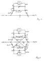
- 1 and 2 show a state variable filter of first and second order, respectively, in which the procedure was carried out by means of evaluation changes according to subclaims 5 and 6, respectively.
- Fig. 1 is a first-order state variable filter with the input signal u (n), with the output signal y (n), with a first summer S1, with a final summer S, through which the input signal weighted d and the status signal x weighted c (n) of the delay element can be combined to form the output signal, as well as recognizable with a distribution node VK1.
- the second input signal of summer S1 must also be amplified by 2 ⁇ . To compensate, the output signal of summer S1 is reduced again by 2 ⁇ .
- a value y is subtracted from a in such a way that it is moved by ⁇ steps to the left by the subsequent sparing, whereby the significant bits are shifted to more significant places as in the spelling of the coefficient b , a shortening of the fixed-point word length is achieved.
- the state signal of the delay element V is thus evaluated with (a- ⁇ ) ⁇ 2 ⁇ and fed back to the input of the same via the summer S 1.
- the status signal x (n) of the delay element V is additionally evaluated with y and fed back directly to the input of the delay element via a further summer S1 '.
- FIG. 2 shows a second-order state variable filter, which in principle represents the doubled, symmetrical representation of the structure according to FIG. 1, the diagonal elements a12 and a21 of the state transition matrix A being added. Since these diagonal elements also have small values, they are shifted to the left by ⁇ or v steps in the same way as the two components b1 and b2 of the first evaluating vector b, which results in the effect described in the description of FIG. 1 .
- FIG. 1 and FIG. 2 require a further multiplier for y or y and 8.
Landscapes
- Physics & Mathematics (AREA)
- Engineering & Computer Science (AREA)
- Computer Hardware Design (AREA)
- Mathematical Physics (AREA)
- Filters That Use Time-Delay Elements (AREA)
- Networks Using Active Elements (AREA)
- Complex Calculations (AREA)
Description
- Die Erfindung bezieht sich auf eine Schaltungsanordnung zur digitalen Filterung eines Eingangssignals gemäss Oberbegriff der Patentansprüche 1 oder 2 (Zustandsvariablenfilter N. Ordnung).
- Zustandsvariablenfilter zweiter Ordnung sind beschrieben in dem Aufsatz von Jackson «Optimal Synthesis of Second-Order State-Space Structures for Digital Filters» in IEEE Transactions on Circuits and Systems, Vol. CAS-26, Nr. 3, März 1979, Seiten 149 bis 153, sowie Zustandsvariablenfilter erster und zweiter Ordnung in dem Aufsatz von Barnes «Roundoff Noise and Overflow in Normal Digital Filters» in IEEE Transactions on Circuits and Systems, Vol. CAS-26, Nr. 3, März 1979, Seiten 154 bis 159.
- Solche Filter werden vornehmlich für schmalbandige Anwendungen realisiert, sie weisen ein geringes Eigenrauschen auf und sind Antwort- und Überlaufstabil. Bei schmalbandigen Filtern rücken die Pole nahe an z = ± 1 in der Ebene der komplexen Frequenz. Das bedeutet, dass bei einem Zustandsvariablenfilter zweiter Ordnung die Komponenten b1 und b2 eines ersten bewertenden Vektors b sowie die Diagonal-Elemente a 12 und a21 der Zustandsübergangsmatrix A sehr kleine Werte gegenüber 1 annehmen und dass die rückkoppelnden Elemente a1 und a22 der Zustandsübergangsmatrix A nahezu den Wert 1 annehmen. Das bedeutet aber, dass bei Festkommaarithmetik eine grosse Koeffizienten-Wortlänge bei der digitalen Realisierung erforderlich ist.
- Aufgabe der vorliegenden Erfindung war es deshalb, eine Schaltungsanordnung für eine Realisierung vorgenannter Zustandsvariablenfilter anzugeben, die es erlaubt, die Koeffizienten-Wortlänge bei Festkommaarithmetik bei gleichbleibender Frequenzganggenauigkeit zu vermindern oder eine Verbesserung der Frequenzganggenauigkeit bei gleichbleibender Koeffizienten-Wortlänge zu erreichen.
- Die Lösung erfolgt mit den kennzeichnenden Merkmalen der beiden Hauptansprüche.
- Die Zustandsvariablenstruktur gemäss vorliegender Erfindung weist die Vorteile auf, dass die Koeffizienten-Wortlänge bei Festkommaarithmetik bei vorgegebener Frequenzganggenauigkeit vermindert wird und/oder, dass die Frequenzganggenauigkeit bei vorgegebener Koeffizienten-Wortlänge verbessert wird. Eine Verminderung der Koeffizienten-Wortlänge führt zu einer Hardware-Realisierung mit kleinerer Speicherplatzaufwendung.
- Durch die Unteransprüche ergeben sich optimale Ausgestaltungen der Erfindung.
- Es folgt nun die Beschreibung der Erfindung anhand der Figuren. Die Fig. 1 und 2 zeigen ein Zustandsvariablenfilter erster bzw. zweiter Ordnung, bei denen mittels Bewertungsänderungen gemäss der Unteransprüche 5 bzw. 6 vorgegangen wurde.
- In Fig. 1 ist ein Zustandsvariablenfilter erster Ordnung mit dem Eingangssignal u(n), mit dem Ausgangssignal y(n), mit einem ersten Summierer S1, mit einem Endsummierer S, durch den das mit d bewertete Eingangssignal und das mit c bewertete Zustandssignal x(n) des Verzögerungsgliedes zum Ausgangssignal zusammengefasst werden, sowie mit einem Verteilerknoten VK1 erkennbar. Erfindungsgemäss wird der erste bewertende Vektor b, der wie eingangs erwähnt, sehr klein gegen 1 ist, um µ Schritte nach links geschiftet, d.h. um den Faktor a = 2µ vergrössert. Entsprechend muss das zweite Eingangssignal des Summierers S1 ebenfalls um 2µ verstärkt werden. Zur Kompensation wird das Ausgangssignal des Summierers S1 um 2-µ wieder verkleinert. Da das Zustandsübergangselement a, wie eingangs erwähnt, nahe 1 ist, wird von a ein Wert y abgezogen derart, dass durch die anschliessende Schiftung um µ Schritte nach links, wodurch die signifikanten Bits wie bei der Schiftung des Koeffizienten b jeweils zu höherwertigen Stellen geschoben werden, eine Verkürzung der Festkomma-Wortlänge erreicht wird. Das Zustandssignal des Verzögerungsgliedes V wird also mit (a-γ) · 2µ bewertet und über den Summierer S 1 dem Eingang desselben wieder zurückgeführt. Als Ausgleichsmassnahme wird das Zustandssignal x(n) des Verzögerungsgliedes V zusätzlich mit y bewertet und über einen weiteren Summierer S1' direkt auf den Eingang des Verzögerungsgliedes zurückgekoppelt. Durch geeignete Wahl des Wertes y kann erreicht werden, dass b und a-y Werte der gleichen Grössenordnung erreichen, d.h. jeweils die gleiche Anzahl führender Nullen der Binärdarstellung aufweisen.
- Die Fig. 2 zeigt ein Zustandsvariablenfilter zweiter Ordnung, das im Prinzip die verdoppelte, symmetrische Darstellung der Struktur nach Fig. 1 darstellt, wobei die Diagonal-Elemente a12 und a21 der Zustandsübergangsmatrix A hinzukommen. Da diese Diagonal-Elemente ebenfalls kleine Werte aufweisen, werden sie in gleicher Weise wie die beiden Komponenten b1 und b2 des ersten bewertenden Vektors b um µ bzw. v Schritte nach links geschiftet, wodurch sich die bei der Beschreibung der Fig. 1 geschilderte Wirkung ergibt. Der einzige Unterschied zwischen den beiden Figuren besteht darin, dass die Kompensationsmassnahme des Rechtsschiftens also die Verkleinerung um a = 2'µ bzw. a = 2-v, nicht direkt am Ausgang der ersten Summierer S 1 bzw. S2 erfolgt, sondern beim Zustandssignal x1 (n) bzw. x2(n) der beiden Verzögerungsglieder V und V2, also am Eingang des Verteilerknotens VK1 bzw. VK2. Dadurch ist die Einsparung der beiden weiteren Summierer S1' bzw. S2' möglich, wenn die genannten Ausgangssignale mit y bzw. 8 bewertet, direkt in die beiden ersten Summierer S1 bzw. S2 geführt werden.
- Eine weitere Verminderung des Filtereigenrauschens ergibt sich, wenn die Wortlänge der Verzögerungsglieder V1 und V2 jeweils um µ bzw. v Überlaufbits vergrössert wird.
- Die Strukturen nach Fig. 1 bzw. Fig. 2 machen einen weiteren Multiplizierer für y bzw. y und 8 erforderlich.
- Dies kann verhindert werden durch eine geeignete Wahl von y und 8. Erstens kann y = 8 = 1 gewählt werden, so dass der Multiplizierer für die Bewertung mit y bzw. 8 entfallen kann. Zweitens kann y und 8 so bemessen werden, dass y = a11 ± 2-µ und entsprechend 8 = a22 ± 2-v bemessen wird, wodurch (a11 -γ) · 2µ = ± 1 und (a22-δ) 2v _ ± 1 werden, wodurch die entsprechende Bewertung mittels eines Multiplizierers entfallen kann für eine direkte Durchreichung des Signals oder erforderlichenfalls unter Zwischenschaltung eines Inverters, welcher jedoch weniger aufwendig ist als ein Multiplizierer.
- Es wurde aufgezeigt, dass mit Hilfe der erfindungsgemässen Zustandsvariablenstruktur eine Verminderung der Festkomma-Koeffizienten-Wortlänge bei vorgegebener Frequenzganggenauigkeit und/oder eine Verbesserung der Frequenzganggenauigkeit bei vorgegebener Koeffizienten-Wortlänge erreicht wird, wodurch insgesamt ein geringerer Hardware-Realisierungsaufwand notwendig ist.
Claims (8)
Priority Applications (4)
| Application Number | Priority Date | Filing Date | Title |
|---|---|---|---|
| AT83109680T ATE28015T1 (de) | 1983-09-28 | 1983-09-28 | Zustandsvariablenfilter. |
| DE8383109680T DE3372243D1 (en) | 1983-09-28 | 1983-09-28 | State-variable filter |
| EP83109680A EP0135606B1 (de) | 1983-09-28 | 1983-09-28 | Zustandsvariablenfilter |
| JP59200718A JPS6091712A (ja) | 1983-09-28 | 1984-09-27 | N次状態変数フイルタ |
Applications Claiming Priority (1)
| Application Number | Priority Date | Filing Date | Title |
|---|---|---|---|
| EP83109680A EP0135606B1 (de) | 1983-09-28 | 1983-09-28 | Zustandsvariablenfilter |
Publications (2)
| Publication Number | Publication Date |
|---|---|
| EP0135606A1 EP0135606A1 (de) | 1985-04-03 |
| EP0135606B1 true EP0135606B1 (de) | 1987-06-24 |
Family
ID=8190707
Family Applications (1)
| Application Number | Title | Priority Date | Filing Date |
|---|---|---|---|
| EP83109680A Expired EP0135606B1 (de) | 1983-09-28 | 1983-09-28 | Zustandsvariablenfilter |
Country Status (4)
| Country | Link |
|---|---|
| EP (1) | EP0135606B1 (de) |
| JP (1) | JPS6091712A (de) |
| AT (1) | ATE28015T1 (de) |
| DE (1) | DE3372243D1 (de) |
Families Citing this family (4)
| Publication number | Priority date | Publication date | Assignee | Title |
|---|---|---|---|---|
| JPS61244937A (ja) * | 1985-04-24 | 1986-10-31 | Yaskawa Electric Mfg Co Ltd | 電気機械における機械系の固有振動抑制方式 |
| DE3522412A1 (de) * | 1985-06-22 | 1987-01-02 | Ant Nachrichtentech | Digitales rekursiv-filter |
| DE3522411A1 (de) * | 1985-06-22 | 1987-01-02 | Ant Nachrichtentech | Digitales rekursiv-filter |
| JPS6228544A (ja) * | 1985-07-31 | 1987-02-06 | Yaskawa Electric Mfg Co Ltd | 電気機械における機械系の固有振動抑制方式 |
-
1983
- 1983-09-28 DE DE8383109680T patent/DE3372243D1/de not_active Expired
- 1983-09-28 AT AT83109680T patent/ATE28015T1/de not_active IP Right Cessation
- 1983-09-28 EP EP83109680A patent/EP0135606B1/de not_active Expired
-
1984
- 1984-09-27 JP JP59200718A patent/JPS6091712A/ja active Pending
Also Published As
| Publication number | Publication date |
|---|---|
| ATE28015T1 (de) | 1987-07-15 |
| EP0135606A1 (de) | 1985-04-03 |
| JPS6091712A (ja) | 1985-05-23 |
| DE3372243D1 (en) | 1987-07-30 |
Similar Documents
| Publication | Publication Date | Title |
|---|---|---|
| DE69306753T2 (de) | Verstärker mit programmierbaren Verstärkungsfaktor | |
| DE69107059T2 (de) | Sigma-delta-modulator. | |
| DE102009039428B4 (de) | Digitalfilter | |
| DE69817270T2 (de) | Anordnung zur Erzeugung von analogen Signalen unter Benutzung von Analog-Digitalwandlern, besonders für direkte digitale Synthese | |
| DE19729650A1 (de) | Einrichtung zur Phasen- und/oder Frequenzregelung | |
| DE69422650T2 (de) | Als dreistufiges transversales Filter anwendbare digitale Filterschaltung | |
| EP1138120B1 (de) | Analog-digital-umsetzer | |
| EP0461282B1 (de) | Überabtastender Analog-Digital-Umsetzer mit Rauschfilterung in Switched-Capacitor-Technik | |
| DE4320691C2 (de) | D/A-Wandler | |
| DE602005001311T2 (de) | Schaltverstärker | |
| EP0135606A1 (de) | Zustandsvariablenfilter | |
| DE3751088T2 (de) | Signalverarbeitungseinrichtung. | |
| DE2612764C2 (de) | Spannungs-Frequenz-Wandler | |
| DE102005018858A1 (de) | Digitales Filter und Verfahren zur Bestimmung seiner Koeffizienten | |
| DE2816831B2 (de) | Variabler Entzerrer | |
| DE3688039T2 (de) | Digital/analog-umwandler. | |
| DE69901037T2 (de) | Verzögerungskompensation des a/d wandlers in sigma-delta modulatoren | |
| EP1290791A1 (de) | Digitales interpolationsfilter | |
| DE19701067B4 (de) | Verfahren und Schaltungsanordnung zur Frequenzvervielfachung | |
| EP0205836B1 (de) | Digitales Rekursiv-Filter | |
| EP0532781B1 (de) | Integrierte Schaltungsanordnung mit einem analogen Netzwerk | |
| DE19640072A1 (de) | Nach dem Prinzip der fraktionalen Frequenzsynthese arbeitender Frequenzsynthesizer | |
| EP1203451B1 (de) | Frequenzsynthesizer | |
| EP0367932B1 (de) | Filterbank zum Frequenzmultiplexen bzw. Frequenzmultiplexen von Kanalsignalen | |
| DE3302550C2 (de) |
Legal Events
| Date | Code | Title | Description |
|---|---|---|---|
| PUAI | Public reference made under article 153(3) epc to a published international application that has entered the european phase |
Free format text: ORIGINAL CODE: 0009012 |
|
| AK | Designated contracting states |
Designated state(s): AT CH DE FR GB LI |
|
| 17P | Request for examination filed |
Effective date: 19850910 |
|
| 17Q | First examination report despatched |
Effective date: 19860902 |
|
| GRAA | (expected) grant |
Free format text: ORIGINAL CODE: 0009210 |
|
| AK | Designated contracting states |
Kind code of ref document: B1 Designated state(s): AT CH DE FR GB LI |
|
| REF | Corresponds to: |
Ref document number: 28015 Country of ref document: AT Date of ref document: 19870715 Kind code of ref document: T |
|
| ET | Fr: translation filed | ||
| REF | Corresponds to: |
Ref document number: 3372243 Country of ref document: DE Date of ref document: 19870730 |
|
| PLBE | No opposition filed within time limit |
Free format text: ORIGINAL CODE: 0009261 |
|
| STAA | Information on the status of an ep patent application or granted ep patent |
Free format text: STATUS: NO OPPOSITION FILED WITHIN TIME LIMIT |
|
| 26N | No opposition filed | ||
| PGFP | Annual fee paid to national office [announced via postgrant information from national office to epo] |
Ref country code: GB Payment date: 19930913 Year of fee payment: 11 |
|
| PGFP | Annual fee paid to national office [announced via postgrant information from national office to epo] |
Ref country code: FR Payment date: 19930916 Year of fee payment: 11 |
|
| PGFP | Annual fee paid to national office [announced via postgrant information from national office to epo] |
Ref country code: AT Payment date: 19930924 Year of fee payment: 11 |
|
| PGFP | Annual fee paid to national office [announced via postgrant information from national office to epo] |
Ref country code: CH Payment date: 19931021 Year of fee payment: 11 |
|
| PG25 | Lapsed in a contracting state [announced via postgrant information from national office to epo] |
Ref country code: GB Effective date: 19940928 Ref country code: AT Effective date: 19940928 |
|
| PG25 | Lapsed in a contracting state [announced via postgrant information from national office to epo] |
Ref country code: LI Effective date: 19940930 Ref country code: CH Effective date: 19940930 |
|
| GBPC | Gb: european patent ceased through non-payment of renewal fee |
Effective date: 19940928 |
|
| PG25 | Lapsed in a contracting state [announced via postgrant information from national office to epo] |
Ref country code: FR Effective date: 19950531 |
|
| REG | Reference to a national code |
Ref country code: CH Ref legal event code: PL |
|
| REG | Reference to a national code |
Ref country code: FR Ref legal event code: ST |
|
| PGFP | Annual fee paid to national office [announced via postgrant information from national office to epo] |
Ref country code: DE Payment date: 19960523 Year of fee payment: 13 |
|
| PG25 | Lapsed in a contracting state [announced via postgrant information from national office to epo] |
Ref country code: DE Effective date: 19970603 |