EP0135688A2 - Procédé de fabrication d'une lampe électroluminescente - Google Patents
Procédé de fabrication d'une lampe électroluminescente Download PDFInfo
- Publication number
- EP0135688A2 EP0135688A2 EP84107894A EP84107894A EP0135688A2 EP 0135688 A2 EP0135688 A2 EP 0135688A2 EP 84107894 A EP84107894 A EP 84107894A EP 84107894 A EP84107894 A EP 84107894A EP 0135688 A2 EP0135688 A2 EP 0135688A2
- Authority
- EP
- European Patent Office
- Prior art keywords
- conductive
- coating
- carrier strip
- conductive layer
- conductive material
- Prior art date
- Legal status (The legal status is an assumption and is not a legal conclusion. Google has not performed a legal analysis and makes no representation as to the accuracy of the status listed.)
- Withdrawn
Links
Images

Classifications
-
- H—ELECTRICITY
- H05—ELECTRIC TECHNIQUES NOT OTHERWISE PROVIDED FOR
- H05B—ELECTRIC HEATING; ELECTRIC LIGHT SOURCES NOT OTHERWISE PROVIDED FOR; CIRCUIT ARRANGEMENTS FOR ELECTRIC LIGHT SOURCES, IN GENERAL
- H05B33/00—Electroluminescent light sources
- H05B33/10—Apparatus or processes specially adapted to the manufacture of electroluminescent light sources
Definitions
- This invention relates to the process for manufacturing thin flexible electroluminescent lamps in a continuous operation. More particularly, it relates to continuous manufacture of flexible electroluminescent lamps of a type in which exposed conductive areas for two or more electrodes are formed from the same layer of conductive material as part of the operation.
- Electroluminescent displays were allegedly first discovered by Destriau in Paris in 1936. However, the first practical applications commenced around 1949.
- An early type of flexible electroluminescent lamp comprised a laminated structure enclosed in outer thermoplastic sheets forming an envelope and laminated with a vacuum plate.
- the active components of the electroluminescent lamp comprised an aluminum foil, a layer of insulation with a high dielectric constant overcoated with a layer of electroluminescent phosphor and finally overlayed with a sheet of conducting glass paper.
- two leads to activate the lamp were pressed against the aluminum foil and the conductive glass paper respectively and were embedded as part of the laminated structure. The leads extended out through the thermoplastic envelope.
- Such a construction is described in U.S. Patent 3,047,052 - Friedrich.
- U.S. Patent 3,252,845 discloses a flexible electroluminescent lamp, in which, rather than depositing the phosphor on an imperforate sheet of foil, employs a temporary support member and deposits the electroluminescent phosphor, dispersed in an organic polymeric matrix on a transparent conductive glass paper. Next, a thin insulating layer having a high dielectric constant, likewise dispersed in an organic polymeric matrix, is applied; and lastly, a back electrode of electrically conductive paint or paste or similar material is brushed, rolled, sprayed, or silk screened onto the insulating layer. The terminals are attached and the entire member enclosed between thermoplastic material and laminated in a hydrostatic press.
- U.S. Patent 4,066,925 - Dickson Another approach to providing continuous manufacture of flexible electroluminescent lamps is shown in U.S. Patent 4,066,925 - Dickson.
- Two preform webs are pressed together to provide large area electroluminescent devices.
- the preforms are manufactured ahead of time and stored in rolls.
- One preform comprises a conductive metal foil with a dispersion of electroluminescent particles in a polymeric binder.
- the other preform is a transparent substrate with a three-layer transparent electrode deposited thereon.
- electroluminescent lamps have the electric driving signals applied to transversely spaced parallel conductive plates on opposite flexible split-electrode electroluminescent lamp comprising the steps of providing a transparent flexible carrier strip of insulating plastic material with a first continuous transparent coating of conductive material on it, continuously moving the carrier strip while depositing a slurry of a mixture of uncured epoxy resin and electroluminescent phosphor, passing the carrier strip through a curing oven and curing the resin to bond the phosphor material in a flexible matrix and to cause it to adhere to the first coating, depositing a slurry of liquid-borne conductive particulate matter continuously on the carrier strip, drying the slurry to provide a second continuous coating of electrically conductive material, removing conductive material to define a narrow groove in one of the conductive coatings, thereby providing at least two contiguous laterally spaced electrodes formed from the same conductive layer, and cutting the carrier strip into a desired lamp size.
- the narrow groove is formed in the second conductive coating, but in a modified
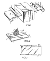
- Figures 1-5 The preferred form of process is shown in Figures 1-5.
- a continuous carrier strip 1 of transparent insulating material which is conveniently stored on a roll 2.
- Means are provided to uncoil the carrier strip and drive it through a series of take-up rolls and guiding devices (not shown) and ultimately to coil the strip on another roll 3 at the other end of the line.
- a conventional motor drive (not shown) continuously moves the carrier strip 1 at a substantially continuous speed which may be selected in the range of sides of the phosphor.
- a "split electrode" construction for an electroluminescent lamp is disclosed in U.S. Patent 2,928,974 issued March 15, 1960 to D.H. Mash.
- the split electrode construction attaches the source of electric driving voltage to laterally spaced electrodes, i.e. electrodes from the same conductive layer separated by a narrow insulating gap while the other transversely spaced conductive layer serves as a "floating" member and capacitively couples the two driving electrodes.
- the back electrode of lead dioxide was divided by scratching or cutting through the coating along a rectangular zig-zag line.
- the conductive layer connnected to the driving electrodes can be provided either from an embedded conductive transparent layer (Dickson) or from the conductive back layer, (Mash) which may or may not be opaque.
- the present invention provides a process for conveniently manufacturing a flexible electroluminescent lamp employing the advantages of the split electrode construction.
- one object of the present invention is to provide a process for continuously manufacturing flexible electroluminescent lamps by applying the materials throughout the course of the process on a carrier strip, which itself becomes part of the lamp.
- Another object of the invention is to provide a process for manufacturing a flexible electroluminescent lamp with a split electrode construction for ease of attachment of the connectors to the lamp.
- Still another object of the invention is to provide an improved process for manufacturing flexible electroluminescent lamps for large area displays in a continuous production process.
- the invention comprises the process of making a 10-20 feet per minute.
- the carrier strip of transparent insulating material is preferably Mylar, a registered trademark of E. I. duPont de Nemours and Co., preferably having a thickness of about 5 mils.
- a first continuous thin transparent coating 4 of electrically conductive material is provided on the carrier strip.
- the conductive coating may be indium tin oxide having a thickness of approximately 1000 Angstroms.
- Mylar with such a transparent conductive coating is commercially available as a material called Intrex, a registered trademark of the Sierracin Corporation.
- a gravity feed trough 5 serves to deposit a slurry of a mixture of uncured epoxy resin and electroluminescent phosphor particles indicated by reference number 6 on top of the conductive coating 4 to a controlled thickness on the order of 1 to 5 mils, preferably 3.5 mills.
- Various types and particle sizes of phosphors and various types of uncured epoxy resins may be employed.
- a preferred mixture is a GTE Sylvania No. 727 phosphor intermixed with a two-part epoxy which serves as a dielectric binder in the proportion of 4:1 for phosphor and binder respectively.
- One epoxy resin binder which may be used is LOCTITE 75, commercially available from Loctite Corporation.
- a typical controlled layer thickness may be on the order of 3.5 mils.
- Other types of curable resin binder materials may be used which are well-known.
- the epoxy binder is cured while travelling through a curing oven 7 at a temperature of approximately 140°C. This cures the epoxy and binds the electroluminescent phosphor material throughout the resin in a dielectric matrix and causes it to adhere to the conductive layer 4.
- the cured electroluminescent matrix layer, shown at 8 as it leaves the curing oven, is still relatively flexible.
- Other known means of curing the resin binder such as ultraviolet radiation may be used.
- a slurry of liquid-borne conductive particulate matter is deposited continuously on the carrier strip.
- the slurry may be sprayed from spray nozzles 9, and is preferably a water-borne, air-drying, nickel-filled, acrylic coating which is commercially available as EMILUX, a trademark of General Electric Company.
- the liquid carrier is driven off by means such as infrared heating lamps 10 to leave a dried second continuous coating of electrically conductive material, shown at 11, on top of the coating 8, having a thickness of approximately 2 mils.
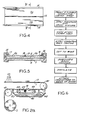
- the conductive material is removed from the conductive layer 11, as illustrated in Fig. 2. This step may be carried out while the strip is continuously moving in a subsequent stage (not shown), as in Fig. 1, or it may be performed while, or after, the strip has been severed to a selected lamp size, as shown in Fig. 2.
- Conductive material is removed from the conductive layer 11 to define a narrow groove 13 in the conductive coating, thereby providing at least two laterally spaced contiguous electrodes, lla and llb, as shown in Fig. 2.
- One removal technique is to apply a solvent to the second conductive coating 11, protect the coating by means of a shield 12, and then to brush away the conductive material with brush 19.
- conductive coating 11 to provide a narrow groove is only shown in very simplified form in Fig. 2.
- the preferred process extends the length of the carrier strip in Fig. 1 beyond the drying lamps, as illustrated in Fig. 2a, by means of idler rollers 40, 41.
- the rollers extend the path of the carrier strip and invert it so that the conductive layer 11 is on the bottom of the laminated strip.
- a liquid solvent such as 81ankothan& is sprayed from a jet 42 on the conductive layer 11 in the area to be removed.
- the shields on either side of the area to be removed are shown as a pair of continuous belts 43 mounted on tapered rollers 44, 45 so that the belts 43 are spread apart and move at the same speed as the carrier strip.
- the brush 19 removes the conductive coating in the space between belts 43.
- the solvent and waste material is collected in a pan 46 beneath the belt and filtered for recirculation.
- Air jets 47 dry the coating and evaporate the solvent on the carrier strip, the strip is rolled up at 3 and stored for the subsequent severing and assembly operations.
- Another technique (not shown) is to employ a precision saw blade removing the conductive layer 11 down to the dielectric matrix 8. This may be done either as part of a continuous slitting and cut off operation, or in a subsequent operation as depicted to provide a groove 13 separating the electrodes lla and 11b.
- Fig. 3-5 Insulating plastic connector holders 14, 15 are attached to opposite sides of the coated sheet.
- Fig. 3 shows the front side of the lamp and Fig. 4 the rear side.
- the groove 13 is then preferably filled with a high dielectric strength insulating material 16.
- the two exposed areas on lla and llb are contacted by electrically conductive pads 17, 18 which may be either conductive rubber or mechanical spring pads.
- electrically conductive pads 17, 18 may be either conductive rubber or mechanical spring pads.
- many types of connectors may be employed and adapted to contact the exposed areas of the lamp electrodes.
- a flow chart of the process steps is shown in Fig. 6.
- Figs. 7-11 illustrate a modified form of the process.
- the carrier strip 20 of transparent insulating material, coated with transparent conductive coating 21 is fed through a series of steps and wound onto a take-up roll 22 in the same manner as before.
- the conductive material is removed from the initial conductive coating 21 to provide two contiguous laterally spaced electrode sections 21a, 21b with a narrow groove 23 between them.
- the conductive indium oxide may be continuously removed by an electric arc established between an electrode 24 and the grounded conductive coating.
- a power supply 25 supplies a potential of 60 volts DC, which effectively removes the onductive coating, leaving a gap of approximately .127 millimeters.
- the epoxy/phosphor mixture 26 is applied from gravity feed trough 27.
- Moveable end walls 28 allow the width of the layer 29 to be adjusted, so as to leave the conductive layer 21 exposed on opposite sides of the carrier strip, for reasons to be explained.
- the epoxy binder is cured as before while travelling through curing oven 30.
- a second feed trough 31 feeds the liquid borne slurry of conductive material 32, such as Emilux, and the infrared lamp 33 drives off the liquid leaving a layer 34 approximately 2 mils thick, which is substantially opaque.
- the flexible sheet material is cut into desired lengths 35 and flexible connector holders 36 are attached to opposite sides of the sheet.
- Terminals 37 provide for making external connections to the power supply.
- the connector holders 36 may also be flexible, as indicated at 38, so that the lamp may be fitted to a contour.
- Fig. 10 shows that the connectors 36 may be arranged to clamp together over the opposite side edges of the sheet.
- a conductive pad 39 makes electrical contact with the exposed areas of conductive electrodes 21a, 21b at the edges of the strip.
- the pad 39 may be a mechanical spring member of conductive metal also.
- the contiguous electrodes are formed from the first conductive layer or from the second conductive layer, attachment of a source of drive voltage to the electrodes will cause the opposite laterally electrode to capacitively couple the AC driving voltage through the dielectric matrix by way of the opposite "floating electrode” and cause the phosphor to luminesce. This will be visible through the transparent carrier strip member, which becomes a part of the lamp upon completion of the process.
- the overall lamp will be approximately 10 mils in thickness having great flexibility and in no case thicker than approximately 15 mils.
Landscapes
- Engineering & Computer Science (AREA)
- Manufacturing & Machinery (AREA)
- Electroluminescent Light Sources (AREA)
Applications Claiming Priority (2)
| Application Number | Priority Date | Filing Date | Title |
|---|---|---|---|
| US528310 | 1983-08-31 | ||
| US06/528,310 US4534743A (en) | 1983-08-31 | 1983-08-31 | Process for making an electroluminescent lamp |
Publications (2)
| Publication Number | Publication Date |
|---|---|
| EP0135688A2 true EP0135688A2 (fr) | 1985-04-03 |
| EP0135688A3 EP0135688A3 (fr) | 1986-02-19 |
Family
ID=24105144
Family Applications (1)
| Application Number | Title | Priority Date | Filing Date |
|---|---|---|---|
| EP84107894A Withdrawn EP0135688A3 (fr) | 1983-08-31 | 1984-07-06 | Procédé de fabrication d'une lampe électroluminescente |
Country Status (2)
| Country | Link |
|---|---|
| US (1) | US4534743A (fr) |
| EP (1) | EP0135688A3 (fr) |
Cited By (5)
| Publication number | Priority date | Publication date | Assignee | Title |
|---|---|---|---|---|
| WO2000027169A1 (fr) * | 1998-10-30 | 2000-05-11 | Minnesota Mining And Manufacturing Company | Dispositif electroluminescent, et procede de production correspondant |
| US6479941B1 (en) | 1998-10-30 | 2002-11-12 | 3M Innovative Properties Company | Electroluminescent device and method for the production of the same |
| DE102006045294A1 (de) * | 2006-09-26 | 2008-03-27 | Siemens Ag | Verfahren zum Herstellen einer organischen Leuchtdiode und organische Leuchtdiode |
| KR101272652B1 (ko) * | 2008-07-15 | 2013-06-11 | 오픈마인드 테크놀로지스 아게 | 밀링공구를 이용하여 비 가공 재료로부터 가공된 완성품을 제조하는 방법 |
| WO2014070442A1 (fr) * | 2012-10-30 | 2014-05-08 | Sonoco Development Incorporated | Dispositif d'affichage électroluminescent et procédé de fabrication |
Families Citing this family (34)
| Publication number | Priority date | Publication date | Assignee | Title |
|---|---|---|---|---|
| US4684353A (en) * | 1985-08-19 | 1987-08-04 | Dunmore Corporation | Flexible electroluminescent film laminate |
| US5045755A (en) * | 1987-05-27 | 1991-09-03 | E-Lite Technologies, Inc. | Electroluminescent panel lamp with integral electrical connector |
| AU2269692A (en) * | 1991-06-24 | 1993-01-25 | Durel Corporation | Electroluminescent lamp |
| US5276382A (en) * | 1991-08-20 | 1994-01-04 | Durel Corporation | Lead attachment for electroluminescent lamp |
| US5946431A (en) * | 1993-07-30 | 1999-08-31 | Molecular Dynamics | Multi-functional photometer with movable linkage for routing light-transmitting paths using reflective surfaces |
| US5491379A (en) * | 1994-10-11 | 1996-02-13 | Timex Corporation | Electroluminescent edge connect-composite lamp/strip and method of making the same |
| US5720639A (en) * | 1995-06-07 | 1998-02-24 | American International Pacific Industries, Corp. | Method for manufacturing electroluminescent lamp systems |
| JPH11510948A (ja) * | 1995-08-11 | 1999-09-21 | ミネソタ マイニング アンド マニュファクチャリング カンパニー | 多層光学フィルムを用いたエレクトロルミネッセンスランプ |
| US5757125A (en) * | 1995-11-09 | 1998-05-26 | Astronics Corporation, Inc. | Electroluminescent lamp with lead attachment isolation structure, and rotary abrasion method of manufacture thereof |
| JP2000504469A (ja) * | 1996-02-22 | 2000-04-11 | アメリカン インターナショナル パシフィック インダストリーズ コープ. | 放電発光ランプの製造方法 |
| US6054809A (en) * | 1996-08-14 | 2000-04-25 | Add-Vision, Inc. | Electroluminescent lamp designs |
| US5947584A (en) * | 1997-03-19 | 1999-09-07 | Passanante; Caesar A. | Illuminated trash receptacle |
| US6066830A (en) * | 1998-06-04 | 2000-05-23 | Astronics Corporation | Laser etching of electroluminescent lamp electrode structures, and electroluminescent lamps produced thereby |
| US7288014B1 (en) | 2000-10-27 | 2007-10-30 | Science Applications International Corporation | Design, fabrication, testing, and conditioning of micro-components for use in a light-emitting panel |
| US6935913B2 (en) * | 2000-10-27 | 2005-08-30 | Science Applications International Corporation | Method for on-line testing of a light emitting panel |
| US6764367B2 (en) * | 2000-10-27 | 2004-07-20 | Science Applications International Corporation | Liquid manufacturing processes for panel layer fabrication |
| US6545422B1 (en) | 2000-10-27 | 2003-04-08 | Science Applications International Corporation | Socket for use with a micro-component in a light-emitting panel |
| US6822626B2 (en) | 2000-10-27 | 2004-11-23 | Science Applications International Corporation | Design, fabrication, testing, and conditioning of micro-components for use in a light-emitting panel |
| US6612889B1 (en) | 2000-10-27 | 2003-09-02 | Science Applications International Corporation | Method for making a light-emitting panel |
| US6570335B1 (en) | 2000-10-27 | 2003-05-27 | Science Applications International Corporation | Method and system for energizing a micro-component in a light-emitting panel |
| US6801001B2 (en) | 2000-10-27 | 2004-10-05 | Science Applications International Corporation | Method and apparatus for addressing micro-components in a plasma display panel |
| US6796867B2 (en) * | 2000-10-27 | 2004-09-28 | Science Applications International Corporation | Use of printing and other technology for micro-component placement |
| US6620012B1 (en) | 2000-10-27 | 2003-09-16 | Science Applications International Corporation | Method for testing a light-emitting panel and the components therein |
| US6762566B1 (en) | 2000-10-27 | 2004-07-13 | Science Applications International Corporation | Micro-component for use in a light-emitting panel |
| US6989412B2 (en) * | 2001-06-06 | 2006-01-24 | Henkel Corporation | Epoxy molding compounds containing phosphor and process for preparing such compositions |
| US6833669B2 (en) * | 2001-06-25 | 2004-12-21 | E-Lite Technologies, Inc. | Method and apparatus for making large-scale laminated foil-back electroluminescent lamp material, as well as the electroluminescent lamps and strip lamps produced therefrom |
| US6607413B2 (en) * | 2001-06-29 | 2003-08-19 | Novatech Electro-Luminescent, Inc. | Method for manufacturing an electroluminescent lamp |
| US6896388B2 (en) * | 2002-04-03 | 2005-05-24 | E-Lite Technologies, Inc. | Path marking and lighting system |
| JP2004342336A (ja) | 2003-05-13 | 2004-12-02 | Semiconductor Energy Lab Co Ltd | 発光装置およびその作製方法 |
| US7192326B2 (en) * | 2003-08-29 | 2007-03-20 | Semiconductor Energy Laboratory Co., Ltd. | Method of manufacturing a light-emitting element using a rubbing treatment |
| US20050124258A1 (en) * | 2003-12-08 | 2005-06-09 | E-Lite Technologies, Inc. | Electroluminescent lamp construction and electroluminescent lamp made thereby |
| US7204050B2 (en) * | 2003-12-29 | 2007-04-17 | Sargent Manufacturing Company | Exit device with lighted touchpad |
| US20050189164A1 (en) * | 2004-02-26 | 2005-09-01 | Chang Chi L. | Speaker enclosure having outer flared tube |
| EP2227512A1 (fr) | 2007-12-18 | 2010-09-15 | Lumimove, Inc., Dba Crosslink | Dispositifs et systèmes électroluminescents flexibles |
Family Cites Families (6)
| Publication number | Priority date | Publication date | Assignee | Title |
|---|---|---|---|---|
| US2928974A (en) * | 1954-07-02 | 1960-03-15 | Thorn Electrical Ind Ltd | Electro-luminescent device |
| US3047052A (en) * | 1958-07-14 | 1962-07-31 | Gen Electric | Apparatus for laminating an electroluminescent cell lay-up |
| US3519871A (en) * | 1966-02-05 | 1970-07-07 | Mitsubishi Plastics Ind | Electroluminescent cell of novel structure |
| US3895208A (en) * | 1973-09-28 | 1975-07-15 | Siemens Ag | Method and device for the production of metal-free paths on metalized insulator foils |
| FR2457148A1 (fr) * | 1979-05-25 | 1980-12-19 | Electricite De France | Procede et dispositif d'elimination locale de revetement metallique |
| US4417174A (en) * | 1980-10-03 | 1983-11-22 | Alps Electric Co., Ltd. | Electroluminescent cell and method of producing the same |
-
1983
- 1983-08-31 US US06/528,310 patent/US4534743A/en not_active Expired - Fee Related
-
1984
- 1984-07-06 EP EP84107894A patent/EP0135688A3/fr not_active Withdrawn
Cited By (6)
| Publication number | Priority date | Publication date | Assignee | Title |
|---|---|---|---|---|
| WO2000027169A1 (fr) * | 1998-10-30 | 2000-05-11 | Minnesota Mining And Manufacturing Company | Dispositif electroluminescent, et procede de production correspondant |
| AU750438B2 (en) * | 1998-10-30 | 2002-07-18 | Minnesota Mining And Manufacturing Company | Electroluminescent device and method for the production of the same |
| US6479941B1 (en) | 1998-10-30 | 2002-11-12 | 3M Innovative Properties Company | Electroluminescent device and method for the production of the same |
| DE102006045294A1 (de) * | 2006-09-26 | 2008-03-27 | Siemens Ag | Verfahren zum Herstellen einer organischen Leuchtdiode und organische Leuchtdiode |
| KR101272652B1 (ko) * | 2008-07-15 | 2013-06-11 | 오픈마인드 테크놀로지스 아게 | 밀링공구를 이용하여 비 가공 재료로부터 가공된 완성품을 제조하는 방법 |
| WO2014070442A1 (fr) * | 2012-10-30 | 2014-05-08 | Sonoco Development Incorporated | Dispositif d'affichage électroluminescent et procédé de fabrication |
Also Published As
| Publication number | Publication date |
|---|---|
| EP0135688A3 (fr) | 1986-02-19 |
| US4534743A (en) | 1985-08-13 |
Similar Documents
| Publication | Publication Date | Title |
|---|---|---|
| US4534743A (en) | Process for making an electroluminescent lamp | |
| US5045755A (en) | Electroluminescent panel lamp with integral electrical connector | |
| US6833669B2 (en) | Method and apparatus for making large-scale laminated foil-back electroluminescent lamp material, as well as the electroluminescent lamps and strip lamps produced therefrom | |
| US5792298A (en) | Method of making a laminated glass pane with embedded antenna wires | |
| US5830028A (en) | Roll coated EL panel | |
| AU598629B2 (en) | Electroluminescent panel lamp and method for manufacturing | |
| US5488266A (en) | Electro-luminescence device | |
| DE69932337T2 (de) | Herstellungsverfahren einer anzeigetafel unter verwendung eines klebemittelauftragungsverfahren | |
| US2852423A (en) | Shielding adhesive tape | |
| RU2082285C1 (ru) | Способ изготовления электролюминесцентной индикаторной панели и электролюминесцентная индикаторная панель | |
| DE4126533A1 (de) | Verfahren zum kontaktieren von elektrisch heizbaren glasscheiben mit transparenten heizwiderstandsschichten | |
| CN1496783A (zh) | 片层压铝质型材的制造方法和设备 | |
| BR8103421A (pt) | Folha metalica combinanada de eletrodo para capacitor eletrico processo de fabbricacao da folha metalica capacitor eletrico queusa o dito eletro e processo de producao do capacitor do tipo de correcao de fator | |
| US7105998B2 (en) | EL light emitting device with waterproof function | |
| EP0442885B1 (fr) | Procede de production d'une lampe electroluminescente | |
| US3895207A (en) | Method and device for the production of metal-free paths on metalized insulator foils | |
| US20050124258A1 (en) | Electroluminescent lamp construction and electroluminescent lamp made thereby | |
| DE69421584T2 (de) | Elektrische beheizte Verbundglasscheibe | |
| JPS59201392A (ja) | 分散型エレクトロルミネツセンス素子の製造方法 | |
| US3318751A (en) | Apparatus for forming metal-paper laminate electrostatically | |
| DE2431020C2 (de) | Verfahren zur Herstellung regenerierfähiger, elektrischer Schichtkondensatoren | |
| CN101023293A (zh) | 大面积电致发光灯 | |
| DE102004004311A1 (de) | Herstellungsverfahren für eine El-Lampe | |
| KR820001912Y1 (ko) | 정전식 표시장치의 유전체층 | |
| JP2005174849A (ja) | プラズマディスプレイパネルの製造方法 |
Legal Events
| Date | Code | Title | Description |
|---|---|---|---|
| PUAI | Public reference made under article 153(3) epc to a published international application that has entered the european phase |
Free format text: ORIGINAL CODE: 0009012 |
|
| AK | Designated contracting states |
Designated state(s): BE CH DE FR GB LI NL SE |
|
| PUAL | Search report despatched |
Free format text: ORIGINAL CODE: 0009013 |
|
| AK | Designated contracting states |
Designated state(s): BE CH DE FR GB LI NL SE |
|
| STAA | Information on the status of an ep patent application or granted ep patent |
Free format text: STATUS: THE APPLICATION HAS BEEN WITHDRAWN |
|
| 18W | Application withdrawn |
Withdrawal date: 19860827 |
|
| RIN1 | Information on inventor provided before grant (corrected) |
Inventor name: KITIK, WALTER Inventor name: D'ONOFRIO, ANTHONY |