EP0136237B1 - Halterung für Gehäuse für eine integrierte Schaltung - Google Patents
Halterung für Gehäuse für eine integrierte Schaltung Download PDFInfo
- Publication number
- EP0136237B1 EP0136237B1 EP19840401898 EP84401898A EP0136237B1 EP 0136237 B1 EP0136237 B1 EP 0136237B1 EP 19840401898 EP19840401898 EP 19840401898 EP 84401898 A EP84401898 A EP 84401898A EP 0136237 B1 EP0136237 B1 EP 0136237B1
- Authority
- EP
- European Patent Office
- Prior art keywords
- holder
- cover
- power source
- integrated circuit
- pins
- Prior art date
- Legal status (The legal status is an assumption and is not a legal conclusion. Google has not performed a legal analysis and makes no representation as to the accuracy of the status listed.)
- Expired
Links
Images





Classifications
-
- H—ELECTRICITY
- H05—ELECTRIC TECHNIQUES NOT OTHERWISE PROVIDED FOR
- H05K—PRINTED CIRCUITS; CASINGS OR CONSTRUCTIONAL DETAILS OF ELECTRIC APPARATUS; MANUFACTURE OF ASSEMBLAGES OF ELECTRICAL COMPONENTS
- H05K7/00—Constructional details common to different types of electric apparatus
- H05K7/02—Arrangements of circuit components or wiring on supporting structure
- H05K7/10—Plug-in assemblages of components, e.g. IC sockets
- H05K7/1092—Plug-in assemblages of components, e.g. IC sockets with built-in components, e.g. intelligent sockets
-
- H—ELECTRICITY
- H01—ELECTRIC ELEMENTS
- H01M—PROCESSES OR MEANS, e.g. BATTERIES, FOR THE DIRECT CONVERSION OF CHEMICAL ENERGY INTO ELECTRICAL ENERGY
- H01M50/00—Constructional details or processes of manufacture of the non-active parts of electrochemical cells other than fuel cells, e.g. hybrid cells
- H01M50/20—Mountings; Secondary casings or frames; Racks, modules or packs; Suspension devices; Shock absorbers; Transport or carrying devices; Holders
- H01M50/204—Racks, modules or packs for multiple batteries or multiple cells
- H01M50/207—Racks, modules or packs for multiple batteries or multiple cells characterised by their shape
- H01M50/216—Racks, modules or packs for multiple batteries or multiple cells characterised by their shape adapted for button or coin cells
-
- H—ELECTRICITY
- H05—ELECTRIC TECHNIQUES NOT OTHERWISE PROVIDED FOR
- H05K—PRINTED CIRCUITS; CASINGS OR CONSTRUCTIONAL DETAILS OF ELECTRIC APPARATUS; MANUFACTURE OF ASSEMBLAGES OF ELECTRICAL COMPONENTS
- H05K1/00—Printed circuits
- H05K1/18—Printed circuits structurally associated with non-printed electric components
-
- H—ELECTRICITY
- H05—ELECTRIC TECHNIQUES NOT OTHERWISE PROVIDED FOR
- H05K—PRINTED CIRCUITS; CASINGS OR CONSTRUCTIONAL DETAILS OF ELECTRIC APPARATUS; MANUFACTURE OF ASSEMBLAGES OF ELECTRICAL COMPONENTS
- H05K3/00—Apparatus or processes for manufacturing printed circuits
- H05K3/30—Assembling printed circuits with electric components, e.g. with resistors
- H05K3/301—Assembling printed circuits with electric components, e.g. with resistors by means of a mounting structure
-
- Y—GENERAL TAGGING OF NEW TECHNOLOGICAL DEVELOPMENTS; GENERAL TAGGING OF CROSS-SECTIONAL TECHNOLOGIES SPANNING OVER SEVERAL SECTIONS OF THE IPC; TECHNICAL SUBJECTS COVERED BY FORMER USPC CROSS-REFERENCE ART COLLECTIONS [XRACs] AND DIGESTS
- Y02—TECHNOLOGIES OR APPLICATIONS FOR MITIGATION OR ADAPTATION AGAINST CLIMATE CHANGE
- Y02E—REDUCTION OF GREENHOUSE GAS [GHG] EMISSIONS, RELATED TO ENERGY GENERATION, TRANSMISSION OR DISTRIBUTION
- Y02E60/00—Enabling technologies; Technologies with a potential or indirect contribution to GHG emissions mitigation
- Y02E60/10—Energy storage using batteries
Definitions
- the present invention relates to an integrated circuit package support comprising conductive pins, underlying the support, in which plug conductive pins of the package; cf. for example US-A-3,880,493.
- the invention relates more particularly to the backup of binary information in an integrated circuit, such as a memory, when the power supplied by a main power source of a printed circuit board on which the support is installed, disappears for any reason.
- a backup power source must be provided to replace the main power source in order to conserve the contents of the memory, or at least one essential logic function performed by the integrated circuit, such as the generation of a clock signal.
- the backup source generally consists of several miniature batteries or accumulators.
- the emergency power source is enclosed in a flat cylindrical or parallelepiped box, directly located on the printed circuit board.
- the case of the emergency power source occupies a non-negligible place on the printed circuit card and thus reduces the number of integrated circuits that can be installed on the card.
- additional printed conductors are required to connect the emergency power source to the power terminals of the integrated circuit.
- a second solution is to enclose the emergency power source in the integrated circuit box. The cost of the integrated circuit is then high. If the integrated circuit or the emergency power source is defective, the whole case must be replaced, since the emergency source is not the only accessible.
- the emergency power source is removably embedded in an open cavity formed in a large upper face of the circuit box integrated opposite the printed circuit board.
- Such a package must be designed for each specific integrated circuit and replacement of the integrated circuit module requires replacement of the entire package.
- the object of the present invention is to obviate the drawbacks of the implantation of backup power sources according to the prior art, in particular by allowing an easy and inexpensive replacement of a backup power source for a standard integrated circuit package without significant increase in the space already provided for the installation of the integrated circuit box on a printed circuit board.
- an integrated circuit box support is as characterized in claim 1.
- the invention thus uses the space available between an integrated circuit box and the printed circuit board to introduce therein a support according to the invention having dimensions similar to those of the box but including an emergency power source.
- the height of the housing and support assembly remains practically low thanks to the use of miniature button-type batteries or accumulators, as a backup power source, already used elsewhere for calculators, watches or electronic games. .
- the cost of adding the backup source is all the more reduced as the backup source uses batteries or accumulators having a large diffusion.
- the backup source is removable from the support, which does not require a complete replacement of the support or of the integrated circuit box when the backup source is defective.
- a removable cover of the support is interposed between the integrated circuit box and the support.
- the cover is molded from a flexible plastic material. It is combined with locking means in order to lock the cover and the support to maintain the emergency source in the support in the absence of the housing on the one hand, and to lock the housing and the support to rigidly connect the pins of the case to those of the support.
- An unlocking operation of the box and the support can be carried out without unlocking the cover of the support in order to remove the case, when for example the one is defective, and to keep the emergency source in the support. All these operations can be carried out simply by simple pressures exerted on the cover and the housing.
- the support contains monitoring means for detecting a voltage at the terminals of the emergency power source below a predetermined discharge threshold.
- the monitoring means visually and / or acoustically signal the start of the discharge of the backup source with a view to replacing the backup source and preserving the function or the content of the integrated circuit.
- the support contains means for inhibiting a predetermined function of the integrated circuit when the voltage of the main power source between said power pins disappears.
- the function to be inhibited can be an authorization to write to the memory.
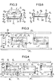
- a support 1 is intended to support a standard integrated circuit box 2 having 28 metal pins 20, to 20 28 .
- An integrated circuit module is encapsulated in the housing 2 and is a memory in CMOS technology of the RAM random access type for example.
- the support 1 is made of a molded plastic and also has a rectangular shape having dimensions substantially larger than those of the housing 2.
- the support 1 also has two longitudinal rows of vertical metal pins 10, at 10 i4 and 10 i5 at 10 28 protruding under the support.
- Each pin 10 1 to 10 28 of the support is terminated at the top by a sheath 11 1 to 11 28 of a known type, for example with flexible conductive strips.
- the sleeve 11 1 to 11 28 is integral with the support 1 in a suitable vertical hole in the support 1 in order to receive by plugging in a respective vertical pin 20, to 20 28 of the housing 2.
- the conductive pins 10 1 to 10 28 are respectively connected by wrapping or soldering to conductors, such as those of a printed circuit board 3.
- each pin 10 1 to 10 28 electrically connects a respective pin 20, to 20 28 to at least one conductor printed on the card 3 such as the conductor 30.
- the support 1 has a U-shaped cross section having branches extending vertically upwards and oriented towards the housing 2.
- the longitudinal branches of the U form longitudinal members 12 1 and 12 2 provided with vertical holes respectively to contain the respective sleeves 11 at 1114 and 11 15 at 11 28 .
- a central cross member 13 0 and two end cross members 13 i and 13 2 of the support 1 connect the side members 12i and 12 2 and form between them two square openings 14i and 14 2 .
- Lights 14, and 14 2 constitute boxes to receive respectively two miniature batteries of the button cell type 4 i and 4 2 forming a backup power source.
- the batteries can be known silver, mercury or, preferably, lithium batteries, commonly used in microelectronics.
- Discoid metal surfaces on the faces of each pile 4 1 , 4 2 constitute a positive terminal , and a negative terminal , from the stack.
- the metal surface of the positive terminal of the battery completely covers one of the faces of the battery and the external cylindrical contour of the battery, while the metal surface of the negative terminal of the battery is a protruding surface concentric to the 'other face of the stack and having a smaller diameter than that of said other face.
- Each battery can be replaced by a miniature storage battery, for example lead or cadmium / nickel.
- the storage battery is then rechargeable by a main supply AP of the printed circuit.
- each elementary emergency power source such as a battery 4 1 , 4 2 is a small waterproof housing and delivers a voltage at most equal to 1.5 volts.
- two batteries placed in series produce a voltage of the order of 2 to 3 volts which can relay a faulty main power source of an integrated circuit.
- the batteries 4 1 and 4 2 are removably mounted in the slots 14, and 14 2 of the support 1 and are connected in series as shown in FIG. 3.
- the positive terminal of the first battery 4 i is connected to an anode of a blocking diode D 1 through a substantially horizontal connecting blade 15 + and a sheath 11 T of a test pin 10 T of the support 1.
- the blade 15 + is a form of stove and is made of semi-rigid or flexible conductive material.
- a circular part of the blade 15 + is underlying the middle of the lumen 14, and supports the discoid terminal .
- a tail of the blade 15 + extends substantially longitudinally and is welded in the vicinity of a lower base of the sheath 11 T of the test pin 10 T located under the cross member 13 1 between the pins 10, and 10 28 .
- the diode D 1 is preferably completely coated in the cross member 13, although, according to another variant, the diode D 1 can be disposed on the cross member 13 1 .
- the anode of the diode D 1 is welded to the sheath 11 ⁇ .
- a cathode of the diode D 1 is welded to the sheath 11 1 of the pin 10 1 .
- the sheath 11 1 receives the pin 20 1 of the housing which forms a positive supply terminal of the integrated circuit.
- the pin 10 i is connected by soldering to a conductor 30 + printed on the card 3 and connected to a positive terminal AP + of the main supply AP of the printed circuit through a blocking diode D 2 on the card 3.
- Diode D 2 has an anode connected to the positive terminal of the main power supply AP and a cathode connected to the negative terminal from the battery 4 1 through the printed conductor 30 + and the diode D 1 .
- a negative supply terminal of the integrated circuit in the housing 2 is constituted by the pin 20 15 diagonally opposite to the positive power supply pin 20 1.
- the pin 20 15 is connected to the negative terminal 402 of the second battery 4 2 also through a connecting blade of semi-rigid or flexible conductive material in the shape of a stove 15 - .
- a circular part of the blade 15 - is underlying the middle of the second lumen 14 2 and receives the negative discoid terminal 402 of the battery 4 2 .
- a tail of the blade 1 5- is bent and is welded to the lower base of the sheath 11 15 of the spindle 10 15 under the girdle 12 2 . As shown in Fig.
- the pin 10 15 is connected by welding to a conductor 30- printed on the card 3, connected directly to a negative terminal AP- or referenced to the ground of the main power supply AP.
- the main power supply AP and the backup power supply 4 1 - 4 2 are thus in parallel between the terminals 20 i and 20 15 via the blocking diodes D 1 and D 2 , which makes it possible to maintain a voltage d '' virtually constant supply in the event of failure of the main supply.
- the negative terminal 40-1 of the first cell 4 1 is connected to the positive terminal + 40 2 of the second cell 4 2 via an electrical connection strip material semi-rigid or flexible conductor 5.
- the strip 5 is rectangular and is arranged longitudinally on either side of the central cross member 130. Two transverse tabs extending downward 51 and in the middle of the strip 5 are inserted in two vertical holes 131 of the central cross member 13 0 and, simultaneously, ends 52 1 and 52 2 of the strip are pressed against the battery terminals 40 - 1 and 40 + 2 . In the support 1, each stack 4 1 , 4 2 is thus held between the respective blade 15 + , 15- and the respective end 52 1 , 52 2 of the strip 5.
- the blades 15 + and 1 5- can be substantially arched upwards, and half-portions of the bar 5 on either side of the tabs 51 can be substantially arched downwards in order to more firmly enclose the stacks.
- the batteries 4 i and 4 2 are substantially thicker than the support 1, which allows a large underside of the housing 2 to be pressed against the strip 5 so that the housing 2 and the support 1 with the batteries form a unitary whole. If necessary, the assembly of the support 1 and of the housing 2 can be consolidated by welding the pins 20 1 to 20 28 to the sleeves 11 1 to 11 28 .
- a measurement of the capacity of the emergency power source 4 1 - 4 2 can be carried out between the test pin 10 T and the pin 10 15 .
- a replacement of the batteries is carried out simply by removing the casing 2 from the support 1, that is to say by removing the pins 20 1 to 20 28 from the sleeves 11 1 to 11 28 , then by raising the bar 5 whose legs 51 are released from the holes 131.
- the removal of the housing 2 is carried out by means of a known multi-spindle extractor forceps.
- the connecting bar 5 passes through the central cross member 13 0 and is fixed to the latter and has ends 52 1 and 52 2 receiving the terminals 40f and 40 - 2 ;
- the connecting blades 15 + and 15- are replaced by two removable blades of the support, similar to a connecting bar shown in FIG. 18, pluggable into pairs of metallized holes of crosspieces 13 1 and 13 2 and covering the terminals 40i and 402, under the housing 2 and above the lights 14 1 and 14 2 ;
- the two pairs of metallized holes are connected to pins 10 i and 10 15 through conductors embedded in the support 1.
- the two plug-in blades can be glued under the housing 2.
- Fig. 1 is also shown a rectangular sheet of insulating material.
- the sheet 54 is arranged horizontally between the support 1 and the circuit board 3 and is crossed by the pins 10 i and 10 28 of the support. After soldering pins 10 1 to 10 28 to card 3 and assembling the housing and the support, as shown in FIG. 2, the blades 15 + and 15- can be substantially pushed towards the card 3.
- the sheet 54 then isolates the blade 15 + in contact with the positive terminal 40 + 1 of the battery 4 1 and the blade 1 5- in contact with the negative terminal 402 of the battery 4 2 with respect to printed conductors of the card 3 located under the support 1.
- the support 1 also has two metallized tracks of supply continuity 16 + and 16-which are fixed on external vertical longitudinal edges of the side members 12 i and 12 2 respectively, and two metal lugs at right angles 17 + and 17- having sides horizontal extending outwardly which are crossed by the vertical power pins 10 1 and 10 15 and welded to them respectively.
- the tracks 16 + and 16- and the lugs 17 + , 17- are provided to rescue several integrated circuit supports not containing a backup power source, by a backup power source contained in another support.
- three integrated circuit supports 1 A, 1 B and 1 C similar to support 1 according to the invention are located between parallel conductors 30 + and 30- of a printed circuit board 3.
- the conductors 30 + and 30- are connected directly to the positive terminal AP + and to the negative terminal AP- of the main power source AP normally supplying the integrated circuits on the support.
- the positive feed pin 10 1 of the support is welded to a first end of a small printed conductor 31 + having a second end opposite the conductor 30 +
- the negative power pin 10 15 of the support is welded to one end of a second small printed conductor 31- having a second end opposite the conductor 30-.
- the main supply AP normally supplies the integrated circuit on the support 1 A through a blocking diode D 2 interconnected to the conductor 30 + and at the second end of the respective conductor 31 + , and through a strap st- connecting the conductor 30 - at the second end of the conductor 31.
- the positive supply terminal of the integrated circuit supported by the support 1 B is connected to the positive terminal AP + of the main supply AP through the elements 11 1 , 10 1 , 17 + and 16 + + of the support 1 B, the strap ST + , the elements 16 + , 17 and 10 1 of the support 1 A, the small conductor 31 + and the diode D 2 relating to the support 1A and the conductor 30 + , and is connected to the positive terminal from the emergency power source 4 1 - 4 2 in the support 1A through the elements 11 1 , 10 1 , 17 + and 16 + of the support 1 B, the strap ST + and the elements 16 + , 17 + , 10 1 , 11 i , D 1 , 11 T and 15 + of support 1A.
- the negative supply terminal of the integrated circuit supported by the support 1 B is connected to the negative terminal AP- of the main supply AP through the elements 11 15 , 10 15 , 17- and 16- of the support 1 B, the strap ST-, the elements 16-, 17- and 10 15 of the support 1 A, the small conductor 31- and the strap st- relative to the support 1 A, and the conductor 30- and is connected to the negative terminal 402 of the emergency power source 4 1 - 4 2 in support 1A through elements 11 15 , 10 15 , 17- and 16- of support 1 B, strap ST- and elements 16-, 17-, 10 15 and 15- from support 1A.
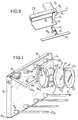
- the connections at pin 10 1 of support 1 A are illustrated in detail in FIG. 5.
- a first solution consists in replacing the strap st + relating to the support 1 C by a blocking diode such as D 2 and in introducing into the support 1 C two miniature backup batteries.
- a second solution consists in removing the straps st + and st - relating to the support 1 C and placing two straps, such as straps ST and ST-, between the tracks 16 + and 16- of the support 1 C and between the tracks 16 + and 16- of a neighboring rescued support, such as support 1B, respectively.
- the conductive tracks 16 + and 16- and the conductive lugs 17 + and 17- of the support according to the invention also serve to manually test each of the batteries contained in the support.
- a support according to the invention can contain four button cells by replacing each cell 4 1 , 4 2 with two thinner cells superimposed and connected in series, as will be seen with reference to FIGS. 11 C and 11D.
- a support can also offer three slots to each receive a thick button cell or a pair of thinner button cells, as will be seen in reference to Figs. 11 E to 11 H.
- a support can also offer two housings each containing three very thin button cells stacked and connected in series. The increase in the number of stacks is done by choosing stacks of different thicknesses.
- the dimensions of the support are adapted to the dimensions of the package of the integrated circuit, and in particular to the number of pins of the package which can for example be equal to 14, 16, 20, 28 or 40, or else to 64 for a microprocessor.
- the lower faces of the slots 14 i and 14 2 can be closed by a molded bottom 140 to form two cavities, as shown diagrammatically in FIG. 6; the bottom 140 replaces the insulating sheet 54 shown in Figs. 1 and 2.
- the horizontal section of the housings such as lights 14 1 , 14 2 or cavities is similar to that of the batteries or accumulators in order to avoid any possible displacement of the batteries or accumulators in the support.
- the bar 5 coupling the batteries 4 1 and 4 2 and shown in FIG. 1 can be replaced by an adhesive copper film which is glued under the housing 2 and the ends of which come into contact with the terminals and 40 + 2 when the pins 20 i to 20 28 are inserted into the sleeves 11 1 to 11 28 .
- two button cells such as the battery 4 2
- two molded circular cavities such as 14a 2 , extending parallel to the large faces of a support 1 a having 28 pins.
- a discoid conductor 52a 2 is printed on a bottom of the cavity 14a 2 or is in the form of a flexible circular metal plate down on the bottom of the cavity 14a 2 .
- the conductor 52a 2 is connected to a similar conductor housed at the bottom of another molded cavity (not shown) through a conductor 5a embedded in the support 1a.
- the cavity 14a 2 has a diameter substantially equal to that of the button cell 4 2 and a height substantially equal to the sum of the thicknesses of the cell 4 2 and of a discoid cover 6 2 both having the same external diameter.
- the closure of the cavity 14a 2 containing the battery by the cover 6 2 is locked by a bayonet assembly.
- Two locking pins 61 and 62 are diametrically opposite and extend from the periphery of the cover facing the cavity 14a 2 .
- An internal face of the cover 6 2 oriented towards the terminal of the battery 4 2 is provided with a printed conductive disc or a flexible circular metal plate 63 fixed to the cover.
- the conductor 63 is extended by a tab 64 disposed underlying the lug 62.
- each groove 143, 144 is formed by a respective slot 141, 142 adapted to receive the pin 61, 62, and another end of each groove forms a stop 145, 146 for the respective pin 61, 62 after rotation a quarter turn of the cover 6 2 .
- a stop 145, 146 for the respective pin 61, 62 after rotation a quarter turn of the cover 6 2 .
- In front of the stop 146 emerges one end of a conductor 15a- in the bottom of the groove 144.
- the conductor 15a is completely encased in the support 1 a and at another end connected to the sheath 11 15 of the negative power pin 10 15 .
- the tab 64 of the cover 6 2 is in contact with the conductor 15a - , which connects the power supply pin 10 15 to the negative terminal 402 of the battery 4 2 .
- a conductor similar to conductor 15a- connects the terminal from the battery 4 1 to the sheath 11T of the test pin 10 T through conductive tabs and discs fixed under a respective cover similar to the cover 6 2 .
- the conductive disks 52a 2 and 63 are preferably flexible conductive plates having opposite own flexions in order to facilitate the removal of the cover, then the extraction from the stack.
- One face of the support 1 a in which the cavities are made, such as the cavity 14a 2 , receiving the batteries 4 i and 4 2 may be the upper face of the support 1 a opposite the case of the integrated circuit 2 or the lower face of the support 1a opposite the printed circuit board 3, in which case the pins 10 1 to 10 28 of the support are long enough to easily access the covers, such as the cover 6 2 shown in FIG. 7.
- This other structure only has a cover, such as the cover 6 2 , closing the corresponding cavity 14a 2 which communicates with the first cavity suitable for receiving the battery 4 i through a corridor having a width at least equal to the diameter of the batteries 4 1 and 4 2 .
- the first cavity has parallel walls formed by the large solid faces of the support 1a.
- the two cavities thus form a continuous oblong cavity, opening outwards only at the level of the open cavity 14a 2 .
- the stack 4 1 is first introduced into the second cavity 14a 2 and then pushed fully into the other cavity through the passage.
- the second stack 4 2 is introduced into the cavity 14a 2 and is covered by the cover 6 2 .
- a small longitudinal hole between the first cavity and a transverse edge of the support 1a lateral to the latter makes it possible to introduce a rod therein to push the stack 4 1 towards the cavity 14a 2 in order to extract the stack 4 1 from the support 1a .
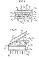
- the button cells 4 1 and 4 2 are arranged vertically and juxtaposed in a single parallelepipedic cavity 14b of a support 1b.
- the axes of the batteries are parallel to the large faces of the housing 2 and to the printed circuit board 3.
- the support 1 b has 14 pins 10 1 to 10 14 with sleeves 11 1 to 11 14 to receive 14 pins 20, to 20 14 d 'an integrated circuit box (not shown).
- the large vertical longitudinal walls of the support 1 b respectively support two rows of pins 10 1 to 10 7 and 10 8 to 10 14 .
- the sheaths of the diagonally opposite pins 10 1 and 10 8 respectively receive the positive supply pins 20, and negative 20 8 of the integrated circuit package.
- the width of the cavity 14b is substantially equal to the thickness of the stacks 4, and 4 2 .
- the batteries are also arranged head to tail.
- the negative terminal of the battery 4 1 and the positive terminal of the battery 4 1 are pressed against the ends of a conductor 5b printed or attached to a large vertical longitudinal face of the cavity 14b, while the positive terminal 40i of the battery 4 1 and the negative terminal of the stack 4 2 are pressed against two respective flexible conductors 15b + and 1 5b- attached to another large vertical longitudinal face of the cavity 14b; the conductor 15b + is connected to the material 11 T of the test pin 10 T and the conductor 15b- is connected to the negative supply pin 10 8 .
- the support 1b has a non-standard thickness substantially greater than the diameter of the button cells.
- the interior of the cavity 14b is accessible from above the support, on the side of the integrated circuit box.
- a cover 6b is articulated on the support 1b by a molded hinge 65 in order to close the cavity 14b and hold the batteries therein in the absence of an integrated circuit box. As shown in Fig. 9, the cover 6b is locked on the top of the support by a ratchet and notch assembly 66. Holes 67 are made in the vicinity of the longitudinal edges of the cover 6b for the free passage of the respective pins 20 1 to 20 14 from the housing to the respective sleeves 11 1 to 11 14 of the support 1 b.
- a support such as support 1b illustrated in Figs. 8 and 9 is generally intended to support an integrated circuit package having 14, 16, 18, 20 or 22 pins.
- Fig. 10 shows a support 1c for supporting an integrated circuit box 2c having two rows of 20 pins 20c, at 20c 20 and 20 C21 at 20c 4 o.
- the support 1 c is made of a molded plastic material and has a parallelepiped shape similar to that of the support 1 shown in FIG. 1.
- the support 1 offers three square lights 14c, 14c 2 and 14c 3 aligned longitudinally between two longitudinal members 12c 1 and 12c 2 and two end crosspieces 13c 1 and 13c 2 , the light 14c 3 being a central light on the support , and separated from the two lights 14c, and 14c 2 by two intermediate crosspieces 13c 3 and 13c 4 .
- Each light 14c 1 , 14c 2 , 14c 3 is suitable for receiving a button cell 4 1 , 4 2 , 4 3 having a diameter substantially smaller than one side of the light. Only the stack 4 2 is shown in FIG. 10.
- the support 1 c comprises two longitudinal rows of vertical metal pins 10c 1 to 10c 20 and 10c 21 to 10c 40 projecting under the side members 12c, and 12c 2 and having vertical sleeves 1 1c 1 to 11c 20 and 11c 21 to 11 c 40 projecting from the side members 12c 1 and 12c 2 .
- the sleeves 11c 1 to 11c 40 are adapted to receive the ends of the pins 20c, to 20c 40 of the integrated circuit box 2c.
- the pins 10ci and 10c 21 diagonally opposite in the support receive the pins 20c, and 20c 21 of the box forming the positive and negative supply terminals of the integrated circuit.
- a rectangular sheet of insulating material 54c is also placed under the support 1c and crossed by the pins 10c 1 to 10c 40 .
- batteries 4 1 , 4 2 and 4 3 are connected in series as shown in FIG. 11 F: batteries 4 1 and 4 3 have positive terminals and oriented upwards, and the battery 4 2 has a positive terminal facing down.
- Two flexible metal connecting bars at right angles 5c 1 and 5c 2 are provided to connect the batteries 4 1 and 4 2 and the batteries 4 3 and 4 2 .
- the bars 5c 1 and 5 2 have horizontal flat wings crossing the middle of the intermediate crossbars 13c 3 and 13c 4 and extending at least to the middle of the slots 14c 1 and 14c 3 and have vertical flat wings extending towards the top near the sleepers 13c 3 and 13c 4 in the lights 14c 3 and 14c 2 , respectively.
- the horizontal wings of the bars 5c 1 and 5c 2 are in contact with small negative terminals and 403 of the stacks 4 1 and 4 3 and support the stacks 4 1 and 4 3
- the vertical wings of the bars 5c 1 and 5c 2 preferably substantially cambered towards the cross member 13c 2 , are applied against the metallic cylindrical contours of the positive terminals and batteries 4 3 and 4 2 , respectively.
- the cell 4 2 is supported by a cylindrical cap 56 of molded insulating material.
- the cover 56 acts as a switch between the emergency power source 4, - 4 3 - 4 2 and the power pins 10c 1 and 10C 21 , in order to activate or not the emergency power supply.
- the cap 56 has a circular bottom against which the large positive terminal is applied of the battery 4 2 .
- a cylindrical wall extending upwards from the cap 56 is notched to form at least two diametrically opposite and flexible cylindrical segments towards the center of the cap or, preferably, as illustrated in FIG. 10, four cylindrical segments 57 diametrically opposite in pairs, in order to enclose the metallic circular periphery of the terminal 40 + 2 .
- the segments 57 have a substantially smaller height than the thickness of the cell 4 2 and the cap 56 has a diameter substantially equal to the outer sides of the square light 14c 2. Under these conditions, the cap 56 with the stack 4 2 can rotate with gentle friction between the internal walls of the lumen 14c 2 , and the small vertical wing of the connecting bar 5c 2 is applied by its own bending sometimes against one insulating segments 57 to disconnect the terminal 40 + 2 of the battery 4 2 relative to the terminal 40 3 of the battery 4 3 , and therefore to deactivate the emergency power supply, sometimes against the circular metal periphery of the terminal 40 2 + to activate the emergency power supply, and therefore connect the batteries 4 1 , 4 3 and 4 2 in series between pins 10c 1 and 10c 21 .
- the grooves 59S and 59H constitute notches for the rotation of the cap 56 and correspond respectively to positions of the segment 57 diametrically opposite the lever 58, at which the segment 57 is on the side of the bar 5c 2 and is in mechanical contact with bar 5 C2 .
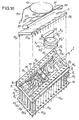
- the support 1 c is associated with a removable cover 9 allowing easy connection and disconnection without soldering of the pins 20c, to 20c 40 of the integrated circuit box 2c relative to the sleeves 11c 1 to 11c 40 of the support 1c of a share, and maintaining the batteries 4 1 , 4 2 and 4 3 in the support 1 in particular in the absence of a housing 2c.
- the cover 9 is a rectangular frame of molded plastic material having a width and length substantially less than that of the support 1 c and formed by two longitudinal members 92 1 and 92 2 and two end cross members 93 1 and 93 2 .
- Two intermediate crosspieces 93 3 and 93 4 share the cover 9 in three square lights 94 1 , 94 3 and 94 2 superimposed on the lights 14c 1 , 14c 3 and 14c 2 .
- the crosspieces 93 1 to 93 4 have an upward convex section, for example trapezoidal as shown in FIG. 10, so that the side members 92 1 and 92 2 are only applied against the support 1 c, that is to say on the side members 12c, and 12c 21 when the cover 9 covers the support 1 c.
- the cover 9 is then framed by thin longitudinal walls 121 and 122 at the periphery of the support 1c, extending upwards the side members 12c 1 and 12c 2 and having ends forming straight corners at the four corners of the support.
- two flexible locking tabs 98 1 and 98 2 extend vertically downwards under the middle of the end crosspieces 93 1 and 93 2 and have pairs of upper horizontal ribs 981 1 , 981 2 and lower 982 1 , 982 2 outwards to cooperate with central vertical grooves inwards 130 1 and 130 2 and rectangular orifices 131 1 and 131 2 formed in the crosspieces 13c 1 and 13c 2 respectively.
- the orifices 131 1 and 132 2 are respectively in the middle of the end crosspieces 13c 1 and 13c 2 , and the vertical distance between two lower and upper ribs of each tab 98 and 98 2 is equal to the half thickness of the crosspieces 13c 1 and 13c 2 .
- the legs 98 i and 98 2 slide in the grooves 130 1 and 130 2 open towards the openings 14c, and 14c 2 , and the pairs of ribs 981, - 982 1 and 981 2 - 982 2 enclose central parts of the crosspieces 13c1 and 13c 2 above the orifices 131 1 and 131 2 when the cover 9 is applied against the support 1 in order to lock the cover to the support, as shown in FIG. 12.
- each sheath such as the sheath 11 c 21 , is constituted by two vertical conductive strips, here parallel to the walls 121 and 122, having a height less than that of the holes 91 1 to 9140.
- the lower ribs 982 1 and 982 2 of the tabs 98 1 and 98 2 first penetrate into the orifices 131 1 and 131 2 respectively, and the blades of the sleeves 11 1 to 11 40 penetrate with gentle friction through the flared ends of the holes 91 1 to 91 40 .
- the external longitudinal sides of the longitudinal members 92 1 and 92 2 are vertical and slide between the walls 121 and 122. Then the housing 2c covers the cover 9 so that the pins 20ci to 20c 40 penetrate vertically by upper flared ends of the holes 91 1 to 91 4 and slide between the blades of the sheaths 11c 1 to 11c 40 respectively.
- Vigorous pressure is finally exerted downwards on the casing 2c so that the upper ribs 981 1 and 981 2 penetrate into the orifices 131 1 and 131 2 and the lower ribs 982 1 and 982 2 pass under the crosspieces 13c 1 and 13c 2 .
- the cross members 93 1 to 93 4 of the cover tend to flatten and the side members 92 1 and 92 2 are more apart and are pressed against the walls 121 and 122 of the support.
- the spacing of the longitudinal members 92 1 and 92 2 pushes substantially the blades of the sheaths 11c 1 to 11c 40 which firmly pinch the ends of the pins 20c, to 20c 40 and which establish real mechanical and electrical contacts with them. Ci, without using solder.
- the cover 9 and the housing 2c are firmly held in superposition on the support 1c. Whenever the housing 2c is to be placed on the cover 9 or to be removed from the latter, the sliding of the pins 20c 1 to 20c 40 in the sleeves 11 c 1 to 11 C40 confers self-cleaning of these electrical contact elements .
- a special fork tool allows the lower ribs 982 1 and 982 2 to be released upwards from the underside of the crossbeams 13c, and 13c 2 which then penetrate into the orifices 131 1 and 1312.
- the ascent of the legs 98 i and 98 2 is facilitated by the proper bending of the cross members 93 1 to 93 4 becoming more convex and of the walls 121 and 122 becoming vertical again, the casing 2c can be removed without the batteries are necessarily removed, since the cover 9 is still locked to the support thanks to the lower ribs 982 1 and 982 2 retained in the orifices 131 1 and 131 2 .
- the removal of one or more batteries is obtained by completely pulling up the cover 9 in order to release the ribs 982 1 and 982 2 from the orifices 131 1 and 132 2 .
- the legs 98 i and 98 2 and the sets with grooves and slots 130, - 131 1 and 130 2 - 131 2 are replaced by two vertical cylindrical legs 99 under adjacent to the crosspieces 93 1 and 93 2 and two vertical cylindrical holes 132 in the middle of the crosspieces 13c 1 and 13c 2 , as shown in FIG. 13.
- Each tab 99 has a vertical diametric slot 990, perpendicular to the crosspieces 93 1 , 93 2 and a conical end stud 991 converging downwards surmounted by a flange 992. As shown in Figs.
- a locking ring 133 is attached to one end su of each hole 132 and fixed therein.
- the ring 133 has an annular groove 134 with a conical lower end.
- the hole 132 can be blind or offer a lower end 135 having a diameter smaller than the major part remaining of the hole in order to form a cylindrical chamber 136 under the ring 133.
- In the chamber 136 is provided a washer 137 with a flared upper end.
- the diameters of the bores in the ring 133 and the washer 137 are less than the diameter of the stud 991 and substantially equal to the width of the stud when the branches separated by the slot 990 are completely pressed against each other, as shown in Figs . 14A and 14C.
- the section of the elements 99, 133 and 137 and the corresponding bores and holes can be square or polygonal for example.
- a third downward pressure on the housing 2c causes the engagement of the pins 991 in the washers 137 (Fig. 14C).
- the opposite clean flexions of the branches on either side of the slot 990 of each tab 93 allow the respective flange 992 to temporarily secure the tab 99 with the respective washer 137.
- the trigger elastic of the crosspieces 93 1 to 93 4 of the cover upwards drives the tabs 99 and therefore the washers 137 which slide in the chambers 136 and abut against the rings 133 (FIG. 14D).
- the washers 137 fall back to the bottom of the chambers 136 and the pins 991 then mount in the rings 133 until the flanges 992 penetrate into the grooves 134 thanks to the widening of the slots 990 (FIG. 14E).
- the box 2c can then be removed from the cover 9.
- the cover 9 comprises two flexible conductive connecting strips 95 + and 95-, and a blocking diode D i .
- the blades 95 + and 95- extend longitudinally from the middle of the crosspieces 93, and 93 2 and in the slots 94, and 94 2 to be applied to the positive terminal 40; of the battery 4 1 and the negative terminal 402 of the battery 4 2 respectively, as shown in FIG. 11 F.
- the diode D 1 is completely embedded in the cross member 93, between the hole 91, and the blade 95 + .
- a conductor partially embedded in the cross member 93, connects the strip 95 + to the anode of the diode D 1 , and has an elbow 91 T emerging towards the outside from the middle of the cross member 93 1 , as shown in Figs. 10 and 15.
- the 91 T elbow is used as a test terminal, like the 10 T pin in Fig. 1.
- the cathode of diode D 1 is connected to a conductor 138 1 embedded in the cross member 93, and having a flat vertical end directed downward 139 1 emerging under the cross member 93 1 near the hole 91 1 , as shown in Figs. 10 and 15.
- the connecting strip 95- is connected to a conductor 138 2 embedded in the cross member 93 2 and having a vertical flat end 139 2 emerging under the cross member 93 2 near the hole 91 21 , as shown in Fig. 16.
- the ends 139 1 and 139 2 are intended to be respectively applied to contact blades 111, and 1112 of the sleeves 11c 1 and 11c 2 of the supply pins 10c 1 and 10c 21 , as shown in FIG. 12.
- the contact blade 111 1 , 111 21 is cut from one of the two blades of the sheath 11c 1 , 11c 21 just above the feed pin 10c 1 , 10c 21 and is arched substantially upwards.
- the terminal 40i of the battery 4 i is connected to the positive supply pin 10c 1 through the test terminal 91 T , the diode D 1 , the conductor 138 1 , the end 139 1 of the conductor 138 1 and the contact blade 111 1 of the sheath 11 c 1 , and the terminal 402 of the battery 4 2 is connected to the negative power pin 10c 21 through the conductor 138 2 , the end 139 2 of the conductor 138 2 and the contact blade 111 21 of the sheath 11c 21 .
- the structure of the support 1c as described above can be adapted to the shape, the mutual arrangement of the terminals of each cell and to the dimensions, such as thickness, of the cells.
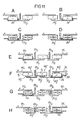
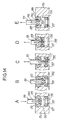
- Figs. 11 A to 11H Various examples of adaptation are shown in Figs. 11 A to 11H.
- the support 1 c contains three button cells each having a small projecting metallic circular surface for positive terminal, analogous to the negative terminals 40 1 to 40 3 of the batteries 4 1 to 4 3 , and a large metallic cylindrical surface for negative terminal, analogous to positive terminals at batteries 4 1 to 4 3 ; in this case, the cap 56 forming a switch receives the negative terminal of a battery housed in the light 14c 1 , and the connecting bars 5c 1 and 5c 2 are turned 180 °; grooves 59S and 59H are also provided in the cross member 13c 1 to receive the lever 58, as shown in FIG.
- Figs. 11 G and 11 H correspond respectively to Figs. 11 E and 11 F by replacing each battery with two button batteries half as thick as the batteries in Figs. 11 E and 11 F; in this case, the square connecting bars 5c 2 according to FIG. 11 E and 5c 1 according to FIG. 11 F are replaced respectively by connecting bars 5c 2 'and 5c 1 ' each having a vertical portion passing through the corresponding intermediate cross member 13c 4 and 13c 3 and two horizontal portions at the ends of the vertical portion to be applied from below and from above against the terminals of the lower and upper thin batteries in the adjacent lights 14c 2 and 14c 3 , 14c 1 and 14c 3 .
- Figs. 11 A to 11 D are shown supports having only two reads miers 14ci and 14c 2 each containing one or two stacks respectively arranged in a manner analogous to the end stacks in Figs. 11 E to 11 H.
- connecting bars instead of connecting bars being secured to the support 1 d, connecting bars can be secured to the intermediate crosspieces 93 3 and 93 4 of the cover 9.
- each of the lights 14c, 14c 3 and 94, 94 3 can be barred by a thin longitudinal or transverse cross member or has a bottom coming from molding in order to form cavities to receive the batteries.
- the switch for the emergency power source can be a longitudinal or vertical slide with a metallized end replacing the cover 56.
- FIG. 18 A first variant of the support 1 according to said other embodiment is illustrated in FIG. 18.
- the support 1 has a general shape analogous to the support already described with reference to FIG. 1, although according to another variant, the support can be analogous to the support 1c shown in FIG. 10.
- the positive terminal 40 + 2 of the cell 4 2 being placed above the negative terminal 40, of the cell 4 1 .
- the positive terminal of the lower battery 4 1 is connected to the power supply pin 10 1 of the support through the conductive connecting blade 15 + in the form of a stove and the diode D 1 , the test pin 10 T being eliminated.
- the terminal 40 1 + is also connected through a conductor 15 T to a test terminal BT of the monitoring circuit 7 which is housed in the second light 14 2 , as will be seen below.
- the conductor 1 5T is preferably embedded in the support and bypasses the light 14, through the cross member 13 1 , the spar 12 2 and the central cross member 13 0 .
- the bar 5 of FIG. 1 is replaced by a similar bar comprising only the longitudinal half-portion between the end 52 i and the two legs extending downward 51.
- the horizontal end 52 is applied against the negative terminal of the upper pile 4 2 and presses the batteries 4 1 and 4 2 against the blade 15 + when the two tabs 51 are inserted in the two holes 131, here metallized, of the central cross member 13 0 .
- the holes 131 are connected to the negative supply pin or referenced to the earth 10 15 of the support 1 and to a ground terminal BG of the circuit 7 through a conductor 15G preferably embedded in the support and bypassing the light 14 2 to through the cross member 13 0 and the beam 12 2 .
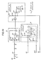
- the block diagram of the monitoring circuit 7 is shown in FIG. 19.
- the circuit 7 essentially comprises a voltage-controlled oscillator 70 oscillating at a variable frequency in the range of audible frequencies, a control circuit 71 controlling the oscillator 70, and a signaling circuit 72.
- the oscillator 70 comprises a Schmitt trigger circuit 701 with feedback resistance 702 and with variable capacitor in the form of a varicap diode 703 connected to the terminal BG.
- An input of the oscillator is constituted by a terminal 704 common to the resistor 702 and to the vericap diode 703.
- the terminal 704 is connected to the test terminal BT, and therefore to the positive terminal from the backup source 4 1 - 4 2 , through a resistor 73 in series with a directly polarized diode 74.
- the frequency of the signal at an output 705 of the trigger circuit 701 is inversely proportional to the RC parameter of the constant resistance 702 and the variable capacitance of the varicap 703 diode, and is therefore inversely proportional to the voltage applied to the LV test terminal.
- the control circuit 71 consists essentially of a flip-flop 711 of the RS type. An input R of flip-flop 711 is connected to a reset terminal BRZ of circuit 7. Another input S of flip-flop 711 is connected to a validation terminal BV of circuit 7. An output Q of flip-flop 711 is connected to a trigger input 706 of the trigger circuit 701.
- the terminals BV and BRZ as well as an output terminal BS of the circuit 7 are connected to a microprocessor (not shown) implanted on the printed circuit board 3 through respective conductors 1 5 v , 15 RZ and 15 S embedded in the support 1 at the level of the second light 14 2 and through respective additional pins 10 v , 10 RZ and 10 s , as shown in FIG. 18.
- the microprocessor or other equivalent circuit makes it possible to interrogate the monitoring circuit in order to signal a discharge from the emergency source.
- the interrogation is carried out when the microprocessor does not perform other priority tasks, or periodically depending on the organization of the other circuits located on the printed card.
- the interrogation by the microprocessor is transmitted in the form of a fugitive negative pulse to the BRZ terminal in order to initialize the flip-flop 711. Then periodically, a fugitive negative pulse is applied to the terminal BV by the microprocessor in order to validate the circuit trigger 701 by applying a “1” to input 706. If the voltage from the backup source to the LV terminal is greater than the predetermined voltage threshold, typically equal to 2.5 volts for two batteries operating normally each with 1, 5 volts, the oscillator 70 remains blocked and no oscillating signal is detected by the microprocessor at the output BS.
- the predetermined voltage threshold typically equal to 2.5 volts for two batteries operating normally each with 1, 5 volts
- an audible frequency signal is delivered by the terminal 705 from the oscillator 70 to the terminal BS and energizes signaling circuit 72.
- Circuit 72 warns that the backup source will soon fail, the predetermined voltage threshold being chosen to be significantly higher than the minimum voltage for maintaining the backup source.
- the state of the BRZ terminal is not changed by the microprocessor in response to the oscillating signal. Otherwise, the microprocessor delivers a fleeting pulse on the BRZ terminal to reset the flip-flop 711 which blocks the oscillator 70, which avoids any untimely discharge of the backup source 4, - 4 2 .
- the signaling circuit 72 comprises an electro-acoustic transducer 721 such as a miniature loudspeaker in the form of a buzzer with a piezoelectric bar. Terminals 722 and 723 of the transducer 721 are connected to the terminal referenced to earth BG and, through an inverter 724, to terminals 705 and BS, respectively.
- the circuit 70 can comprise a display device 725, such as a strip of liquid crystals or light-emitting diodes. The display device is then connected between the output 70 of the oscillator 70 and the terminal BS connected to the input of the inverter 724.
- the monitoring circuit 7 also includes other elements, such as bias resistors 712, 713 and 726 connected respectively to the terminals BRZ, BV and BS and brought to a positive voltage by a common terminal BP.
- the BP terminal is connected to the card 3 through a conductor 15p embedded in the support 1 as shown in FIG. 18.
- the monitoring circuit 7 can be manufactured in the form of an integrated circuit enclosed in a housing or in the hybrid form of discrete elements implanted on a small printed circuit board.
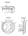
- Figs. 20, 21 and 22 illustrate an exemplary embodiment of the housing of the monitoring circuit 7 constituted by an insulating discoid base 75 and a metallic or plastic cylindrical cover 76.
- a support 77 of the integrated or discrete monitoring circuit 7 is bonded to an internal face of the base 75.
- Six small vertical conductive tails constitute the terminals BG, BS, BV, BP, BRZ and BT and are plugged into respective metallized holes of a bottom of the light 14 2 of the support 1, here forming a receptacle circular of the case 75-76 typically having a diameter of 2.5 cm.
- the preceding metal holes constitute the ends of the conductors 15 G , 15s, 15v, 15p, 15 RZ and 15r.
- the tails of the housing 75-76 relating to the terminals BS, BV, BP and BRZ replace the pins 10s, 10v, 10 P and 10 RZ and pass through the bottom of the cavity 14 2 .
- In a part of the circular periphery of the cover 76 are provided holes for the location of the display device 725, such as light-emitting diodes shown in FIGS. 21 and 22.
- the piezoelectric buzzer 721 can constitute the major part of the top of the cover 76 and have its terminals 722 and 723 in the form of wires housed in the housing and welded to the support 77, as shown in FIGS. 20 and 21.
- the buzzer 721 containing the inverter 724 is pressed onto an adhesive tape 780 secured to a U-shaped clamp 78. Legs bent downwards 781 of the clamp 78 are hooked at the ends of the integrated circuit box 2.
- the terminals 722 and 723 of the buzzer consist of flexible wires welded or pinched to the pins 10 15 and 10 s of the support 1.
- a common control circuit 71 monitors a large number of emergency power sources, for example six AS, at AS 6 .
- Each power source AS 1 to AS 6 is housed in the first light 14, of a respective support 1 1 to 1 6 of an integrated circuit box similar to the support 1 shown in FIG. 18.
- the second light 14 2 of the support in the form of a cavity includes a hybrid or integrated monitoring circuit 7 1 to 7 6 comprising an oscillator 70 i to 70 6 , a resistor 73 1 to 73 6 and a diode 74, to 74 6 similar to those described with reference to FIG. 19, as well as other elements 727 1 to 727 6 , 728, to 728 6 , and 729 1 to 729 6 .
- the hybrid or integrated circuit also includes a display device 725 1 to 725 6 , such as light-emitting diodes or a strip of liquid crystals interconnected between the positive terminal BP and the output 705 1 to 705 6 of the oscillator 70, to 70 6 through an inverter 727 1 to 727 6 and a resistor 728 1 to 728 6 .
- a non-inverting element 727 ′, at 727 ′ 6 and the display device 725 1 to 725 6 can be suitably connected in series to the ground terminal BG according to another variant shown in FIG. 24.
- One of the supports 1 1 to 1 6 also includes control circuit 71 with RS flip-flop 711, piezoelectric buzzer 721, two switches 714 and 715 and two bias resistors 716 and 717.
- the Q output of flip-flop 711 is connected to trigger inputs 706 1 to 706 6 of oscillators 70, to 70 6 .
- the terminal 723 of the common buzzer 721 is connected to the outputs 705 1 to 705 6 of the oscillators 70, to 70 6 through switches 729 1 to 729 6 .
- Switches 729 1 to 729 6 , 714 and 715 are doors in CMOS technology.
- the different connections between the six circuits 7 1 to 7 6 supported by the supports are made through support pins and conductors of the printed circuit board 3.
- the operation of the monitoring circuit shown in FIG. 23 is as follows.
- a fugitive negative pulse applied to the BRZ terminal initializes the flip-flop 711 which closes the gates 714 and 715.
- a validation pulse applied to the BV terminal changes the state of the flip-flop 711 which validates the trigger circuits 701 1 to 701 6 des oscillators 70, to 70 6 and opens the doors 714 and 715.
- a second input of the door 714 being connected to the positive voltage terminal BP through the resistor 716, an output of the door 714 applies a positive voltage to inputs of the doors 729, to 729 6 and to another input of door 715.
- doors 729 1 to 729 6 are connected respectively to the outputs 705 1 to 705 6 of the oscillators 70 i to 70 6 . If no emergency power source AS 1 to AS 6 produces a voltage below the predetermined voltage threshold, doors 729 1 to 729 6 and 715 remain closed and the voltage at the output terminal BS is not modified.
- an audible frequency signal is delivered by output 705 1 to 705 6 of the corresponding oscillator 70, to 70 6 .
- the audible frequency signal activates the illumination of the corresponding display device 725 1 to 725 6 and opens the corresponding door 729 1 to 729 6 at the rate of the audible frequency.
- the positive voltage applied by the door 714 excites the buzzer 721 through the corresponding door 729 1 to 729 6 .
- the output BS of the door 715 presents at the rate of the audible frequency of the voltages referred to the ground.
- the alternating signal at the output BS is then processed by the microprocessor and indicates a voltage anomaly in one of the six emergency power sources AS 1 to AS 6 .
- a monitoring circuit comprises all of the circuits 7 1 to 7 6 of FIG. 23 and is completely supported by the same support such as the support relating to circuit 7 i , which then comprises five test pins connected through the printed board to the positive terminals of the power sources AS 2 to AS 6 included in the other five supports.
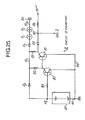
- the integrated or hybrid circuit box 75-76 in the cavity 14 2 of the support 1 shown in FIGS. 18 and 20 to 22 also includes an inhibition circuit 8.
- Circuit 8 inhibits a predetermined function of the integrated circuit contained in the housing 2 when the voltage of the main power source AP disappears. If the integrated circuit in the housing 2 is a memory, the predetermined function to be inhibited is the authorization to write to the memory, for example.
- the muting circuit 8 comprises two NPN transistors 80 and 81 having transmitters connected to the terminal BG referred to the ground. Collectors of the transistors 80 and 81 are connected respectively through resistors 82 and 83 to the common terminal of the blocking diodes Di and D 2 already mentioned with reference to FIG. 3.
- the collector of transistor 80 is connected to a base of transistor 81.
- a base of transistor 80 is connected to the positive voltage terminal AP + of the main power source AP to be monitored, through a resistor 84 and a pin additional (not shown) of the support 1.
- the collector of the transistor 81 is connected to the terminal BP through a diode 85 and a resistor 86.
- An anode of the diode 85 and a terminal of the resistor 86 is designated by a common terminal 87 to be connected to a function inhibit input of the integrated circuit of the housing 2 through an additional pin (not shown) of the support 1.
- the main power source AP When the main power source AP normally delivers a voltage, the positive voltage at the AP + terminal saturates the first transistor 80 and blocks the second transistor 81. The voltage on the collector of transistor 81 is positive, which produces no mass active at terminal 87.
- the backup source 4 1 - 4 2 relays the main source AP by applying a supply voltage through the diode D 1 .
- the disappearance of the positive voltage at the AP + terminal blocks the transistor 80.
- the positive voltage on the collector of the transistor 80 saturates the second transistor 81 and the diode 85 becomes conductive.
- An active ground is thus present at terminal 87 which controls the inhibition of the predetermined function of the integrated circuit in the housing 2.
Landscapes
- Chemical & Material Sciences (AREA)
- Chemical Kinetics & Catalysis (AREA)
- Electrochemistry (AREA)
- General Chemical & Material Sciences (AREA)
- Engineering & Computer Science (AREA)
- Microelectronics & Electronic Packaging (AREA)
- Battery Mounting, Suspending (AREA)
- Lead Frames For Integrated Circuits (AREA)
Claims (50)


Applications Claiming Priority (2)
| Application Number | Priority Date | Filing Date | Title |
|---|---|---|---|
| FR8315150A FR2552590B1 (fr) | 1983-09-23 | 1983-09-23 | Support de boitier de circuit integre |
| FR8315150 | 1983-09-23 |
Publications (2)
| Publication Number | Publication Date |
|---|---|
| EP0136237A1 EP0136237A1 (de) | 1985-04-03 |
| EP0136237B1 true EP0136237B1 (de) | 1987-06-03 |
Family
ID=9292480
Family Applications (1)
| Application Number | Title | Priority Date | Filing Date |
|---|---|---|---|
| EP19840401898 Expired EP0136237B1 (de) | 1983-09-23 | 1984-09-21 | Halterung für Gehäuse für eine integrierte Schaltung |
Country Status (5)
| Country | Link |
|---|---|
| US (1) | US4633239A (de) |
| EP (1) | EP0136237B1 (de) |
| JP (1) | JPS6091658A (de) |
| DE (1) | DE3464109D1 (de) |
| FR (1) | FR2552590B1 (de) |
Families Citing this family (12)
| Publication number | Priority date | Publication date | Assignee | Title |
|---|---|---|---|---|
| MX167287B (es) * | 1987-11-23 | 1993-03-15 | Lancer Corp | Aparato para controlar el crecimiento de un banco de hielo alrededor de un aparato de enfriamiento |
| US5038467A (en) * | 1989-11-09 | 1991-08-13 | Advanced Interconnections Corporation | Apparatus and method for installation of multi-pin components on circuit boards |
| US4985989A (en) * | 1989-11-09 | 1991-01-22 | Advanced Interconnections Corporation | Method and apparatus for removing a multi-pin component installed in sockets on a circuit board |
| JP2681109B2 (ja) * | 1989-11-14 | 1997-11-26 | 山一電機株式会社 | 電気部品用接続器 |
| US5287617A (en) * | 1992-08-11 | 1994-02-22 | Advanced Interconnections Corporation | Apparatus for extracting an integrated circuit package installed in a socket on a circuit board |
| JPH08179698A (ja) * | 1994-12-20 | 1996-07-12 | Niles Parts Co Ltd | 表示装置の組立構造及び組立方法 |
| US6992378B2 (en) * | 2000-12-30 | 2006-01-31 | Intel Corporation | Socket and package power/ground bar apparatus that increases current carrying capacity resulting in higher IC power delivery |
| JP2002275976A (ja) * | 2001-03-21 | 2002-09-25 | Toto Ltd | 圧送装置 |
| US7088074B2 (en) * | 2002-01-02 | 2006-08-08 | International Business Machines Corporation | System level device for battery and integrated circuit integration |
| EP1691431A1 (de) * | 2005-02-14 | 2006-08-16 | SAT Akkumulatoren Technik AG | Verbindungselement zur Verbindung von Zellen zu Akkumulatoren |
| EP2942739A1 (de) * | 2014-05-07 | 2015-11-11 | Siemens Aktiengesellschaft | Halterung für RFID-Transponder, RFID-Transponder und Betätigungswerkzeug |
| CN115347302B (zh) * | 2022-08-17 | 2024-07-19 | 广州小鹏汽车科技有限公司 | 底盖组件和圆柱电池 |
Family Cites Families (11)
| Publication number | Priority date | Publication date | Assignee | Title |
|---|---|---|---|---|
| US2748328A (en) * | 1953-12-14 | 1956-05-29 | Premier Res Lab Inc | Combination pronged base for electrical devices |
| US2782389A (en) * | 1954-01-11 | 1957-02-19 | Motorola Inc | Subminiature tube receptacle |
| US3289045A (en) * | 1964-03-02 | 1966-11-29 | Intellux Inc | Circuit module |
| US3634600A (en) * | 1969-07-22 | 1972-01-11 | Ceramic Metal Systems Inc | Ceramic package |
| BE757101A (fr) * | 1969-10-06 | 1971-03-16 | Grisby Barton Inc | Assemblage de relais |
| FR2445630A1 (fr) * | 1969-10-15 | 1980-07-25 | Amerace Corp | Connecteur pour plaquette porte-circuit |
| US3880493A (en) * | 1973-12-28 | 1975-04-29 | Burroughs Corp | Capacitor socket for a dual-in-line package |
| US4245877A (en) * | 1976-12-30 | 1981-01-20 | Burndy Corporation | Circuit package receptacle with movable base separation means |
| US4107400A (en) * | 1977-06-24 | 1978-08-15 | Timex Corporation | Battery hatch cover |
| GB2084769B (en) * | 1980-08-06 | 1985-03-13 | Racal Microelect System | Back-up electrical power supply |
| JPS58500829A (ja) * | 1981-05-27 | 1983-05-19 | マステク、コ−パレイシヤン | 集積回路に関連して使用される電池収容装置及びの製造方法 |
-
1983
- 1983-09-23 FR FR8315150A patent/FR2552590B1/fr not_active Expired
-
1984
- 1984-09-21 EP EP19840401898 patent/EP0136237B1/de not_active Expired
- 1984-09-21 DE DE8484401898T patent/DE3464109D1/de not_active Expired
- 1984-09-21 US US06/652,977 patent/US4633239A/en not_active Expired - Fee Related
- 1984-09-25 JP JP59198759A patent/JPS6091658A/ja active Pending
Also Published As
| Publication number | Publication date |
|---|---|
| DE3464109D1 (en) | 1987-07-09 |
| EP0136237A1 (de) | 1985-04-03 |
| US4633239A (en) | 1986-12-30 |
| JPS6091658A (ja) | 1985-05-23 |
| FR2552590B1 (fr) | 1986-03-28 |
| FR2552590A1 (fr) | 1985-03-29 |
Similar Documents
| Publication | Publication Date | Title |
|---|---|---|
| EP0136237B1 (de) | Halterung für Gehäuse für eine integrierte Schaltung | |
| EP0121467B1 (de) | Kleinstverbinder mit hoher Kontaktdichtheit | |
| EP0013718B1 (de) | Drehbar gelagerter Träger für gedruckte Schaltungen | |
| FR2930849A3 (fr) | Prise electrique multiple de securite. | |
| CA2948387C (fr) | Dispositif cutane, notamment generateur d'impulsions pour l'electrostimulation | |
| CA2949344C (fr) | Connecteur electrique notamment pour dispositif cutane. | |
| CH656025A5 (fr) | Connecteur electrique. | |
| CH678670A5 (de) | ||
| FR2582441A1 (fr) | Dispositif pour supporter une multiplicite de condensateurs | |
| EP0024364A1 (de) | Vorrichtung zum Halten einer Batterie in einer elektronischen Armbanduhr | |
| EP0123595A1 (de) | Eingabe/Ausgabe-Gerät für eine programmierbare automatische Einrichtung, Serie von solchen Geräten und Verfahren zur Realisierung ihrer Verbindungsanschlüsse | |
| EP0081795A1 (de) | Elektrischer Verbinder mit mehrfacher Kupplung und Verwendung desselben in mehrfachen Messverbindern für Schaltungsplatte von einem in einem Rahmen montierten elektronischen Gerät | |
| FR2946491A1 (fr) | Dispositif electrique a declenchement automatique par soulevement. | |
| FR2560059A1 (fr) | Jouet produisant des sons | |
| EP4124871B1 (de) | Vorrichtung und verfahren zum testen von elektronischen chips | |
| EP2312965B1 (de) | Struktur zum transport und gebrauch von tragbaren geräten mit insbesondere elementen, die unter verwendung von drahtverbindungen miteinander verbunden werden können, wie tragbare multimediengeräte | |
| FR2759207A1 (fr) | Dispositif de sortie electrique permettant une connexion avec differents types de prises males | |
| FR2495348A1 (fr) | Boitier de mecanisme d'une pendule a pile | |
| WO2022111996A1 (fr) | Interface electromecanique pour systeme automatique de gestion de batteries d'un drone | |
| FR2627049A1 (fr) | Ensemble combine formant retenue de chassis et contact electrique pour appareil alimente par piles ou accumulateurs | |
| CA2948293C (fr) | Dispositif medical cutane comprenant une partie principale avec une embase et une electrode amovible | |
| FR2748608A1 (fr) | Systeme electronique pour batterie bipolaire et carte pour ce systeme | |
| FR3138704A1 (fr) | Enregistreur acoustique sous-marin | |
| EP3145579B1 (de) | Gerät für die haut mit einem biegbaren gebiet und mit mitteln zur begrenzung der biegbarkeit | |
| EP0135438A1 (de) | Anschliessbares elektrisches Gehäuse |
Legal Events
| Date | Code | Title | Description |
|---|---|---|---|
| PUAI | Public reference made under article 153(3) epc to a published international application that has entered the european phase |
Free format text: ORIGINAL CODE: 0009012 |
|
| AK | Designated contracting states |
Designated state(s): DE FR GB |
|
| 17P | Request for examination filed |
Effective date: 19850918 |
|
| 17Q | First examination report despatched |
Effective date: 19861028 |
|
| GRAA | (expected) grant |
Free format text: ORIGINAL CODE: 0009210 |
|
| AK | Designated contracting states |
Kind code of ref document: B1 Designated state(s): DE FR GB |
|
| REF | Corresponds to: |
Ref document number: 3464109 Country of ref document: DE Date of ref document: 19870709 |
|
| PLBE | No opposition filed within time limit |
Free format text: ORIGINAL CODE: 0009261 |
|
| STAA | Information on the status of an ep patent application or granted ep patent |
Free format text: STATUS: NO OPPOSITION FILED WITHIN TIME LIMIT |
|
| 26N | No opposition filed | ||
| PGFP | Annual fee paid to national office [announced via postgrant information from national office to epo] |
Ref country code: GB Payment date: 19890831 Year of fee payment: 6 |
|
| PGFP | Annual fee paid to national office [announced via postgrant information from national office to epo] |
Ref country code: FR Payment date: 19890927 Year of fee payment: 6 |
|
| PGFP | Annual fee paid to national office [announced via postgrant information from national office to epo] |
Ref country code: DE Payment date: 19891003 Year of fee payment: 6 |
|
| PG25 | Lapsed in a contracting state [announced via postgrant information from national office to epo] |
Ref country code: GB Effective date: 19900921 |
|
| GBPC | Gb: european patent ceased through non-payment of renewal fee | ||
| PG25 | Lapsed in a contracting state [announced via postgrant information from national office to epo] |
Ref country code: FR Effective date: 19910530 |
|
| PG25 | Lapsed in a contracting state [announced via postgrant information from national office to epo] |
Ref country code: DE Effective date: 19910601 |
|
| REG | Reference to a national code |
Ref country code: FR Ref legal event code: ST |