EP0136238A1 - Vorrichtung zur Messung der Nähe einer metallisch leitenden Oberfläche - Google Patents
Vorrichtung zur Messung der Nähe einer metallisch leitenden Oberfläche Download PDFInfo
- Publication number
- EP0136238A1 EP0136238A1 EP84401906A EP84401906A EP0136238A1 EP 0136238 A1 EP0136238 A1 EP 0136238A1 EP 84401906 A EP84401906 A EP 84401906A EP 84401906 A EP84401906 A EP 84401906A EP 0136238 A1 EP0136238 A1 EP 0136238A1
- Authority
- EP
- European Patent Office
- Prior art keywords
- sensor
- coil
- sensors
- signal
- magnetic circuit
- Prior art date
- Legal status (The legal status is an assumption and is not a legal conclusion. Google has not performed a legal analysis and makes no representation as to the accuracy of the status listed.)
- Granted
Links
Images


Classifications
-
- G—PHYSICS
- G01—MEASURING; TESTING
- G01B—MEASURING LENGTH, THICKNESS OR SIMILAR LINEAR DIMENSIONS; MEASURING ANGLES; MEASURING AREAS; MEASURING IRREGULARITIES OF SURFACES OR CONTOURS
- G01B7/00—Measuring arrangements characterised by the use of electric or magnetic techniques
- G01B7/28—Measuring arrangements characterised by the use of electric or magnetic techniques for measuring contours or curvatures
- G01B7/287—Measuring arrangements characterised by the use of electric or magnetic techniques for measuring contours or curvatures using a plurality of fixed, simultaneously operating transducers
-
- B—PERFORMING OPERATIONS; TRANSPORTING
- B23—MACHINE TOOLS; METAL-WORKING NOT OTHERWISE PROVIDED FOR
- B23K—SOLDERING OR UNSOLDERING; WELDING; CLADDING OR PLATING BY SOLDERING OR WELDING; CUTTING BY APPLYING HEAT LOCALLY, e.g. FLAME CUTTING; WORKING BY LASER BEAM
- B23K9/00—Arc welding or cutting
- B23K9/12—Automatic feeding or moving of electrodes or work for spot or seam welding or cutting
- B23K9/127—Means for tracking lines during arc welding or cutting
- B23K9/1272—Geometry oriented, e.g. beam optical trading
- B23K9/1276—Using non-contact, electric or magnetic means, e.g. inductive means
Definitions
- the present invention relates to a device intended to measure the proximity of a conductive metal surface by means of at least one eddy current sensor disposed opposite the surface.
- This device finds its application in techniques related to robotics.
- a device can be used as a profile detector in a robotic assembly installation, and as a joint detector in an automatic welding machine.
- the processing circuit generates a continuous signal which is a function of the phase difference between the signal delivered by each coil and a reference signal derived from the power supply oscillator thereof.
- This measurement technique does not allow the nature of the metal to be overcome, since the measured phase difference is not independent of the variations in the eddy current losses according to the metals opposite.
- Such a device overcomes the difficulty of balancing the coils which each work in turn.
- the measurement is slowed down compared to the previous device, due to the time required to establish the current in the coils when switching from one coil to another.
- the subject of the present invention is precisely a device for measuring the proximity of a conductive metal surface which does not have the drawbacks of the devices according to the prior art and which makes it possible in particular to perform a reluctance measurement in air, which allows to overcome the permeability of the metal and the heating in the measurement of proximity.
- the device comprises at least one eddy current sensor arranged opposite the surface, each sensor comprising at least one coil, a sinusoidal voltage source supplying said sensor, means for processing the sinusoidal signal delivered by the sensor, characterized in that said processing means comprise means for measuring the inductive component alone of the impedance of said coil. So that the measured reluctance is not the reluctance in the metal, but the reluctance in the air, we also use a source delivering a voltage whose frequency is greater than 100 kHz (and at least higher than the desired accuracy is greater).
- the means for measuring the inductive component of the signal are synchronous detection means, the reference signal being a signal of the same frequency as the sinusoidal signal supplying the sensors, out of phase with respect to this signal of a determined angle (0 or n / 2 depending on the sensor).
- the filtering of the synchronous detection is done by integration means, operating in synchronism with said reference signal, during a determined whole number of periods of this signal.
- means are also provided for automatically correcting the gain and the offset voltage of the proximetric signal.
- These automatic gain and offset correction means may in particular include memories in which they are recorded, for each sensor, the corrections to be made.
- one or more control sensors can be placed in a fixed position relative to a reference surface, these sensors being connected to the memories so that the evolution of their characteristics makes it possible to correct the contents of the memories. This control sensor must in practice be of the same nature as the sensors used directly for the measurement.
- the proximetric signals after gain and offset correction, are preferably introduced into an analog-digital converter, then they send a Linearization memory to which a calibration curve is recorded.
- the source comprises an oscillator and means for controlling said oscillator in amplitude and in frequency.
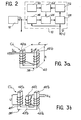
- the sensor coil is mounted on a U-shaped magnetic circuit open in the direction of said surface, said source being connected directly to the terminals of the coil, and the sinusoidal signal delivered by The sensor being obtained from the current flowing through the coil by means of a low-impedance current-voltage transformer.
- the senor comprises an E-shaped magnetic circuit open in the direction of said surface, a transmitting coil mounted on one of the end branches and a receiving coil partially wound on The other end branch and partly on the intermediate branch, said source being connected to the terminals of the transmitting coil, and the sinusoidal signal delivered by the sensor being obtained by putting in opposition the signals induced in the two parts of the coil. receptor.
- the senor comprises an H-shaped magnetic circuit, an excitation coil mounted on the intermediate branch of the magnetic circuit, a receiver coil mounted on the end branches of the magnetic circuit and a reference conducting plane disposed at a given distance opposite the parts of the end branches situated on the side opposite to the surface whose proximity it is desired to measure, said source being connected to the terminals of the excitation coil.
- the device according to the invention When the device according to the invention is applied to the detection of the profile of a conductive metal surface, it comprises at least one series of aligned eddy current sensors, said source simultaneously supplying the sensors, multiplexing means being provided for successively injecting into the processing means each of the signals delivered by the sensors.
- the invention also relates to a proximity sensor with eddy currents, characterized in that it comprises an E-shaped magnetic circuit open in the direction of a metallic object whose one wishes to measure proximity, a transmitting coil mounted on one of the end branches and a receiving coil wound partly on the other end branch and partly on the intermediate branch and connected in opposition.
- the invention also relates to a proximity sensor with eddy currents, characterized in that it comprises several juxtaposed elementary sensors, each elementary sensor comprising at least one coil with currents FoucauLt mounted on a magnetic circuit open in the direction of a metal object whose proximity is to be measured, the elementary sensors being juxtaposed so that their magnetic circuits are arranged in parallel planes.
- the invention also relates to a multipoint proximity sensor comprising metal plates arranged between elementary sensors, serving as shielding between them and as a guide for the field lines of so as to channel the magnetic flux in the direction of the object to be detected.
- the profile detector device mainly consists of a sinusoidal voltage source 10 supplying in parallel n eddy current sensors C 1 to C n aligned in series and arranged opposite the profile to be detected.
- the signals i 1 to i n delivered by the latter can be transmitted to a multiplexer 14 either directly or through n buffer stages T 1 to T n which then transform the signals i 1 to i n in voltage signals u 1 to u n .
- the output of the multiplexer 14 is successively switched to each of its inputs by a sequencer 16, itself activated by a crenellated signal and of constant frequency U emitted by an oscillator 18 serving as will be seen later to slave in frequency and phase Le sinusoidal signal U delivered by the voltage source 10.
- the signal u i leaving the multiplexer 14 is injected into a synchronous detector 20-22 controlled by the crenellated signal U c and comprising a multiplier 20 outputting a signal u d whose characteristics will be analyzed later.
- This signal u d is filtered in a filtering circuit 22 also controlled by the sequencer 16.
- the analog signal u delivered by the circuit 22 is then converted into a digital signal, then linearized by circuits also controlled by the sequencer 16 and represented diagrammatically by block 24 in FIG. 1.
- the number of outputs of circuits 24 making it possible to display the digital signal S is determined according to the subsequent operation which must be done for calculator. For example, the circuits 24 will include eight outputs if the subsequent operation must be done on a computer working on eight bits.
- the voltage source 10 comprises an oscillator 26, controlled in frequency, in phase and in amplitude.
- a power amplifier 28 supplied by the oscillator 26 delivers a sinusoidal voltage U of constant frequency and amplitude, so as not to disturb the precision of the device.
- the amplitude control of the oscillator 26 is achieved by means of a reference voltage source 30.
- the amplitude of the signal U delivered by the amplifier 28 is detected by an amplitude detector 32 and compared with The reference voltage delivered by the source 30 in a comparator 34, the output of which acts on the oscillator 26, so as to correct the amplitude of the signal delivered by the latter.
- the sinusoidal supply voltage U of the sensor coils thus has a constant amplitude. Consequently, the flow is forced which contributes to ensuring the independence of each sensor from neighboring sensors.
- phase of the sinusoidal signal U delivered by the amplifier 28 is compared with the phase of a signal serving as a reference in a phase comparator 36 whose output acts on the oscillator 26, in order to correct the frequency of the signal applied by the latter to the power amplifier 28.
- the frequency reference used to control in frequency and phase The signal delivered by the oscillator 26 is given by the oscillator 18 delivering the signal Uc injected to the synchronous detector 20 and serving to control the sequencer 16 as we have previously seen with reference to Figure 1. This eliminates the noise that would be produced by random switching.
- the oscillator 18 is preferably an oscillator controlled by quartz.
- the phase comparator 36 makes it possible to permanently maintain between the sinusoidal signal U used to supply the sensors C 1 to C n and the reference signal U delivered by the oscillator 18 a phase shift ⁇ constant. Due to the good frequency stability of the signal U c delivered by the oscillator 18, the frequency stability of the sinusoidal signal U delivered by the voltage source 10 is thus ensured.
- the phase shift ⁇ established by the phase comparator 36 between the signals U and U is fixed so as to measure only the variations in inductance of the sensor coil.
- this phase shift is worth ; in the case of the sensor described with reference to FIG. 3b, it is worth 0.
- the inductance is the only quantity dependent only on the distance separating the sensor from the metallic surface and almost - independent of temperature.
- the frequency of the sinusoidal signal U used to supply the coils of the sensors is chosen so that the electromagnetic wave emitted by the sensors does not penetrate a metallic sheet Calumi- nium, iron, various alloys, copper, etc ...) of more than 1 / 10th of mm.
- the choice of a low penetration thickness makes it possible to overcome the permeability of the metal, the defects within its structure, its nature and its temperature.
- the voltage control of the sinusoidal signal U supplying the sensors C 1 to C n makes it possible to establish in them a forced flux which does not depend on the proximity of a sheet.
- the current i 1 to i n delivered by each of the sensors C 1 to C n can then be measured in module and in phase.
- each of the sensors of a series of sensors C 1 to C n has an original structure giving its magnetic circuit a directive character making them practically insensitive to a metallic mass offset with respect to La direction thus defined.
- the series of sensors can include complementary elements serving as shielding between the sensors and against electromagnetic interference of external origin and making it possible to improve the range of each of the sensors.
- each sensor C. comprises a magnetic core 38 in the shape of a U and a coil 40.
- these sensors have a small thickness e allowing high axial resolution along the profile to be detected. In addition, this reduced size does not diminish their scope in any way.
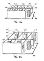
- the sensors C 1 to C n are aligned opposite the profile to be detected, so that the planes passing through the axes of each of the branches 42a and 42b of each sensor are parallel to each other.
- immunity to electromagnetic interference of external origin and the independence between sensors can be improved by having on either side of the series of aligned sensors of the metal plates 44, and by disposing between the sensors of the metal plates. 46.
- These plates 46 and 44 are supported by a plate 48 disposed behind the series of sensors, on the side opposite the ends of the branches 42a and 42b opposite which the surface of which the profile is to be detected is located.
- the range of the sensors for given dimensions thereof can be increased by having between each of the branches 42a and 42b of the same sensor a metal plate 50.
- this plate makes it possible to remove the field lines which go directly from one pole to another, so that the Field Lines are lengthened.
- these plates 50 can in particular be supported by plates 46, of which they must be electrically isolated.
- the online association of sensors - C 1 to C n significantly modifies the characteristics.
- the simultaneous and phase excitation of all the sensors allows a significant improvement in the range. Indeed, at a certain distance from the line of sensors, the magnetic field is equivalent to that which would be created by a linear magnetic circuit and decreases according to a law in 1 / x 2 according to the axis x which extends parallel to the branches 42a and 42b of the sensors, while it decreases according to a Law in 1 / x 3 for an isolated sensor.
- the consequence of this phenomenon is better focusing of the emitted magnetic field lines; therefore a better concentration of the flow, When one moves away from the sensors.
- the range of the sensors is therefore increased, as is their directivity.
- each sensor C ' i comprises a magnetic core 38' in the shape of an E, a transmitting coil 41 'wound on the end branch 42'a of the core 38' and a receiving coil in two parts 43'a and 43'b wound respectively on the other end branch 42'b and on the intermediate branch 42'c of the core 38 '.
- the winding of the two parts 43'a and 43'b of the receiver winding on the branches 42'b and 42'c is carried out in the opposite direction, as illustrated in FIG. 3b.
- the sensor C'i shown in FIG. 3b is such that the flow passing through the emitting branch 42'a closes, being divided between the two branches 42'b and 42'c.
- each of the branches 42'a, 42'b and 42'c is preferably chosen so that the output voltage is zero when there is no sheet metal in front of the sensor. This characteristic makes it possible to increase the sensitivity of the sensor for distant sheets, and therefore its range.
- the variant of Figure 3b has the same advantages as the variant of Figure 3a.
- it makes it possible to locate the Field Lines approximately in a plane passing through the axes of the three branches of the core 38 ′ and it has a minimum size for a given range and a high axial resolution.
- the sensor of Figure 3b has the advantage of being of differential type, which gives it good stability in temperature and over time.
- the sensors C ' 1 to C' n are arranged in an aligned series, in the same way as the sensors C 1 to C n in the variant embodiment of FIG. 4a.
- metal plates 44 ′ and 46 ′ acting as shields are preferably arranged around the sensors and fixed to a plate 48 ′.
- plates 50 ′ can be placed between the branches 42 ′ a and 42 ′ c of each sensor, in order to increase their range.
- each sensor C “ i comprises a magnetic core 38" in the form of an H
- an excitation coil 41 "wound on the intermediate branch 38" has a core 38 "and a receiving coil 43" wound on each of the others branches 38 “b and 38” c of the core 38 ", on either side of the intermediate branch 38" a.
- the winding of the take-up reel 43 "on the branches 38" b and 38 "c is carried out in the opposite direction.
- Each of the sensors C “i of the line of sensors thus makes it possible to carry out a differential measurement which promotes the rejection of any drifts.
- the structure described makes it possible to associate this difference with a quotient, which leads to reducing the dynamic variations observed on the difference. Compared to U-shaped sensors such as that of FIG. 3a, the non-linearity of the response of the sensor is thus reduced and the sensitivity is increased.
- the line of sensors C "1 to C" n can be carried out in a manner comparable to that which has been described for the sensors Ci and C'i with reference to FIGS. 4a and 4b.
- the coil b i of the sensor C i (coil 40). Thanks to the use of a voltage source 10 controlled in frequency, in phase and in amplitude, The coil b i is supplied with a constant voltage U. According to the invention, The coil b i is traversed by a current i the variations of which are representative of the only variations in the impedance of the coil generated by the variations in the distance separating the sensor from the metal surface opposite.
- the buffer stage which is associated with each of the sensors C 1 to C n When these are produced in accordance with the variant embodiment of FIG. 3a has the double function of transforming the current signal i into a voltage signal u i and adjust the voltage level so that it is zero when there is no sheet metal in front of the sensor.
- the current i passing through the coil b i is injected into a current-voltage converter 52 and a capacitance c i is mounted in parallel on each of the coils b i .
- the capacitance c i has the effect of adding a constant to the demodulated signal, a constant which is adjusted so as to obtain a zero demodulated voltage when there is no sheet in front of the sensor.
- This feature has two advantages. First of all, it reduces the current supplied by the amplifier, since the coil and the capacity then form a tuned plug circuit. It also makes it possible to improve the dynamics and the precision of the device, since the continuous component around which the signal varies varies is removed.
- the input impedance of the converter 52 is very low, which makes it possible to keep the supply voltage U constant at the terminals of the coil.
- each of the voltage signals u i leaving the converters 52 in the variant embodiment of FIG. 3a or leaving directly from the sensor C ' i in the variant embodiment of FIG. 3b are injected into the multiplexer 14 which transmits them in turn to the synchronous detector 20 under the action of the sequencer 16.
- the multiplexer 14 is of the analog type with n inputs. It is controlled by the sequencer 16, constituted by a synchronous control logic of the crenellated signal U c , to eliminate the effect of a random phase shift on the transient regimes.
- each of the signals u i is phase shifted by ⁇ i and it is the inductive component in quadrature u i sin ⁇ i which characterizes the distance separating the corresponding sensor from the opposite surface, with respect to the signal U supplying the sensors.
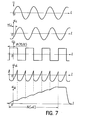
- the crenellated signal U delivered by the oscillator 18 has the same frequency as the signal U and therefore that each of the signals u i , but it has a phase shift ⁇ , preferably equal to , with respect to the signal U.
- the multiplier 20 which simultaneously receives the signals u i and U c , has the function of multiplying these signals one by the other in order to deliver a signal u d corresponding to the signal u i during the positive half-periods of the signal U and inversely of the signal u i during the negative half-periods of the signal U c . It is clear that the average value of the resulting signal is proportional to the quadrature component u i sin ⁇ i of the signal delivered by the sensor.
- the signal u d is introduced into a filter 22 consisting mainly of an integrator 54 associated with an input switch 56 and a reset switch 58. More precisely, the signal u d is injected into the negative input of the integrator 54 through the switch 56.
- the reset switch 58 is mounted in parallel on the capacity C of the integrator 54. The positive input of the integrator is connected to Earth.
- the switches 56 and 58 are controlled by the sequencer 16, so as to operate the integrator 54 for an integer N of periods of the signal u d and to reset the system to zero before injecting a signal u d corresponding to a other sensor.
- the appearance of the signal u s thus obtained is represented in FIG. 7.
- the value of the signal u obtained after a number N of periods is representative of the quadrature component u i sin ⁇ i of the signal u i delivered by each sensors and, consequently, the distance separating these sensors from the opposite surface.
- the analog DC voltage signal u thus obtained at the output of the integrator 54 must then be converted to digital, in order to be used subsequently in particular by an eight-bit computer. As illustrated in FIG. 8, this conversion is carried out by an analog-digital converter 60. Preferably, to this converter is added an automatic gain and offset correction system as well as a linearization system.
- the gain and offset correction system also shown in FIG. 8, includes two memories 62 and 64 in which the corrections are recorded.
- This recording of the offset and gain corrections respectively in memories 62 and 64 is carried out during a prior calibration of the system carried out once and for all.
- the digital offset correction signal recorded in the memory 62 for a given sensor is converted into analog in a digital-analog converter 66, before being added to the signal u corresponding to this sensor in an adder 68. Furthermore, the digital gain correction signal recorded in memory 64 and corresponding to this same sensor is transformed into analog in a second digital-analog converter 70, before being injected into the analog-digital converter 60 to correct the gain.
- memories 62 and 64 are controlled by the sequencer 16 simultaneously with the multiplexer 14 and the filtering integrator 54.
- the signal leaving the converter 60 is used to address a linearization memory 72 in which a calibration curve has been recorded beforehand. This curve is obtained during the calibration by memorizing the non-linear relationship between the distance D
Landscapes
- Physics & Mathematics (AREA)
- Engineering & Computer Science (AREA)
- Geometry (AREA)
- Plasma & Fusion (AREA)
- Mechanical Engineering (AREA)
- General Physics & Mathematics (AREA)
- Measurement Of Length, Angles, Or The Like Using Electric Or Magnetic Means (AREA)
- Investigating Or Analyzing Materials By The Use Of Magnetic Means (AREA)
- Geophysics And Detection Of Objects (AREA)
- Transmission And Conversion Of Sensor Element Output (AREA)
Applications Claiming Priority (2)
| Application Number | Priority Date | Filing Date | Title |
|---|---|---|---|
| FR8315323A FR2552540B1 (fr) | 1983-09-27 | 1983-09-27 | Dispositif pour mesurer la proximite d'une surface metallique conductrice |
| FR8315323 | 1983-09-27 |
Publications (2)
| Publication Number | Publication Date |
|---|---|
| EP0136238A1 true EP0136238A1 (de) | 1985-04-03 |
| EP0136238B1 EP0136238B1 (de) | 1989-03-08 |
Family
ID=9292566
Family Applications (1)
| Application Number | Title | Priority Date | Filing Date |
|---|---|---|---|
| EP19840401906 Expired EP0136238B1 (de) | 1983-09-27 | 1984-09-25 | Vorrichtung zur Messung der Nähe einer metallisch leitenden Oberfläche |
Country Status (4)
| Country | Link |
|---|---|
| EP (1) | EP0136238B1 (de) |
| JP (1) | JPS6095304A (de) |
| DE (1) | DE3477055D1 (de) |
| FR (1) | FR2552540B1 (de) |
Cited By (3)
| Publication number | Priority date | Publication date | Assignee | Title |
|---|---|---|---|---|
| WO1997021070A1 (en) * | 1995-12-05 | 1997-06-12 | Skf Condition Monitoring | Driver for eddy current proximity probe |
| EP1659399A3 (de) * | 2004-11-19 | 2006-08-09 | General Electric Company | Verfahren und Vorrichtung zum Testen eines Bestandteils |
| CN113825981A (zh) * | 2019-05-15 | 2021-12-21 | 德纳汽车系统集团有限责任公司 | 传感器系统及其温度补偿方法 |
Families Citing this family (7)
| Publication number | Priority date | Publication date | Assignee | Title |
|---|---|---|---|---|
| FR2572175A1 (fr) * | 1984-10-24 | 1986-04-25 | Stein Heurtey | Procede et dispositif pour mesurer l'epaisseur de couches metalliques minces deposees sur un support conducteur |
| FR2699665B1 (fr) * | 1992-12-23 | 1995-02-10 | Careno Jean Francois | Capteur inductif de position à sortie numérique. |
| DE4410987A1 (de) * | 1994-03-30 | 1995-10-05 | Foerster Inst Dr Friedrich | Hochauflösende Wirbelstromsonde |
| US5854553A (en) * | 1996-06-19 | 1998-12-29 | Skf Condition Monitoring | Digitally linearizing eddy current probe |
| FR3009076B1 (fr) * | 2013-07-26 | 2017-03-31 | Michelin & Cie | Systeme de mesure de l'epaisseur d'une couche de gomme d'un pneumatique |
| JP6095063B2 (ja) * | 2013-07-31 | 2017-03-15 | 日立Geニュークリア・エナジー株式会社 | 渦電流探傷プローブ |
| JP6283965B2 (ja) * | 2016-03-18 | 2018-02-28 | 長野県 | 検査装置、検査方法及び非接触式センサ |
Citations (6)
| Publication number | Priority date | Publication date | Assignee | Title |
|---|---|---|---|---|
| US3309539A (en) * | 1963-08-06 | 1967-03-14 | Bethlehem Steel Corp | Phase detector circuit |
| FR2083038A5 (en) * | 1970-01-21 | 1971-12-10 | British Steel Corp | Detection of strip shape deviation - in ferro-magnetic strip material |
| US3703097A (en) * | 1970-12-24 | 1972-11-21 | Kaiser Aluminium Chem Corp | Method and system for measuring sheet flatness |
| FR2424515A1 (fr) * | 1978-04-27 | 1979-11-23 | Nippon Kokan Kk | Appareil d'exploration automatique pour determiner le contour d'un objet metallique |
| EP0064454A1 (de) * | 1981-04-30 | 1982-11-10 | COMMISSARIAT A L'ENERGIE ATOMIQUE Etablissement de Caractère Scientifique Technique et Industriel | Verfahren zum lateralen Positionieren eines Gliedes bezüglich einer zwischen zwei metallischen Oberflächen formierten und mit Unterbrechungen versehenen Fuge |
| FR2507310A1 (fr) * | 1981-06-04 | 1982-12-10 | Commissariat Energie Atomique | Procede pour determiner le profil d'une surface metallique conductrice, procede pour comparer ce profil a un profil modele et dispositif pour la mise en oeuvre de ces procedes |
-
1983
- 1983-09-27 FR FR8315323A patent/FR2552540B1/fr not_active Expired
-
1984
- 1984-09-25 DE DE8484401906T patent/DE3477055D1/de not_active Expired
- 1984-09-25 EP EP19840401906 patent/EP0136238B1/de not_active Expired
- 1984-09-27 JP JP59200701A patent/JPS6095304A/ja active Pending
Patent Citations (6)
| Publication number | Priority date | Publication date | Assignee | Title |
|---|---|---|---|---|
| US3309539A (en) * | 1963-08-06 | 1967-03-14 | Bethlehem Steel Corp | Phase detector circuit |
| FR2083038A5 (en) * | 1970-01-21 | 1971-12-10 | British Steel Corp | Detection of strip shape deviation - in ferro-magnetic strip material |
| US3703097A (en) * | 1970-12-24 | 1972-11-21 | Kaiser Aluminium Chem Corp | Method and system for measuring sheet flatness |
| FR2424515A1 (fr) * | 1978-04-27 | 1979-11-23 | Nippon Kokan Kk | Appareil d'exploration automatique pour determiner le contour d'un objet metallique |
| EP0064454A1 (de) * | 1981-04-30 | 1982-11-10 | COMMISSARIAT A L'ENERGIE ATOMIQUE Etablissement de Caractère Scientifique Technique et Industriel | Verfahren zum lateralen Positionieren eines Gliedes bezüglich einer zwischen zwei metallischen Oberflächen formierten und mit Unterbrechungen versehenen Fuge |
| FR2507310A1 (fr) * | 1981-06-04 | 1982-12-10 | Commissariat Energie Atomique | Procede pour determiner le profil d'une surface metallique conductrice, procede pour comparer ce profil a un profil modele et dispositif pour la mise en oeuvre de ces procedes |
Cited By (7)
| Publication number | Priority date | Publication date | Assignee | Title |
|---|---|---|---|---|
| WO1997021070A1 (en) * | 1995-12-05 | 1997-06-12 | Skf Condition Monitoring | Driver for eddy current proximity probe |
| EP1659399A3 (de) * | 2004-11-19 | 2006-08-09 | General Electric Company | Verfahren und Vorrichtung zum Testen eines Bestandteils |
| US8013599B2 (en) | 2004-11-19 | 2011-09-06 | General Electric Company | Methods and apparatus for testing a component |
| CN113825981A (zh) * | 2019-05-15 | 2021-12-21 | 德纳汽车系统集团有限责任公司 | 传感器系统及其温度补偿方法 |
| US20220221307A1 (en) * | 2019-05-15 | 2022-07-14 | Dana Automotive Systems Group, Llc | Sensor system and a method of temperature-compensation thereof |
| CN113825981B (zh) * | 2019-05-15 | 2025-01-21 | 德纳汽车系统集团有限责任公司 | 传感器系统及其温度补偿方法 |
| US12429359B2 (en) | 2019-05-15 | 2025-09-30 | Dana Automotive Systems Group, Llc | Sensor system and a method of temperature-compensation thereof |
Also Published As
| Publication number | Publication date |
|---|---|
| FR2552540A1 (fr) | 1985-03-29 |
| DE3477055D1 (en) | 1989-04-13 |
| JPS6095304A (ja) | 1985-05-28 |
| EP0136238B1 (de) | 1989-03-08 |
| FR2552540B1 (fr) | 1987-03-20 |
Similar Documents
| Publication | Publication Date | Title |
|---|---|---|
| EP0117790B1 (de) | Wirbelstrom-Multispulen-Sensor versehen mit einer Spulenausgleichvorrichtung | |
| EP2417443B1 (de) | Vorrichtung zur zerstörungsfreien überprüfung einer elektrisch leitenden struktur | |
| EP0179720B1 (de) | Verfahren und Vorrichtung zur Dickenmessung von dünnen, auf einen leitenden Träger aufgebrachten, metallischen Schichten | |
| EP0136238B1 (de) | Vorrichtung zur Messung der Nähe einer metallisch leitenden Oberfläche | |
| EP0146091B1 (de) | Verfahren und System zur zerstörungsfreien Prüfung durch Wirbelströme unter Verwendung von überstreichenden Frequenzen | |
| EP0141724A2 (de) | Regeleinrichtung zum selbsttätigen Ausrichten eines Laserstrahls | |
| FR2648236A1 (fr) | Appareil de mesure d'impedance surfacique | |
| EP0147294B1 (de) | Vorrichtung und Verfahren zum dynamischen kontaktlosen Messen kleiner Abstände | |
| EP0717265A1 (de) | Magnetischer Kodierer zur Markierungslesung einer magnetischen Spur | |
| FR2504838A1 (fr) | Procede de positionnement lateral d'un organe par rapport a un joint forme entre deux surfaces metalliques et presentant des discontinuites | |
| EP0622610A1 (de) | Verfahren und Anordnung zum Eichen der Dickenmessanordnung des Querprofils eines flächigen Gutes | |
| EP1671140B1 (de) | Vorrichtung zur messung eines magnetfeldes | |
| EP0492394B1 (de) | Gerät zur zerstörungsfreien Untersuchung mit Wirbelströmen mit Umschaltung zur Flussaddition-Flusssubtraktion | |
| EP3430443A1 (de) | Induktive faktor-1-sensorvorrichtung | |
| EP0492392B1 (de) | Gerät zur zerstörungsfreien Prüfung mit Wirbelströmen | |
| EP2307897B1 (de) | Magnetfeld-messeinrichtung und verfahren | |
| FR2537716A1 (fr) | Dispositif de mesure automatique et sans contact du volume d'une couche deposee sur un substrat | |
| WO2001001097A1 (fr) | Capteur de couple a barrette de hall | |
| EP1020728B1 (de) | Anordnung zum messen eines Stromes in einer Leitung | |
| EP0061401B1 (de) | Verfahren und Gerät zum lateralen Positionieren eines Organs in bezug auf eine Unterbrechung zwischen zwei verlagerten metallischen Flächen | |
| FR2662812A1 (fr) | Dispositif de detection d'un champ magnetique utilisant un circuit magnetique en alliage magnetique doux et systeme de regulation d'un champ magnetique comportant ce dispositif. | |
| FR2712975A1 (fr) | Procédé de contrôle non destructif d'un tube mince par courants de Foucault et capteur à courants de Foucault. | |
| FR2618548A1 (fr) | Dispositif de detection de position d'un objet soumis a un deplacement lineaire | |
| FR2679658A1 (fr) | Dispositif statique de controle non destructif par courants de foucault de produits metalliques longs defilant a grande vitesse par creation d'un champ tournant axial. | |
| FR2638837A1 (fr) | Procede de detection de la derive en temperature du signal de reponse d'un capteur inductif et dispositif pour sa mise en oeuvre |
Legal Events
| Date | Code | Title | Description |
|---|---|---|---|
| PUAI | Public reference made under article 153(3) epc to a published international application that has entered the european phase |
Free format text: ORIGINAL CODE: 0009012 |
|
| AK | Designated contracting states |
Designated state(s): DE FR GB IT SE |
|
| 17P | Request for examination filed |
Effective date: 19850912 |
|
| 17Q | First examination report despatched |
Effective date: 19870306 |
|
| R17C | First examination report despatched (corrected) |
Effective date: 19870615 |
|
| RAP1 | Party data changed (applicant data changed or rights of an application transferred) |
Owner name: COMMISSARIAT A L'ENERGIE ATOMIQUE |
|
| GRAA | (expected) grant |
Free format text: ORIGINAL CODE: 0009210 |
|
| AK | Designated contracting states |
Kind code of ref document: B1 Designated state(s): DE FR GB IT SE |
|
| REF | Corresponds to: |
Ref document number: 3477055 Country of ref document: DE Date of ref document: 19890413 |
|
| ITF | It: translation for a ep patent filed | ||
| GBT | Gb: translation of ep patent filed (gb section 77(6)(a)/1977) | ||
| PLBE | No opposition filed within time limit |
Free format text: ORIGINAL CODE: 0009261 |
|
| STAA | Information on the status of an ep patent application or granted ep patent |
Free format text: STATUS: NO OPPOSITION FILED WITHIN TIME LIMIT |
|
| 26N | No opposition filed | ||
| PGFP | Annual fee paid to national office [announced via postgrant information from national office to epo] |
Ref country code: SE Payment date: 19910813 Year of fee payment: 8 |
|
| PGFP | Annual fee paid to national office [announced via postgrant information from national office to epo] |
Ref country code: DE Payment date: 19910831 Year of fee payment: 8 |
|
| PGFP | Annual fee paid to national office [announced via postgrant information from national office to epo] |
Ref country code: GB Payment date: 19910924 Year of fee payment: 8 |
|
| ITTA | It: last paid annual fee | ||
| PGFP | Annual fee paid to national office [announced via postgrant information from national office to epo] |
Ref country code: FR Payment date: 19920922 Year of fee payment: 9 |
|
| PG25 | Lapsed in a contracting state [announced via postgrant information from national office to epo] |
Ref country code: GB Effective date: 19920925 |
|
| PG25 | Lapsed in a contracting state [announced via postgrant information from national office to epo] |
Ref country code: SE Effective date: 19920926 |
|
| GBPC | Gb: european patent ceased through non-payment of renewal fee |
Effective date: 19920925 |
|
| PG25 | Lapsed in a contracting state [announced via postgrant information from national office to epo] |
Ref country code: DE Effective date: 19930602 |
|
| PG25 | Lapsed in a contracting state [announced via postgrant information from national office to epo] |
Ref country code: FR Free format text: LAPSE BECAUSE OF NON-PAYMENT OF DUE FEES Effective date: 19940531 |
|
| REG | Reference to a national code |
Ref country code: FR Ref legal event code: ST |
|
| EUG | Se: european patent has lapsed |
Ref document number: 84401906.7 Effective date: 19930406 |