EP0136454B1 - Dispositif pour la dissipation de chaleur des plaquettes à circuit imprimé - Google Patents
Dispositif pour la dissipation de chaleur des plaquettes à circuit imprimé Download PDFInfo
- Publication number
- EP0136454B1 EP0136454B1 EP84108975A EP84108975A EP0136454B1 EP 0136454 B1 EP0136454 B1 EP 0136454B1 EP 84108975 A EP84108975 A EP 84108975A EP 84108975 A EP84108975 A EP 84108975A EP 0136454 B1 EP0136454 B1 EP 0136454B1
- Authority
- EP
- European Patent Office
- Prior art keywords
- printed circuit
- housing
- heat
- dissipation
- projections
- Prior art date
- Legal status (The legal status is an assumption and is not a legal conclusion. Google has not performed a legal analysis and makes no representation as to the accuracy of the status listed.)
- Expired
Links
Images
Classifications
-
- H—ELECTRICITY
- H05—ELECTRIC TECHNIQUES NOT OTHERWISE PROVIDED FOR
- H05K—PRINTED CIRCUITS; CASINGS OR CONSTRUCTIONAL DETAILS OF ELECTRIC APPARATUS; MANUFACTURE OF ASSEMBLAGES OF ELECTRICAL COMPONENTS
- H05K7/00—Constructional details common to different types of electric apparatus
- H05K7/20—Modifications to facilitate cooling, ventilating, or heating
- H05K7/2039—Modifications to facilitate cooling, ventilating, or heating characterised by the heat transfer by conduction from the heat generating element to a dissipating body
- H05K7/205—Heat-dissipating body thermally connected to heat generating element via thermal paths through printed circuit board [PCB]
-
- H—ELECTRICITY
- H05—ELECTRIC TECHNIQUES NOT OTHERWISE PROVIDED FOR
- H05K—PRINTED CIRCUITS; CASINGS OR CONSTRUCTIONAL DETAILS OF ELECTRIC APPARATUS; MANUFACTURE OF ASSEMBLAGES OF ELECTRICAL COMPONENTS
- H05K1/00—Printed circuits
- H05K1/02—Details
- H05K1/0201—Thermal arrangements, e.g. for cooling, heating or preventing overheating
- H05K1/0203—Cooling of mounted components
- H05K1/0209—External configuration of printed circuit board adapted for heat dissipation, e.g. lay-out of conductors, coatings
-
- H—ELECTRICITY
- H05—ELECTRIC TECHNIQUES NOT OTHERWISE PROVIDED FOR
- H05K—PRINTED CIRCUITS; CASINGS OR CONSTRUCTIONAL DETAILS OF ELECTRIC APPARATUS; MANUFACTURE OF ASSEMBLAGES OF ELECTRICAL COMPONENTS
- H05K7/00—Constructional details common to different types of electric apparatus
- H05K7/20—Modifications to facilitate cooling, ventilating, or heating
- H05K7/2039—Modifications to facilitate cooling, ventilating, or heating characterised by the heat transfer by conduction from the heat generating element to a dissipating body
- H05K7/20436—Inner thermal coupling elements in heat dissipating housings, e.g. protrusions or depressions integrally formed in the housing
-
- H—ELECTRICITY
- H05—ELECTRIC TECHNIQUES NOT OTHERWISE PROVIDED FOR
- H05K—PRINTED CIRCUITS; CASINGS OR CONSTRUCTIONAL DETAILS OF ELECTRIC APPARATUS; MANUFACTURE OF ASSEMBLAGES OF ELECTRICAL COMPONENTS
- H05K7/00—Constructional details common to different types of electric apparatus
- H05K7/20—Modifications to facilitate cooling, ventilating, or heating
- H05K7/20536—Modifications to facilitate cooling, ventilating, or heating for racks or cabinets of standardised dimensions, e.g. electronic racks for aircraft or telecommunication equipment
- H05K7/20545—Natural convection of gaseous coolant; Heat transfer by conduction from electronic boards
-
- H—ELECTRICITY
- H05—ELECTRIC TECHNIQUES NOT OTHERWISE PROVIDED FOR
- H05K—PRINTED CIRCUITS; CASINGS OR CONSTRUCTIONAL DETAILS OF ELECTRIC APPARATUS; MANUFACTURE OF ASSEMBLAGES OF ELECTRICAL COMPONENTS
- H05K2201/00—Indexing scheme relating to printed circuits covered by H05K1/00
- H05K2201/09—Shape and layout
- H05K2201/09209—Shape and layout details of conductors
- H05K2201/09654—Shape and layout details of conductors covering at least two types of conductors provided for in H05K2201/09218 - H05K2201/095
- H05K2201/09781—Dummy conductors, i.e. not used for normal transport of current; Dummy electrodes of components
-
- H—ELECTRICITY
- H05—ELECTRIC TECHNIQUES NOT OTHERWISE PROVIDED FOR
- H05K—PRINTED CIRCUITS; CASINGS OR CONSTRUCTIONAL DETAILS OF ELECTRIC APPARATUS; MANUFACTURE OF ASSEMBLAGES OF ELECTRICAL COMPONENTS
- H05K2201/00—Indexing scheme relating to printed circuits covered by H05K1/00
- H05K2201/10—Details of components or other objects attached to or integrated in a printed circuit board
- H05K2201/10227—Other objects, e.g. metallic pieces
- H05K2201/10409—Screws
-
- H—ELECTRICITY
- H05—ELECTRIC TECHNIQUES NOT OTHERWISE PROVIDED FOR
- H05K—PRINTED CIRCUITS; CASINGS OR CONSTRUCTIONAL DETAILS OF ELECTRIC APPARATUS; MANUFACTURE OF ASSEMBLAGES OF ELECTRICAL COMPONENTS
- H05K2201/00—Indexing scheme relating to printed circuits covered by H05K1/00
- H05K2201/10—Details of components or other objects attached to or integrated in a printed circuit board
- H05K2201/10431—Details of mounted components
- H05K2201/10553—Component over metal, i.e. metal plate in between bottom of component and surface of PCB
Definitions
- the electrical components mounted on printed circuit boards can generate considerable heat. This heat must be dissipated to avoid the risk of overheating and thus damage to the components. Another problem arises from the frequently raised requirement that the device is resistant to vibrations and that it passes certain vibration tests.
- the circuit boards clamped only at the edges tend to resonate at certain frequencies. These can disproportionately stress the mounting of the components on the printed circuit boards and lead to failures.
- US-A-3 631 325 discloses a printed circuit board arrangement with a plurality of printed circuit boards arranged parallel to one another and at a distance from one another, which are held at their edges in a housing. Individual electrical components are arranged on the printed circuit boards. These components are in heat-conducting contact with heat dissipation strips, which are also provided on the printed circuit boards. The heat dissipation strips end at the edge of the circuit board. The circuit board can be inserted into slots on the housing so that the heat is dissipated from the heat dissipation strips to the housing.
- DE-U-8 221 756.4 discloses a device for heat dissipation from thermally loaded semiconductor chips.
- the semiconductor chips are clamped between two blocks, so that their electrical connections protrude on the free sides between the blocks. These connections are bent and soldered to a circuit board.
- the upper block is made of aluminum and is screwed to a plate that is connected to a cooling profile.
- the lower block is made of insulating material. Both blocks are screwed together.
- the heat from each semiconductor chip is transferred individually to a plate by means of a heat-conducting block.
- the heat flows from the plate in the plane of the plate to its edge, where it is connected to the housing.
- the board therefore corresponds to the heat-conducting layer of conventional printed circuit boards. It is about the special problem of transferring the heat from semiconductor chips to this heat-conducting layer.
- DE-A-1 243 252 relates to an arrangement with a plurality of mutually parallel printed circuit boards which are spaced apart from one another in a housing. On each of the circuit boards there is a heat-conducting sheet as a heat-conducting layer. The printed circuit board and sheet metal are held in the housing with opposite edges. The sheet transfers heat to the housing with cooling fins. Here too, the heat is transported only in the plane of the printed circuit boards up to their edges, via which the heat is dissipated to the housing.
- FR-A-2 413 016 describes a cooling device for a semiconductor chip, the switching connections being produced by a multilayer printed circuit board.
- the semiconductor chip sits directly on a central heat dissipation block, which is connected to a metal plate.
- the multilayer printed circuit board is arranged around the heat dissipation block and lies on the metal plate. Similar to DE-U-8 221 756, this is the heat dissipation from a single component, namely the semiconductor chip, onto the metal plate, which corresponds to the usual heat-conducting layer. It's not about dissipating heat from this layer to the case.
- DE-A-2 744 341 relates to a device for receiving printed circuit boards, in which damage to the components mounted on the printed circuit boards and their connections is avoided even under strong accelerations and vibrations.
- the resonance frequencies are placed in those areas in which the accelerations are at a low level.
- the printed circuit boards are braced with side walls, which each consist of two riveted metal sheets. There is then frictional damping at the various contact surfaces.
- High-performance components that generate strong heat are mounted separately on a base plate from which the heat can be dissipated more easily. This is not about the problem of heat conduction on printed circuit boards.
- DE-U-7 740 059 relates to a fastening device for the electrically insulated fastening of components which generate considerable heat loss. These components are individually connected to the housing by heat-conducting metal parts and by connecting elements made of beryllium oxide. The connecting elements are passed through openings in a printed circuit board. Here, the heat from each individual component is dissipated directly to the housing via the connecting element. So there is no heat dissipation via a heat-conducting layer on the circuit board.
- DE-B-2 336 168 relates to a horizontal deflection module in which a printed circuit board and a cooling surface are connected to one another in parallel to one another via spacers.
- the cooling surface carries a power semiconductor component, while the circuit board carries other components with lower power dissipation.
- the cooling surface is connected to a metal frame of the television receiver.
- the invention has for its object in a printed circuit board assembly of the type mentioned with at least one, provided with a heat-conducting layer and at the edges in Ge housing-mounted circuit board to improve heat dissipation from the circuit board.
- heat is dissipated from the electrical components via the heat-conducting layer on the one hand to the edges of the circuit board to opposite first wall parts of the housing and on the other hand from the central region of the circuit board via the heat-conducting blocks to at least one second wall part of the housing, which is in the Usually runs perpendicular to the first wall parts.
- This significantly improves heat dissipation, since the path of heat in the heat-conducting layer is reduced.
- the stability of the arrangement is increased.
- Embodiments of the invention are the subject of the dependent claims.
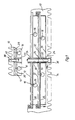
- Printed circuit boards 12 are held at their edges in a housing 10.
- the housing 10 consists of a good heat-conducting metal and is provided with cooling fins 14.
- the printed circuit boards 12 carry electrical components 16 on one side (bottom in FIG. 1).
- the components 16 extend in a conventional manner with connecting wires 18 through the printed circuit boards 12 and are on the other side (top side in FIG. 1) (solder side) soldered to conductor tracks.
- the printed circuit boards 12 carry a highly thermally conductive layer 20.
- the thermally conductive layer 20 is a heat-conducting sheet which is attached to the printed circuit board 12.
- the heat-conducting layer 20 is in additional heat-conducting contact with the housing 10 via a heat-conducting block 22, which is provided in a central region of the printed circuit board 12.
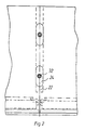
- the heat-conducting block 22 is a metal strip which is provided on the side of the heat-conducting layer 20 and is in heat-conducting contact therewith and extends across the printed circuit board 12.
- the metal strip lugs 24 are provided which extend through the heat-conducting layer 20 and the printed circuit board 12. As can be seen from Fig. 2, in the preferred embodiment, the lugs 24 are elongated, extending along the metal bar.
- a plurality of circuit boards 12 are arranged parallel to one another and at a distance from one another.
- the heat-conducting block 22 of each printed circuit board 12 bears on the inner wall 26 of the housing 10 or on the lugs 24 of the heat-conducting block 22 of the adjacent printed circuit board 12, as shown in FIG. 1 for the upper of the two printed circuit boards 12 shown.
- the circuit boards 12 are arranged between and parallel to opposite inner walls 26 and 28 of the housing 10.
- the end plate on one side (the lowermost printed circuit board 12 in FIG. 1) lies with the heat-conducting block 22 on an inner wall 26 of the housing 10.
- the end plate on the other side (the uppermost printed circuit board 12 in FIG.
- the heat dissipation blocks 22 are preferably made of aluminum.
Landscapes
- Engineering & Computer Science (AREA)
- Microelectronics & Electronic Packaging (AREA)
- Physics & Mathematics (AREA)
- Thermal Sciences (AREA)
- Aviation & Aerospace Engineering (AREA)
- Cooling Or The Like Of Electrical Apparatus (AREA)
Claims (6)
Applications Claiming Priority (2)
| Application Number | Priority Date | Filing Date | Title |
|---|---|---|---|
| DE3331112 | 1983-08-30 | ||
| DE19833331112 DE3331112A1 (de) | 1983-08-30 | 1983-08-30 | Vorrichtung zur waermeabfuhr von leiterplatten |
Publications (2)
| Publication Number | Publication Date |
|---|---|
| EP0136454A1 EP0136454A1 (fr) | 1985-04-10 |
| EP0136454B1 true EP0136454B1 (fr) | 1987-05-13 |
Family
ID=6207712
Family Applications (1)
| Application Number | Title | Priority Date | Filing Date |
|---|---|---|---|
| EP84108975A Expired EP0136454B1 (fr) | 1983-08-30 | 1984-07-28 | Dispositif pour la dissipation de chaleur des plaquettes à circuit imprimé |
Country Status (3)
| Country | Link |
|---|---|
| US (1) | US4583149A (fr) |
| EP (1) | EP0136454B1 (fr) |
| DE (2) | DE3331112A1 (fr) |
Families Citing this family (13)
| Publication number | Priority date | Publication date | Assignee | Title |
|---|---|---|---|---|
| DE3536963A1 (de) * | 1985-10-17 | 1987-04-23 | Diehl Gmbh & Co | Baugruppenanordnung |
| DE3813364A1 (de) * | 1988-04-21 | 1989-11-02 | Bodenseewerk Geraetetech | Vorrichtung zur waermeabfuhr von bauelementen auf einer leiterplatte |
| US5329420A (en) * | 1990-02-28 | 1994-07-12 | Altoz Frank E | Slotted tuning fork thermal interface |
| GB2259408A (en) * | 1991-09-07 | 1993-03-10 | Motorola Israel Ltd | A heat dissipation device |
| DE4310446C1 (de) * | 1993-03-31 | 1994-05-05 | Export Contor Ausenhandelsgese | Schaltungsanordnung |
| WO1996013048A1 (fr) * | 1994-10-19 | 1996-05-02 | Philips Electronics N.V. | Lampe electrique |
| US5506751A (en) * | 1994-10-26 | 1996-04-09 | Chatel; Louis R. | Extruded card cage |
| US6086404A (en) * | 1998-07-02 | 2000-07-11 | Advanced Processing Laboratories, Inc. | Circuit board card cage with one-piece integral card guide units |
| US5986887A (en) * | 1998-10-28 | 1999-11-16 | Unisys Corporation | Stacked circuit board assembly adapted for heat dissipation |
| FR2821497B1 (fr) * | 2001-02-27 | 2004-07-16 | Bosch Gmbh Robert | Entrainement electrique notamment entrainement d'essuie-glaces |
| US7046520B2 (en) * | 2003-04-07 | 2006-05-16 | Honeywell International, Inc. | Electronic assemblies having supports for circuit boards |
| DE102008033193A1 (de) | 2008-07-15 | 2010-02-04 | Continental Automotive Gmbh | Motorsteuerungsvorrichtung eines Fahrzeugs |
| DE102019218263A1 (de) * | 2019-11-26 | 2021-05-27 | Robert Bosch Gmbh | Leiterplatinenanordnung, insbesondere für eine Steuerelektronik einer elektromo-torischen Antriebseinheit, mit einem ersten und einem zweiten Leiterplatinenabschnitt |
Citations (4)
| Publication number | Priority date | Publication date | Assignee | Title |
|---|---|---|---|---|
| DE1243252B (de) * | 1965-05-17 | 1967-06-29 | Int Standard Electric Corp | Gehaeuse zur Aufnahme gedruckter Schaltungsplatten, das allseitig geschlossen aus Blechteilen hergestellt ist |
| US3631325A (en) * | 1970-06-15 | 1971-12-28 | Sperry Rand Corp | Card module and end wall treatment facilitating heat transfer and sliding |
| DE2744341A1 (de) * | 1977-10-01 | 1979-04-12 | Teldix Gmbh | Vorrichtung zur aufnahme von elektronik-leiterplatten |
| DE8221756U1 (de) * | 1982-07-30 | 1982-11-04 | Siemens AG, 1000 Berlin und 8000 München | Einrichtung zur Wärmeableitung von thermisch belasteten flächigen Bauelementen der Nachrichtentechnik |
Family Cites Families (6)
| Publication number | Priority date | Publication date | Assignee | Title |
|---|---|---|---|---|
| US3487267A (en) * | 1968-01-02 | 1969-12-30 | Jerrold Electronics Corp | Thermally conducting transistor support arms |
| DE2336168B1 (de) * | 1973-07-16 | 1974-10-03 | Siemens Ag | Horizontal-Ablenk-Baustein |
| FR2413016A1 (fr) * | 1977-12-26 | 1979-07-20 | Radiotechnique Compelec | Circuits imprimes multicouches a collecteur thermique incorpore |
| DE7740059U1 (de) * | 1977-12-29 | 1980-04-03 | Neumann Elektronik Gmbh, 4330 Muelheim | Befestigungsvorrichtung zur elektrisch isolierten Befestigung von Bauelementen, die eine erhebliche Verlustwärme erzeugen |
| US4386390A (en) * | 1981-01-21 | 1983-05-31 | The Bendix Corporation | Vibration adjustable spacer |
| US4475145A (en) * | 1982-07-12 | 1984-10-02 | Rockwell International Corporation | Circuit board heatsink assembly and technique |
-
1983
- 1983-08-30 DE DE19833331112 patent/DE3331112A1/de not_active Withdrawn
-
1984
- 1984-07-28 EP EP84108975A patent/EP0136454B1/fr not_active Expired
- 1984-07-28 DE DE8484108975T patent/DE3463719D1/de not_active Expired
- 1984-08-13 US US06/639,833 patent/US4583149A/en not_active Expired - Fee Related
Patent Citations (4)
| Publication number | Priority date | Publication date | Assignee | Title |
|---|---|---|---|---|
| DE1243252B (de) * | 1965-05-17 | 1967-06-29 | Int Standard Electric Corp | Gehaeuse zur Aufnahme gedruckter Schaltungsplatten, das allseitig geschlossen aus Blechteilen hergestellt ist |
| US3631325A (en) * | 1970-06-15 | 1971-12-28 | Sperry Rand Corp | Card module and end wall treatment facilitating heat transfer and sliding |
| DE2744341A1 (de) * | 1977-10-01 | 1979-04-12 | Teldix Gmbh | Vorrichtung zur aufnahme von elektronik-leiterplatten |
| DE8221756U1 (de) * | 1982-07-30 | 1982-11-04 | Siemens AG, 1000 Berlin und 8000 München | Einrichtung zur Wärmeableitung von thermisch belasteten flächigen Bauelementen der Nachrichtentechnik |
Also Published As
| Publication number | Publication date |
|---|---|
| DE3331112A1 (de) | 1985-03-14 |
| US4583149A (en) | 1986-04-15 |
| EP0136454A1 (fr) | 1985-04-10 |
| DE3463719D1 (en) | 1987-06-19 |
Similar Documents
| Publication | Publication Date | Title |
|---|---|---|
| EP0920055B1 (fr) | Dispositif de refroidissement pour un composant générant de la chaleur sur un circuit imprimé | |
| DE69400105T2 (de) | Befestigungsteil mit geneigter Spiralfeder für Wärmesenke für ein elektronisches Bauelement | |
| DE112008000452B4 (de) | Halbleitermodul und Wechselrichtervorrichtung | |
| DE69401137T2 (de) | Kühlungsanordnung für elektrische Leistungsbauteile | |
| DE69637488T2 (de) | Halbleiter und Halbleitermodul | |
| WO1994029901A1 (fr) | Dispositif de fixation pour elements semi-conducteurs de circuit | |
| DE4335946C2 (de) | Anordnung bestehend aus einer Leiterplatte | |
| DE102021132148A1 (de) | Leiterplattenanordnung | |
| DE4027072A1 (de) | Halbleiteranordnung | |
| EP0278240A2 (fr) | Radiateur, en particulier pour le refroidissement de composants électroniques | |
| EP1445799A2 (fr) | Dispositif à dissipation de chaleur pour un semi-conducteur sur un circuit imprimé | |
| DE202019105232U1 (de) | Gespleißte mehrschichtige Leiterplatte | |
| EP0136454A1 (fr) | Dispositif pour la dissipation de chaleur des plaquettes à circuit imprimé | |
| DE3784247T2 (de) | Halbleiter-zusammenbau. | |
| DE4226816C2 (de) | Vorrichtung zur Wärmeableitung aus einem Gehäuse einer integrierten Schaltung | |
| DE3237878C2 (de) | Anordnung zur Abführung der Verlustwärme eines auf einer Leiterplatte montierten Halbleiterbauelementes | |
| DE3614086C2 (de) | Vorrichtung zur Wärmeableitung von einer elektronische Komponenten enthaltenden Baueinheit und Verfahren zum thermischen Koppeln einer elektronische Komponenten enthaltenden Baueinheit | |
| EP0652694B1 (fr) | Appareil de commande pour automobile | |
| EP0180730B1 (fr) | Agencement pour la compensation de tension et pour la dissipation de la chaleur d'un composant électronique | |
| EP0113794A1 (fr) | Support pour des plaquettes de composants | |
| EP1393375B1 (fr) | Systeme de contact | |
| DE3628556C1 (en) | Semiconductor device | |
| DE112014004097B4 (de) | Halbleitervorrichtung | |
| EP4033867B1 (fr) | Dispositif de commutation électrique | |
| DE3437774C2 (fr) |
Legal Events
| Date | Code | Title | Description |
|---|---|---|---|
| PUAI | Public reference made under article 153(3) epc to a published international application that has entered the european phase |
Free format text: ORIGINAL CODE: 0009012 |
|
| AK | Designated contracting states |
Designated state(s): DE FR GB |
|
| 17P | Request for examination filed |
Effective date: 19850306 |
|
| RTI1 | Title (correction) | ||
| 17Q | First examination report despatched |
Effective date: 19860923 |
|
| GRAA | (expected) grant |
Free format text: ORIGINAL CODE: 0009210 |
|
| AK | Designated contracting states |
Kind code of ref document: B1 Designated state(s): DE FR GB |
|
| REF | Corresponds to: |
Ref document number: 3463719 Country of ref document: DE Date of ref document: 19870619 |
|
| ET | Fr: translation filed | ||
| PLBE | No opposition filed within time limit |
Free format text: ORIGINAL CODE: 0009261 |
|
| STAA | Information on the status of an ep patent application or granted ep patent |
Free format text: STATUS: NO OPPOSITION FILED WITHIN TIME LIMIT |
|
| 26N | No opposition filed | ||
| PGFP | Annual fee paid to national office [announced via postgrant information from national office to epo] |
Ref country code: FR Payment date: 19980604 Year of fee payment: 15 |
|
| PGFP | Annual fee paid to national office [announced via postgrant information from national office to epo] |
Ref country code: GB Payment date: 19980716 Year of fee payment: 15 |
|
| PGFP | Annual fee paid to national office [announced via postgrant information from national office to epo] |
Ref country code: DE Payment date: 19980922 Year of fee payment: 15 |
|
| PG25 | Lapsed in a contracting state [announced via postgrant information from national office to epo] |
Ref country code: GB Free format text: LAPSE BECAUSE OF NON-PAYMENT OF DUE FEES Effective date: 19990728 |
|
| PG25 | Lapsed in a contracting state [announced via postgrant information from national office to epo] |
Ref country code: FR Free format text: THE PATENT HAS BEEN ANNULLED BY A DECISION OF A NATIONAL AUTHORITY Effective date: 19990731 |
|
| GBPC | Gb: european patent ceased through non-payment of renewal fee |
Effective date: 19990728 |
|
| PG25 | Lapsed in a contracting state [announced via postgrant information from national office to epo] |
Ref country code: DE Free format text: LAPSE BECAUSE OF NON-PAYMENT OF DUE FEES Effective date: 20000503 |
|
| REG | Reference to a national code |
Ref country code: FR Ref legal event code: ST |