EP0136672B1 - Procédé et appareil pour l'exposition aux rayons X - Google Patents
Procédé et appareil pour l'exposition aux rayons X Download PDFInfo
- Publication number
- EP0136672B1 EP0136672B1 EP84111626A EP84111626A EP0136672B1 EP 0136672 B1 EP0136672 B1 EP 0136672B1 EP 84111626 A EP84111626 A EP 84111626A EP 84111626 A EP84111626 A EP 84111626A EP 0136672 B1 EP0136672 B1 EP 0136672B1
- Authority
- EP
- European Patent Office
- Prior art keywords
- ray
- mask
- stop
- ray exposure
- exposure
- Prior art date
- Legal status (The legal status is an assumption and is not a legal conclusion. Google has not performed a legal analysis and makes no representation as to the accuracy of the status listed.)
- Expired
Links
Images





Classifications
-
- G—PHYSICS
- G03—PHOTOGRAPHY; CINEMATOGRAPHY; ANALOGOUS TECHNIQUES USING WAVES OTHER THAN OPTICAL WAVES; ELECTROGRAPHY; HOLOGRAPHY
- G03F—PHOTOMECHANICAL PRODUCTION OF TEXTURED OR PATTERNED SURFACES, e.g. FOR PRINTING, FOR PROCESSING OF SEMICONDUCTOR DEVICES; MATERIALS THEREFOR; ORIGINALS THEREFOR; APPARATUS SPECIALLY ADAPTED THEREFOR
- G03F7/00—Photomechanical, e.g. photolithographic, production of textured or patterned surfaces, e.g. printing surfaces; Materials therefor, e.g. comprising photoresists; Apparatus specially adapted therefor
- G03F7/70—Microphotolithographic exposure; Apparatus therefor
- G03F7/70058—Mask illumination systems
-
- H—ELECTRICITY
- H10—SEMICONDUCTOR DEVICES; ELECTRIC SOLID-STATE DEVICES NOT OTHERWISE PROVIDED FOR
- H10D—INORGANIC ELECTRIC SEMICONDUCTOR DEVICES
- H10D99/00—Subject matter not provided for in other groups of this subclass
-
- G—PHYSICS
- G03—PHOTOGRAPHY; CINEMATOGRAPHY; ANALOGOUS TECHNIQUES USING WAVES OTHER THAN OPTICAL WAVES; ELECTROGRAPHY; HOLOGRAPHY
- G03F—PHOTOMECHANICAL PRODUCTION OF TEXTURED OR PATTERNED SURFACES, e.g. FOR PRINTING, FOR PROCESSING OF SEMICONDUCTOR DEVICES; MATERIALS THEREFOR; ORIGINALS THEREFOR; APPARATUS SPECIALLY ADAPTED THEREFOR
- G03F7/00—Photomechanical, e.g. photolithographic, production of textured or patterned surfaces, e.g. printing surfaces; Materials therefor, e.g. comprising photoresists; Apparatus specially adapted therefor
- G03F7/20—Exposure; Apparatus therefor
- G03F7/2037—Exposure with X-ray radiation or corpuscular radiation, through a mask with a pattern opaque to that radiation
- G03F7/2039—X-ray radiation
-
- H—ELECTRICITY
- H10—SEMICONDUCTOR DEVICES; ELECTRIC SOLID-STATE DEVICES NOT OTHERWISE PROVIDED FOR
- H10P—GENERIC PROCESSES OR APPARATUS FOR THE MANUFACTURE OR TREATMENT OF DEVICES COVERED BY CLASS H10
- H10P95/00—Generic processes or apparatus for manufacture or treatments not covered by the other groups of this subclass
Definitions
- the present invention relates to a method and an apparatus for X-ray exposure to transfer a pattern shape formed on a mask onto a photoresist layer applied to the surface of a wafer.
- Such as integrated circuits (IC) or large scale integrated circuits (LSI) are so manufactured in order to obtain desired circuits as by forming a photoresist layer covering the surface of a wafer made of silicon, transferring a desired pattern formed on a mask onto the photoresist layer, and performing repetitive processing such as etching, ion-implantation or the like in accordance with the transferred pattern.
- IC integrated circuits
- LSI large scale integrated circuits
- Fig. 1 shows an outline of a prior art of step-and-repeat type X-ray exposure apparatus.
- X-rays 2 from an X-ray source 1 are irradiated on a mask 3, and a pattern 4 on the mask 3 is transferred onto a photoresist on a wafer 5.
- a precise transferring with a sub-micron electric passage width an exposure onto the surface of the wafer 5 is successively carried out by step-and-repeat in which by an exposure area at one time is taken in a small area.
- One of the reasons for this is to improve the precision of dimension.
- a short wavelength X-ray (called as a hard X-ray) for medical care is not used for the X-ray source 1, but a low permeability and long wavelength X-ray (called as a soft X-ray) is used for the X-ray source 1 for some reasons associated with the material of the mask described later. More specifically, such as M o ⁇ L o rays 5.4 A or the like, having a wavelength of several A to several tens A, are used. Soft X-rays are selectively used among white X-rays, such as obtained from the SOR (Synchrotron Orbital Radiation).
- the mask 3 comprises a supporting ring 7 (for example, made of silicon), a back ring 8 for reinforcing the supporting ring (for example, made of a plate glass), a membrane 9 (for example, made of organic material or inorganic material such as BN, Si 3 N 4 or the like) applied to and extended along the supporting ring 7 for serving as an X-ray permeable member, and a pattern section 10 (such as having 0.8 pm thickness of gold) for patterning by intercepting the X-rays.
- a supporting ring 7 for example, made of silicon
- a back ring 8 for reinforcing the supporting ring
- a membrane 9 for example, made of organic material or inorganic material such as BN, Si 3 N 4 or the like
- a pattern section 10 such as having 0.8 pm thickness of gold
- the contrast C is the X-ray exposure is hard to obtain a larger contrast regardless of an appropriate selection of the wavelength, due to the fact that X-rays are stronger in transmission than visual light rays.
- An X-ray transmission coefficient K of an object irradiated by X-rays is expressed in the following formula.
- Kp a transmission coefficient of the pattern section
- K t an X-raytransmission coefficient of the transmission section.
- the area A2 is not exposed with a pattern of an adjacent exposure area, but is irradiated with X-rays transmitted through a thin gold layer of an adjacent exposure area so that the contrast is worsened.
- the contrasts C 2 and C 3 for the areas A2 and A3 respectively are:
- the contrasting C N for the N-multiple exposure is represented by:
- the contrast C 1 in the formula (4) is, for example, 10
- the contrasts C 2 and C 3 are largely deteriorated 5.5 and 4 respectively. Therefore, in the case all the areas A1, A2, and A3 are exposed, material should be chosen in correspondence with the area A3 having the smallest contrast.
- the thickness of gold of the pattern section 10 is required to have for example 1 pm. Assuming that the width of a wiring line is 0.5 pm, it is necessary to realize a pattern with an aspect ratio of 2, which is extraordinary hard to manufacture. Further, the difference of contrasts among the areas A1, A2, and A3 becomes large so that the controllability for the width of transferred pattern becomes worse, which results in a great hardness for the control of a wiring line width such as 0.5 pm ⁇ 0.1 um.
- the present invention has been made in view of the above circumstances, and it is an object to provide a method for X-ray exposure and an exposure apparatus suitable for practicing the method as above, in which the X-ray exposure for the area other than the required area is intercepted for every shot so that there is no fear of making the contrasts of adjacent areas worsen.
- a further object is to provide an improved apparatus for X-ray exposure which is adaptive to changing of a mask pattern or shot area, while contrast characteristic is improved.
- Fig. 1 is a perspective view simplified X-ray exposure apparatus for explaining the X-ray exposure
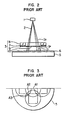
- Fig. 2 is a vertical sectional view of a prior art X-ray exposure to apparatus
- Fig. 3 is a plan view showing the top surface of a wafer in the X-ray exposure apparatus of Fig. 2
- Fig. 4 is a vertical section showing one embodiment according to the present invention
- Fig. 5 is a plan view showing the top surface of a wafer in the above embodiment of Fig. 4
- Fig. 6 is a diagram for explaining the position precision in the above embodiment of Fig. 4
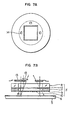
- Figs. 7 are concrete arrangements of masks in the above embodiment of Fig. 4, wherein Fig. 7A is a plan view and Fig. 7B is a vertical section.
- Figs. 8 through 10 are vertical sections of masks different from the above embodiment
- Fig. 11 is a plan view showing a top surface of a stop according to further embodiment of the invention
- Fig. 12 is a plan view showing a top surface of a stop according to further embodiment of the invention
- Fig. 13 is a partial plan view of the stop according to the other embodiment of the invention.
- Fig. 4 is a diagram conceptually showing a stop means for intercepting surplus X-rays in accordance with the present invention
- Fig. 5 is a view for illustrating the operation of the stop means.
- the stop 11 is made of a material not allowing the transmission of X-rays (more in detail, by using a material with a low transmission coefficient for X-rays, having such a thickness that makes it possible to consider the transmission amount of X-rays as substantially zero in a practical use), and is constructed to have a configuration (described later in detail) covering the area other than the exposure area Ex.
- the intensity I B of an X-ray passing the stop 11 is:
- K B is an X-ray transmission coefficient of the stop 11.
- the contrast C N ' for the area subjecting to N-multiple exposures is generally represented by: which shows that the contrast for such an area is large when compared with that represented by the formula (7) indicative of the contrast in the prior art.
- the material quality and thickness of the stop 11 are selected in compliance with the following procedure and criterion: (1) N is determined by the maximum number of mutiple exposures in the step-and-repeat process. (2) the contrast and contrast precision necessary for transferring the pattern section 10 are determined and represented as Cp ⁇ ACp. (3) the above determinations along with the formulas (12) and (9), give the following: and I b is determined so as to suffice the formulas (13) and (14), then the transmission coefficient is determined from the formula (8), and the material quality and thickness are derived from the formula (1).
- a penumbra Bp of the pattern section 10 is existed on the photoresist 6 by the X-ray source 1 with a dimension of d.
- the stop 11 as well produces a penumbra B B as shown in the figure: where M: a distance between the stop 11 and the pattern section.
- the penumbra B is a distance between the adjacent shots 12 (refer to Fig. 5), and it is commonly a scribe area (about 50 to 100 pm). If an allowance value for the penumbra B B , a penumbra Bp, an X-ray source diameter d, and gap G are determined, then, by using the formulas (15) and (16), the distance of the stop 11 from the pattern section 10 is determined. Further, the precision for determining the position of the stop 11 in horizontal direction with respect to the mask surface may be determined by the space between adjacent shots in consideration of the penumbra B B , such that the tolerances of the stop position and penumbra B B are included within the space of shots.
- FIG. 7A A concrete plan view of the mask 3' in the above embodiment is shown in Fig. 7A, and the similar front section is shown in Fig. 7B.
- a stop 11 made of aluminum plate of 1 mm * is bonded between the supporting ring 7 and the back ring 8.
- the inner edge surface cut out of the aluminum plate are machined in accordance with the radiation angle 13 of the X-ray 2.
- flatness of the machined inner edge surface of stop 11 is finished within about ⁇ 1 pm.
- an alignment aperture 14 is provided for enabling an alignment.
- a shutter 15 may be mounted at the side of the X-ray source. The construction and position of the shutter 15 are determined similarly to the stop 11.
- the shutter 15 is of such an arrangement that when the alignment is carried out it is opened and when the exposure is carried out it is closed.
- the working for the edge surface of the stop 11 made of aluminum can be dispensed with sometimes depending upon the precision for determining the position of the penumbra B B or the like.
- either one of the upper and lower stops 18a and 18b may be omitted. Also, it may be possible to additionally employ each stop means respectively described in the above embodiments.
- Fig. 11 shows only a stop apparatus which is formed by two separated movable plates 110.
- the movable plates 110 can be slided in the horizontal direction of arrows X and Y manually or by a driving device, so that the opening shape or area can be varied at one's desire. Therefore in this embodiment, the X-ray exposure apparatus can adaptive to various shapes of the patterns without deteriorating contrast characteristic, and can also expose only a particular portion of wafer.
- the opening of the stop 11 is fixed.
- another plate 111 which is un-permeable to X-ray covers the opening.
- the shape and area of the opening can be controlled by sliding the plate 111 so as to obtain same effects as shown in the embodiment of Fig. 11.
- the opening is covered by a layer of which material is permeable to X-ray.
- Another plate 112 which is non- permeable to X-ray is disposed on the opening layer. Therefore, X-ray can be passed only an area than the plate 112 in the opening of the stop 11.
- An area of the exposing shot can be controlled according to the shape and position of the plate 112.
- stop 11 can be rotated in a horizontal plane so as to change shot area of the wafer.
Landscapes
- Physics & Mathematics (AREA)
- General Physics & Mathematics (AREA)
- Health & Medical Sciences (AREA)
- Toxicology (AREA)
- Exposure Of Semiconductors, Excluding Electron Or Ion Beam Exposure (AREA)
- Exposure And Positioning Against Photoresist Photosensitive Materials (AREA)
Claims (7)
- (1)
Applications Claiming Priority (2)
| Application Number | Priority Date | Filing Date | Title |
|---|---|---|---|
| JP58180684A JPH0715869B2 (ja) | 1983-09-30 | 1983-09-30 | 軟x線露光装置 |
| JP180684/83 | 1983-09-30 |
Publications (3)
| Publication Number | Publication Date |
|---|---|
| EP0136672A2 EP0136672A2 (fr) | 1985-04-10 |
| EP0136672A3 EP0136672A3 (en) | 1987-05-13 |
| EP0136672B1 true EP0136672B1 (fr) | 1990-12-19 |
Family
ID=16087494
Family Applications (1)
| Application Number | Title | Priority Date | Filing Date |
|---|---|---|---|
| EP84111626A Expired EP0136672B1 (fr) | 1983-09-30 | 1984-09-28 | Procédé et appareil pour l'exposition aux rayons X |
Country Status (4)
| Country | Link |
|---|---|
| EP (1) | EP0136672B1 (fr) |
| JP (1) | JPH0715869B2 (fr) |
| KR (1) | KR850002692A (fr) |
| DE (1) | DE3483762D1 (fr) |
Families Citing this family (4)
| Publication number | Priority date | Publication date | Assignee | Title |
|---|---|---|---|---|
| DE68922945T2 (de) * | 1988-09-09 | 1995-11-16 | Canon K.K., Tokio/Tokyo | Belichtungsvorrichtung. |
| JP2805220B2 (ja) * | 1989-09-21 | 1998-09-30 | キヤノン株式会社 | 露光装置 |
| JP2860578B2 (ja) * | 1990-03-02 | 1999-02-24 | キヤノン株式会社 | 露光装置 |
| DE69128655T2 (de) * | 1990-03-02 | 1998-05-07 | Canon K.K., Tokio/Tokyo | Belichtungsgerät |
Family Cites Families (2)
| Publication number | Priority date | Publication date | Assignee | Title |
|---|---|---|---|---|
| JPS55129333A (en) * | 1979-03-28 | 1980-10-07 | Hitachi Ltd | Scale-down projection aligner and mask used for this |
| JPS55132039A (en) * | 1979-04-02 | 1980-10-14 | Mitsubishi Electric Corp | Forming method for repeated figure |
-
1983
- 1983-09-30 JP JP58180684A patent/JPH0715869B2/ja not_active Expired - Lifetime
-
1984
- 1984-09-28 EP EP84111626A patent/EP0136672B1/fr not_active Expired
- 1984-09-28 DE DE8484111626T patent/DE3483762D1/de not_active Expired - Lifetime
- 1984-09-28 KR KR1019840006002A patent/KR850002692A/ko not_active Ceased
Also Published As
| Publication number | Publication date |
|---|---|
| DE3483762D1 (de) | 1991-01-31 |
| EP0136672A2 (fr) | 1985-04-10 |
| JPH0715869B2 (ja) | 1995-02-22 |
| EP0136672A3 (en) | 1987-05-13 |
| KR850002692A (ko) | 1985-05-15 |
| JPS6074518A (ja) | 1985-04-26 |
Similar Documents
| Publication | Publication Date | Title |
|---|---|---|
| KR100517678B1 (ko) | 포토리소그래피 시스템에서 렌즈 에러를 보상하는 레티클 | |
| EP0444937B1 (fr) | Appareil de pose | |
| JP2860578B2 (ja) | 露光装置 | |
| JP3291408B2 (ja) | 露光装置および集積回路の製造方法 | |
| US5291239A (en) | System and method for leveling semiconductor wafers | |
| US7521697B2 (en) | Method for fabricating semiconductor device and equipment for fabricating the same | |
| US6642528B2 (en) | Alignment mark detection method, and alignment method, exposure method and device, and device production method, making use of the alignment mark detection method | |
| EP0136672B1 (fr) | Procédé et appareil pour l'exposition aux rayons X | |
| JP2697014B2 (ja) | 露光装置及び露光方法 | |
| US4349621A (en) | Process for X-ray microlithography using thin film eutectic masks | |
| JPH03108310A (ja) | 露光装置 | |
| EP0531066B1 (fr) | Système d'exposition pour synchrotron et méthode de fabrication de dispositifs semi-conducteurs utilisant ce système | |
| US5793472A (en) | Exposure method using reference marks on both the mask and the substrate and capable of providing high alignment precision even after multiple exposures | |
| US6791668B2 (en) | Semiconductor manufacturing apparatus and method | |
| JP3082747B2 (ja) | 露光装置の評価方法 | |
| JPH03235321A (ja) | X線露光用マスク | |
| Cullmann et al. | Experimental results with a scanning stepper for synchrotron‐based x‐ray lithography | |
| JPH0713565B2 (ja) | マスク位置合わせ方法 | |
| JP2001267235A (ja) | 露光装置及びその露光装置におけるフォトマスクの位置合わせ方法 | |
| JPH0527413A (ja) | 露光装置用ホトマスク | |
| JP2644570B2 (ja) | X線露光装置及び素子製造方法 | |
| JP3284299B2 (ja) | ブラインド装置 | |
| JPS61172328A (ja) | X線露光方法およびその装置 | |
| JPS62144325A (ja) | 目合せ位置決め方法 | |
| Di Fabrizio et al. | A novel X-ray mask concept for mex&match lithography fabrication of MOS devices by synchrotron radiation lithography |
Legal Events
| Date | Code | Title | Description |
|---|---|---|---|
| PUAI | Public reference made under article 153(3) epc to a published international application that has entered the european phase |
Free format text: ORIGINAL CODE: 0009012 |
|
| 17P | Request for examination filed |
Effective date: 19840928 |
|
| AK | Designated contracting states |
Designated state(s): DE FR GB |
|
| PUAL | Search report despatched |
Free format text: ORIGINAL CODE: 0009013 |
|
| AK | Designated contracting states |
Kind code of ref document: A3 Designated state(s): DE FR GB |
|
| 17Q | First examination report despatched |
Effective date: 19890619 |
|
| GRAA | (expected) grant |
Free format text: ORIGINAL CODE: 0009210 |
|
| AK | Designated contracting states |
Kind code of ref document: B1 Designated state(s): DE FR GB |
|
| REF | Corresponds to: |
Ref document number: 3483762 Country of ref document: DE Date of ref document: 19910131 |
|
| ET | Fr: translation filed | ||
| PLBE | No opposition filed within time limit |
Free format text: ORIGINAL CODE: 0009261 |
|
| STAA | Information on the status of an ep patent application or granted ep patent |
Free format text: STATUS: NO OPPOSITION FILED WITHIN TIME LIMIT |
|
| 26N | No opposition filed | ||
| PGFP | Annual fee paid to national office [announced via postgrant information from national office to epo] |
Ref country code: GB Payment date: 19920918 Year of fee payment: 9 |
|
| PG25 | Lapsed in a contracting state [announced via postgrant information from national office to epo] |
Ref country code: GB Effective date: 19930928 |
|
| GBPC | Gb: european patent ceased through non-payment of renewal fee |
Effective date: 19930928 |
|
| PGFP | Annual fee paid to national office [announced via postgrant information from national office to epo] |
Ref country code: FR Payment date: 19960716 Year of fee payment: 13 |
|
| PG25 | Lapsed in a contracting state [announced via postgrant information from national office to epo] |
Ref country code: FR Free format text: THE PATENT HAS BEEN ANNULLED BY A DECISION OF A NATIONAL AUTHORITY Effective date: 19970930 |
|
| REG | Reference to a national code |
Ref country code: FR Ref legal event code: ST |
|
| PGFP | Annual fee paid to national office [announced via postgrant information from national office to epo] |
Ref country code: DE Payment date: 19981028 Year of fee payment: 15 |
|
| PG25 | Lapsed in a contracting state [announced via postgrant information from national office to epo] |
Ref country code: DE Free format text: LAPSE BECAUSE OF NON-PAYMENT OF DUE FEES Effective date: 20000701 |