EP0136677B1 - Récepteur d'appel multifonctions susceptible de réduire le nombre de touches - Google Patents
Récepteur d'appel multifonctions susceptible de réduire le nombre de touches Download PDFInfo
- Publication number
- EP0136677B1 EP0136677B1 EP84111639A EP84111639A EP0136677B1 EP 0136677 B1 EP0136677 B1 EP 0136677B1 EP 84111639 A EP84111639 A EP 84111639A EP 84111639 A EP84111639 A EP 84111639A EP 0136677 B1 EP0136677 B1 EP 0136677B1
- Authority
- EP
- European Patent Office
- Prior art keywords
- signal
- message
- manual
- mode
- modes
- Prior art date
- Legal status (The legal status is an assumption and is not a legal conclusion. Google has not performed a legal analysis and makes no representation as to the accuracy of the status listed.)
- Expired
Links
Images


Classifications
-
- H—ELECTRICITY
- H04—ELECTRIC COMMUNICATION TECHNIQUE
- H04W—WIRELESS COMMUNICATION NETWORKS
- H04W8/00—Network data management
- H04W8/22—Processing or transfer of terminal data, e.g. status or physical capabilities
- H04W8/24—Transfer of terminal data
- H04W8/245—Transfer of terminal data from a network towards a terminal
-
- H—ELECTRICITY
- H04—ELECTRIC COMMUNICATION TECHNIQUE
- H04W—WIRELESS COMMUNICATION NETWORKS
- H04W88/00—Devices specially adapted for wireless communication networks, e.g. terminals, base stations or access point devices
- H04W88/02—Terminal devices
- H04W88/022—Selective call receivers
Definitions
- a recent technical development have brought about a multifunctional pager receiver which can provide not only an indication of a terminating call but also visual displays of messages on a display unit.
- a storage unit is installed in such a pager receiver so as to store the messages.
- a storage capacity of the memory unit tends to increase to satisfy a recent demand.
- WO 83/01357 describes a pager receiver with a visual display, means for identifying a desired recipient of signal on the receiver, means for storing a received signal, means for displaying the number of messages received and means for displaying a plurality of messages received.
- a conventional pager receiver of the type described comprises a plurality of manual switches for the different manual modes.
- the pager receiver With an increase of the manual switches, the pager receiver inevitably becomes bulky in size. Accordingly, portability of the pager receiver becomes worse with the increase of manual switches. Operation errors may occur frequently when the manual switches increase in number.
- a pager receiver 21 is operable in response to a radio call signal which is transmitted from a transmitting station 22.
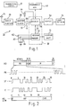
- the radio call signal RD comprises a preamble signal PR of 62 bits, a frame synchronization signal SC of 31 bits, a call number signal AD of 31 bits, a message signal M, and an end signal E of 31 bits, which are all successively arranged to form a frame, as depicted along a top line.
- the preamble signal PR is specified by a repetition of pulses equal in number to 62, as shown along a second line labelled PR.
- the frame synchronization signal SC has a fixed pattern of 31 bits, as illustrated along a third line labelled SC.
- each frame is variable in length depending on the number of the message signals.
- the message signal M have a bit rate different from that of the call number signal AD. It is assumed that the bit rates of the message and the call number signals M and AD are equal, for example, to 200 and 100 Hz, respectively.
- the radio call signal is sent through an antenna 24 to a radio portion 26 to be subjected to amplication, frequency conversion, and the like in a well-known manner to be converted into a baseband signal BB carrying the preamble signal PR, the frame synchronization signal SC, the call number signal AD, the message signal M, and the end signal E, which are illustrated in Fig. 2.
- the baseband signal BB is supplied through a waveform shaper 28 to a processing circuit 30 as a succession of digital signals.
- the decoder 31 comprises a preamble signal detector 36 for detecting the preamble signal PR to produce a first detection signal DT, representative of detection of the preamble signal PR.
- a synchronization signal detector 37 and an end signal detector 38 detect the frame synchronization signal SC and the end signal E to produce second and third detection signals DT 2 and DT 3 representative of detection of the frame synchronization signal SC and the end signal E, respectively.
- Each of the preamble signal detector 36, the synchronization signal detector 37, and the end signal detector 38 can be consituted by a combination of a shift register, Exclusive OR gates and an AND gate.
- Bit synchronization and frame synchronization are established with reference to the baseband signal BB and the frame synchronization signal SC in a bit synchronization circuit (not shown) and the synchronization signal detector 37, respectively.
- a call number signal detector 39 detects the call number signal AD assigned to the pager receiver and produces a fourth detection signal DT 4 representative of detection of the call number signal AD.
- the fourth detection signal DT 4 is supplied through the decorder controller 41 to the message processor 32 and will simply be called a detection signal.
- the decoder controller 41 further comprises a driver circuit 49 connected to a first manual switch 51. Operation of the switch 51 will later be described in detail. For the time being, it may be mentioned that the driver circuit 49 supplies the message processor 32 with a first enable signal S, when the first manual switch 51 is closed by a possessor.
- a tone generating circuit 52 is controlled by the message processor 32 in a manner to be described and sends a tone signal TN to a loudspeaker 54 (Fig. 1) through a buffer circuit 56.
- the decoder controller 41 further comprises parts for producing the reset signal R and the like in a usual manner.
- the message processor 32 is put into operation in each manual mode in coopeation with a display unit 71.
- the manual modes are for manually accessing each message signal stored in the message processor 32 so as to display a message carried by the accessed message signal on the display unit 71, to erase the accessed message signal, or to preserve the accessed message signal.
- each message is displayed on the display unit 71 in the form of a succession of characters or letters. The succession is variable in length.
- the message processor 32 comprises a central processing unit (CPU) 75 which will be described later in detail in conjunction with Fig. 8, a random access memory (RAM) 76 storing each message signal, and a display driver circuit 78 for driving the driver unit 71 (Fig. 1).
- the remaining elements will be described in conjunction with Fig. 8.
- the random access memory 76 has a plurality of areas each of which is for storing a single one of the characters of each message and that each message occupies the areas determined by the length of the message. A total number of the areas is equal, for example, to 500. Messages stored in the random access memory 76 will be referred to as files or filed messages, respectively.
- the files may successiveively be sent to an external device, such as a printer, a microcomputer, or the like, through a predetermined terminal (not shown) of the message processor 32 under control of the central processing unit 75.
- an external device such as a printer, a microcomputer, or the like
- the display unit 71 can display only a preselected number of characters which is equal, for example, to 16. When a message consists of characters greater in number than the preselected number, the display unit 71 can not display a whole of the message in question at any time. In this event, the characters of the message may cyclically be displayed on the display unit 71. Such a display operation will be named a scroll operation.
- the central processing units 75 can carry out the scroll operation, as will become clear as the description proceeds.
- the message controller 32 is supplied with a source voltage V oo from a battery 81.
- the battery 81 is to be exchanged to another one some day.
- the files, namely, the filed messages may undesiredly be extinct from the random access memory 76.
- the illustrated message processor 32 comprises a diode 82 coupled to the battery 81 and a capacitor 83 connected to the diode 82 and the random access memory 76.
- the capacitance 83 is charged through the diode 82 by the battery 81 insofar as the battery 81 is not disconnected from the message processor 32.
- the filed messages are kept in the random access memory 76 by the source voltage V oo supplied from the battery 81.
- V oo supplied from the battery 81.
- the filed messages stored in the random access memory 76 are backed up by a combination of the diode 82 and the capacitor 83 which may be referred to as a backup circuit.
- control signals which may be present in the central processing unit 75 are transferred from the central processing unit 75 to the random access memory 76 during disconnection of the battery 81 when a backup operation is indicated by the possessor.
- the manual modes are divided into intermediate modes and final modes which succeed the intermediate modes and which are shown at the rightmost column of this figure.
- the intermediate modes are successively shifted to the final modes in accordance with the first through the fourth enable signals 5, to S 4 .
- the selection mode can be shifted to one of the final modes by production of the first enable signal S,.
- the first operation announcement indicates only the three intermediate modes without the one final mode in consideration of the number of characters which can be displayed on the display unit 71.
- the above-mentioned one final mode which is selected by closure of the first manual switch 51 may be indicated by a specification for the pager receiver.
- the second operation annoucement indicates three of the final modes.
- the final modes and the corrsponding operations are enumerated in Table 1.
- the second enable signal 5 2 is produced in the first intermediate mode by closure of the second manual switch 62.
- the message processor 75 is put into the readout display mode so as to display a specific one of the messages on the liquid crystal display member 85 (Fig. 7).
- the readout display mode is specified by a succession of production of the first enable signal S 1 and twice production of the second enable signal S 2 .
- the succession of the first and second enable signals S 1 and S 2 will be referred to as a third one of the mode signals.
- the second filed message be the specific one searched by the possessor.
- the first manual switch 51 is operated or closed by the possessor to produce the first enable signal S 1 while the second filed message is being displayed on the liquid crystal display member 85.
- the manual operation of the first manual switch 51 will be called a second manual operation and puts the message processor 32 into a second specific mode. In the second specific mode, the remaining parts of the specific message are successively displayed on the display unit 71.
- the message processor 32 is put into the second intermediate mode (Fig. 6) for announcing the file access operation and that the second manual switch 62 is operated as the first manual operation to produce the second enable signal S 2 . Consequently, the second intermediate mode is shifted to the preservation mode.
- the preservation mode is specified by a combination of the first, third, and second enable signals S i , 5 3 , and S 2 which may be called one of the mode signals.
- each leading part of the filed messages is successively read out of the random access memory 76 and displayed on the liquid crystal display member 85 in the manner described in conjunction with the readout display mode.
- the symbol P is luminous on the indicator member 86, as exemplified in Fig. 7(C), so as to specify the preservation mode. If the illustrated message "TODAY'S SCHEDULE" is to be preserved, the first manual switch 51 is operated as the second manual operation. As a result, the illustrated message is preserved without being erased from the random access memory 76.
- the memory backup mode is selected by closing the fourth manual switch 64 two times, as will readily be understood from Fig. 6.
- the central processing unit 75 (Fig. 5) transfers the control signals to the random acess memory 76. Therefore, the control signals are kept in the random access memory 76 together with the filed messages even when the battery 81 is removed for a short while.
- the control signals are sent back to the central processing unit 75 when the source voltage V DD is supplied to the central processing unit 75 again.
- each of the first through the fourth manual switches 51 and 62 to 64 are operated or closed a plurality of times so as to specify each of the final modes.
- a lot of final and intermediate modes can be indicated by the use of a reduced number of manual switches.
- the central processing unit 75 is coupled to the decoder 31 through first and second output ports 106 and 107 for delivering first and second output signals ME and AC to the decoder 31, as will become clear as the description proceeds.
- the illustrated central processing unit 75 further comprises third, fourth, fifth, sixth, and seventh output ports 113 to 117 connected to a chip enable line CE, an address/data indication line AiD, a read/write indication line R/W, a chip selection line CS, and a command/data indication line C/D, respectively.
- the chip enable line CE, the address/data indication line A/D, and the read/write indication line R/W are coupled to the random access memory 76 (Figs. 5 and 9).
- the chip selection lines CS and the command/data indication line C/D are coupled to the driver circuit 78 (Figs. 5 and 10).
- a processor interface 119 is coupled through first and second output signal lines SOUT and SCK to both of the random access memory 76 (Fig. 9) and the driver circuit 78 (Fig. 10).
- the processor interface 119 is also coupled to the random access memory 76 through a signal input line SIN.
- the illustrated central processing unit 75 is put into operation in cooperation with the first through fourth manual switches 51 and 62 to 64 in the manner described in conjunction with Figs. 5 and 7.
- the illustrated control memory 125 includes a first area 141 for storing the announcement signals and a second area 142 for storing a first and a second specific program for accessing the random access memory 76 (Figs. 5 and 9) to put the central processing unit 75 into the first and the second specific modes described in conjunction with Fig. 7, respectively.
- a third specific program is also stored so as to transfer the control signals transiently left in the central processing unit 75 to the random access memory 76 in the memory backup mode.
- the remaining elements of the central processor unit 75 except the control memory 125 are operable in relation to the announcement signals read out of the first area and to the first through third specific programs. It may be said that the remaining elements are called an accessing circuit, and first through third program readout circujits when operated in relation to the announcement signals and to the first through third specific programs, respectively.
- the central processing unit 75 is enabled with the fourth detection signal DT 4 is supplied to the interruption port 104 as a result of detection of the call number signal in the call number signal detector 39 (Fig. 3).
- the regenerated clock pulses CL are supplied from the clock regenerator 46 (Fig. 3) to the second input port 102.
- a connection between the decoder 31 and the central processing unit 75 serves to deliver the regenerated clock pulses CL to the central processing unit 75.
- the message pulses MP are supplied through the third input port 103 and the internal bus 120 to the accumulator 133 in synchronism with the regenerated clock pulses CL and then stored in the internal random access memory 135.
- the chip enable line CE, the address/data indication line A/D, and the read/write indication line R/W are connected to a memory controller 151 of the random access memory 76.
- the first and the second output signal lines SOUT and SCK are connected to a memory interface 152 together with the signal input line SIN.
- the memory controller 151 judges that the address signal is received through the first output signal line SOUT. In this event, the address signal is delivered through the memory interface 152 and an address counter 153 to an X-Y decoder 155 under control of the memory controller 151. As a result, the address of a memory array 156 is indicated through the decoder 155.
- the information bit signal is sent through the processor interface 119 and the first output signal line SOUT to the memory interface 152.
- both of the address/data indication line AiD-and the read/write indication line R/W are given the logic "0" levels as a data indication signal and a write indication signal, respectively.
- the information bit signal is sent through the X-Y decoder 155 to the memory array 156 and memorized in the indicated address.
- Each message is represented by a succession of the information bit signals in the above-mentioned manner.
- the interruption of the regenerated clock pulses CL brings about interruption of processing the message pulses MP.
- the second output signal AC is delivered through the second output port 107 to the tone generating circuit 52 (Fig. 3).
- the tone generating circuit 52 Supplied with the second output signal AC, the tone generating circuit 52 is energized to send the tone signal TN to the loud-speaker 54 (Fig. 1) through the buffer circuit 56.
- the tone signal TN lasts a preselected duration of, for example, 8 seconds.
- the tone generating circuit 52 is energized the preselected duration by the second output signal AC.
- the preselected duration is controlled in the central processing unit 75 with reference to the first frequency divided pulses FD having the frequency of 2 KHz.
- the first frequency divided pulses FD are used as a timing signal in the central processing unit 75.
- the loudspeaker 54 is driven by the tone signal TN to audibly produce a tone the preselected duration.
- the first manual switch 51 be operated or closed by the possessor during production of the tone.
- the first enable signal S is sent from the driver circuit 49 (Fig. 3) to the interruption port 104.
- the central processing unit 75 Supplied with the first enable signal S, during production of the tone, the central processing unit 75 forcibly stops the second output signal AC before lapse of the preselected duration.
- the tone can be interrupted by closure of the first manual switch 51.
- the central processing unit 75 controls the display unit 71 through the display driver circuit 78 (Figs. 5 and 10) so as to visually display each message carried by the message signals M.
- An initial address signal is sent from the processor interface 119 through the first output signal line SOUT to the random access memory 76 to specify an initial one of the addresses assigned to an initial one of the information bit signals.
- the chip enable line CE and the chip selection line CS are supplied from the central processing unit 75 with the logic "0" levels to energize the random access memory 76 and the display driver circuit 78, respectively.
- the central processing unit 75 puts the logic "0" level and the logic “1” level on the address/data indication line A/D and the read/write indication line R/W, respectively. Consequently, the initial information bit signal is read out of the initial address of the memory array 156 at every group of eight bits and is sent to the central processing unit 75 through the X-Y decoder 155, the memory interface 152, and the input signal line SIN.
- the internal random access memory 135 transiently gives refuge to the readout initial information bit signal. The remaining information bit signals are transferred from the random access memory 76 to the internal random access memory 135 in the above-described manner.
- the central processing unit 75 puts the random access memory 76 into a disable state by turning the chip enable line CE to the logic "1" level.
- the command/data indication line C/D is supplied with the logic "1" level so as to indicate supply of commands, such as a write-in command, a conversion command, and the like.
- the conversion command is for converting each information bit signal to the corresponding character.
- the chip selection line CS is kept at the logic "0" level to access the display driver circuit 78. Under the circumstances, the central processing unit 75 supplies the display driver circuit 78 with the commands through the first output signal line SOUT.
- each of the information bit signals is set from the internal random access memory 135 to the display driver circuit 78 through the first output signal line SOUT.
- the command/data line C/D is kept at the logic "0" level.
- the display driver circuit 78 comprises a driver interface 161 connected to the chip selection line CS, the command/data indication line C/D, and the first and the second output signal lines SOUT and SCK. Each commond is specified by the logic "1" level appearing on the command/data indication line C/D and is delivered from the driver interface 161 to a command decoder 162.
- the command decoder 162 delivers driver control signals to elements of the display driver circuit 78 determined by each command.
- a data pointer 163 is driven by the command decoder 162 to specify a memory address in a usual manner.
- the command/data information line C/D is supplied with the logic "0" level after the data pointer 163 is driven.
- the information bit signal is delivered through the driver interface 161 to a character generator 165.
- the information bit signal is converted by the character generator 165 into the corresponding character signal.
- the character signal may be representative of a pattern of seven-by-five dots and is stored in the memory address of a driver address 167 which is specified by the data pointer 163.
- the driver memory 167 is coupled to a column driver 169 and to a display timing controller 171 driven by a display clock generator 173.
- the display clock generator 173 is also used to deliver system clocks to various parts of the display driver circuit 78.
- the display timing controller 171 is coupled to a row driver 175.
- the column and the row drivers 169 and 175 are coupled to the display unit 71 to provide visual displays.
- a power control circuit 177 supplies a display voltage to the parts of the display driver circuit 78.
- the central processing unit 75 will be described in relation to the first through fourth manual switches 51 and 62 to 64. It is assumed that a plurality of messages are stored in the random access memory 76 in the form of the information bit signals and that the first manual switch 51 is closed by the possessor when the tone is not produced by the loudspeaker 54.
- the first enable signal S is supplied from the first manual switch 51 to the interruption port 104.
- the annoucement signals are read out of the first area 141 under control of the instruction decoder 127 and sent to the display unit 71 as active signals.
- the display unit 71 displays the operation announcements in response to the active signals, as described before.
- the announcement signals are also read out of the first area 141 when the second through fourth enable signals S 2 to S 4 are supplied to the fourth through sixth input ports 109 to 111.
- the first and the second specific programs are read out of the second area 142 to be executed under control of the instruction decoder 127 when the first and the second specific modes are indicated by closure of the first through fourth manual switches 51 and 62 to 64, as mentioned in conjunction with Figs. 5 to 7.
- the third specific program is read out of the second area 142 to be executed in the above-mentioned manner.
- the indicator member 86 (Fig. 7) is controlled by illumination control signals for the respective symbols, such as P, M, to M 8 .
- the programmable read-only memory 40 (Fig. 1) has an area for memorizing the illumination control signals.
- the illumination control signals are transferred from the programmable read-only memory 40 to the internal random access memory 135 (Fig. 8) through the third input port 103 in a manner similar to the message pulses MP.
Landscapes
- Engineering & Computer Science (AREA)
- Databases & Information Systems (AREA)
- Computer Networks & Wireless Communication (AREA)
- Signal Processing (AREA)
- Mobile Radio Communication Systems (AREA)
Claims (6)
Applications Claiming Priority (8)
| Application Number | Priority Date | Filing Date | Title |
|---|---|---|---|
| JP150665/83U | 1983-09-30 | ||
| JP150667/83U | 1983-09-30 | ||
| JP180385/83 | 1983-09-30 | ||
| JP150666/83U | 1983-09-30 | ||
| JP1983150667U JPS6059652U (ja) | 1983-09-30 | 1983-09-30 | 無線選択呼出受信機 |
| JP18038583A JPS6074735A (ja) | 1983-09-30 | 1983-09-30 | 無線選択呼出受信機 |
| JP1983150665U JPS6059650U (ja) | 1983-09-30 | 1983-09-30 | 無線選択呼出受信機 |
| JP1983150666U JPS6059651U (ja) | 1983-09-30 | 1983-09-30 | 無線選択呼出受信機 |
Publications (3)
| Publication Number | Publication Date |
|---|---|
| EP0136677A2 EP0136677A2 (fr) | 1985-04-10 |
| EP0136677A3 EP0136677A3 (en) | 1987-05-13 |
| EP0136677B1 true EP0136677B1 (fr) | 1990-08-16 |
Family
ID=27473047
Family Applications (1)
| Application Number | Title | Priority Date | Filing Date |
|---|---|---|---|
| EP84111639A Expired EP0136677B1 (fr) | 1983-09-30 | 1984-09-28 | Récepteur d'appel multifonctions susceptible de réduire le nombre de touches |
Country Status (6)
| Country | Link |
|---|---|
| US (1) | US4857911A (fr) |
| EP (1) | EP0136677B1 (fr) |
| CA (2) | CA1248184A (fr) |
| DE (1) | DE3482983D1 (fr) |
| HK (1) | HK86092A (fr) |
| SG (1) | SG92492G (fr) |
Families Citing this family (11)
| Publication number | Priority date | Publication date | Assignee | Title |
|---|---|---|---|---|
| JPH0669163B2 (ja) * | 1985-09-17 | 1994-08-31 | 日本電気株式会社 | 表示機能付無線選択呼出受信機 |
| US4779091A (en) * | 1986-01-31 | 1988-10-18 | Nec Corporation | Radio pager receiver capable of informing whether or not memory backup is correct |
| US4821021A (en) * | 1987-01-13 | 1989-04-11 | Nec Corporation | Selective calling radio display pager having a message recalling algorithm which simplifies operations |
| JPH0624335B2 (ja) * | 1987-02-27 | 1994-03-30 | 日本電気株式会社 | 表示付選択呼出受信機 |
| US4845491A (en) * | 1987-05-15 | 1989-07-04 | Newspager Corporation Of America | Pager based information system |
| US5241305A (en) * | 1987-05-15 | 1993-08-31 | Newspager Corporation Of America | Paper multi-level group messaging with group parsing by message |
| US4857915A (en) * | 1987-10-20 | 1989-08-15 | Telefind Corp. | Paging receiver with paging receiver identification code digits transmitted in order of increasing significance |
| JP2647130B2 (ja) * | 1988-04-26 | 1997-08-27 | 株式会社東芝 | 選択呼出受信機 |
| US5030948A (en) * | 1988-09-19 | 1991-07-09 | Rush Charles T | Multiple characteristic sensitive addressing schema for a multiple receiver data processing network |
| JP3080878B2 (ja) * | 1996-04-23 | 2000-08-28 | 静岡日本電気株式会社 | 無線選択呼出受信機およびその呼出方法 |
| KR100229894B1 (ko) * | 1997-08-27 | 1999-11-15 | 윤종용 | 무선 호출 수신기의 기능 선택 방법 및 장치 |
Family Cites Families (10)
| Publication number | Priority date | Publication date | Assignee | Title |
|---|---|---|---|---|
| US3756013A (en) * | 1970-05-06 | 1973-09-04 | Hmw Industries | Solid state watch |
| DE2425254C3 (de) * | 1973-05-28 | 1980-11-20 | Citizen Watch Co., Ltd., Tokio | Tragbare elektronische Uhr |
| US3976995A (en) * | 1975-05-22 | 1976-08-24 | Sanders Associates, Inc. | Precessing display pager |
| US4197526A (en) * | 1975-12-03 | 1980-04-08 | Boris Haskell | Miniature pager receiver with digital display and memory |
| US4163230A (en) * | 1976-07-14 | 1979-07-31 | Citizen Watch Co. Ltd. | Display device for electronic timepieces |
| US4087793A (en) * | 1976-10-28 | 1978-05-02 | Motorola, Inc. | Digital electronic control and switching arrangement |
| US4392135A (en) * | 1979-09-29 | 1983-07-05 | Nippon Electric Co., Ltd. | Paging receivers |
| US4412217A (en) * | 1981-09-29 | 1983-10-25 | Motorola, Inc. | Pager with visible display indicating status of memory |
| JPS58131831A (ja) * | 1982-02-01 | 1983-08-05 | Nec Corp | 無線選択呼出受信機 |
| JPS5939130A (ja) * | 1982-08-27 | 1984-03-03 | Nec Corp | 表示機能付無線選択呼出受信機 |
-
1984
- 1984-09-28 DE DE8484111639T patent/DE3482983D1/de not_active Expired - Lifetime
- 1984-09-28 EP EP84111639A patent/EP0136677B1/fr not_active Expired
- 1984-09-28 CA CA000464273A patent/CA1248184A/fr not_active Expired
-
1988
- 1988-03-18 US US07/170,592 patent/US4857911A/en not_active Expired - Lifetime
- 1988-09-12 CA CA000577186A patent/CA1257911A/fr not_active Expired
-
1992
- 1992-09-11 SG SG924/92A patent/SG92492G/en unknown
- 1992-11-05 HK HK860/92A patent/HK86092A/en not_active IP Right Cessation
Also Published As
| Publication number | Publication date |
|---|---|
| CA1248184A (fr) | 1989-01-03 |
| SG92492G (en) | 1992-12-04 |
| EP0136677A2 (fr) | 1985-04-10 |
| CA1257911A (fr) | 1989-07-25 |
| EP0136677A3 (en) | 1987-05-13 |
| DE3482983D1 (de) | 1990-09-20 |
| US4857911A (en) | 1989-08-15 |
| HK86092A (en) | 1992-11-13 |
Similar Documents
| Publication | Publication Date | Title |
|---|---|---|
| US4922221A (en) | Pager receiver for giving at least one of extraordinary tones and extraodinary displays | |
| US4766434A (en) | Selective paging receiver with message display | |
| US4839641A (en) | Pager receiver capable of controlling an internal state by a call signal | |
| US4392135A (en) | Paging receivers | |
| US5230084A (en) | Selective call receiver having extended battery saving capability | |
| US4437095A (en) | Selective call receiver having timed power supply | |
| EP0136677B1 (fr) | Récepteur d'appel multifonctions susceptible de réduire le nombre de touches | |
| KR860001456B1 (ko) | 무선 선택호출 수신기 | |
| GB2149164A (en) | Pager receiver | |
| US4768031A (en) | Radio paging receiver having a message protection capability | |
| US4779091A (en) | Radio pager receiver capable of informing whether or not memory backup is correct | |
| KR910002766B1 (ko) | 메모리백업의 정확성 여부를 용이하게 점검할 수 있는 무선호출수신기 | |
| US4613859A (en) | Pager receiver selectively changeable between call number reception and message reception | |
| JPH0329331B2 (fr) | ||
| JP2730433B2 (ja) | メッセージ付無線選択呼出受信機 | |
| JP2551308B2 (ja) | メッセージ付無線選択呼出受信機 | |
| JPH0614632B2 (ja) | 表示機能付き個別選択呼出受信機 | |
| JPH0438611Y2 (fr) | ||
| JPS6192048A (ja) | メツセ−ジサ−ビスに適した無線選択呼出用信号伝送方式 | |
| JPS6286986A (ja) | ビデオテツクス端末装置 | |
| JPH0474901B2 (fr) | ||
| JPS58129842A (ja) | 無線選択呼出受信機 | |
| JPH0367371B2 (fr) | ||
| JPS6192046A (ja) | マルチアドレス対応のメツセ−ジ受信が可能な無線選択呼出受信機 | |
| JPH04363920A (ja) | 表示機能付き個別選択呼出受信機 |
Legal Events
| Date | Code | Title | Description |
|---|---|---|---|
| PUAI | Public reference made under article 153(3) epc to a published international application that has entered the european phase |
Free format text: ORIGINAL CODE: 0009012 |
|
| 17P | Request for examination filed |
Effective date: 19840928 |
|
| AK | Designated contracting states |
Designated state(s): DE FR GB |
|
| PUAL | Search report despatched |
Free format text: ORIGINAL CODE: 0009013 |
|
| AK | Designated contracting states |
Kind code of ref document: A3 Designated state(s): DE FR GB |
|
| 17Q | First examination report despatched |
Effective date: 19890414 |
|
| GRAA | (expected) grant |
Free format text: ORIGINAL CODE: 0009210 |
|
| AK | Designated contracting states |
Kind code of ref document: B1 Designated state(s): DE FR GB |
|
| REF | Corresponds to: |
Ref document number: 3482983 Country of ref document: DE Date of ref document: 19900920 |
|
| ET | Fr: translation filed | ||
| PLBE | No opposition filed within time limit |
Free format text: ORIGINAL CODE: 0009261 |
|
| STAA | Information on the status of an ep patent application or granted ep patent |
Free format text: STATUS: NO OPPOSITION FILED WITHIN TIME LIMIT |
|
| 26N | No opposition filed | ||
| REG | Reference to a national code |
Ref country code: GB Ref legal event code: IF02 |
|
| PGFP | Annual fee paid to national office [announced via postgrant information from national office to epo] |
Ref country code: FR Payment date: 20030909 Year of fee payment: 20 |
|
| PGFP | Annual fee paid to national office [announced via postgrant information from national office to epo] |
Ref country code: GB Payment date: 20030924 Year of fee payment: 20 |
|
| PGFP | Annual fee paid to national office [announced via postgrant information from national office to epo] |
Ref country code: DE Payment date: 20031009 Year of fee payment: 20 |
|
| PG25 | Lapsed in a contracting state [announced via postgrant information from national office to epo] |
Ref country code: GB Free format text: LAPSE BECAUSE OF EXPIRATION OF PROTECTION Effective date: 20040927 |
|
| REG | Reference to a national code |
Ref country code: GB Ref legal event code: PE20 |