EP0137093A2 - Verfahren zur Messung der in die Wicklung eines Schrittmotors durch Drehung seines Rotors induzierten Spannung - Google Patents
Verfahren zur Messung der in die Wicklung eines Schrittmotors durch Drehung seines Rotors induzierten Spannung Download PDFInfo
- Publication number
- EP0137093A2 EP0137093A2 EP84101561A EP84101561A EP0137093A2 EP 0137093 A2 EP0137093 A2 EP 0137093A2 EP 84101561 A EP84101561 A EP 84101561A EP 84101561 A EP84101561 A EP 84101561A EP 0137093 A2 EP0137093 A2 EP 0137093A2
- Authority
- EP
- European Patent Office
- Prior art keywords
- voltage
- coil
- circuit
- output
- instant
- Prior art date
- Legal status (The legal status is an assumption and is not a legal conclusion. Google has not performed a legal analysis and makes no representation as to the accuracy of the status listed.)
- Granted
Links
Images


Classifications
-
- G—PHYSICS
- G04—HOROLOGY
- G04C—ELECTROMECHANICAL CLOCKS OR WATCHES
- G04C3/00—Electromechanical clocks or watches independent of other time-pieces and in which the movement is maintained by electric means
- G04C3/14—Electromechanical clocks or watches independent of other time-pieces and in which the movement is maintained by electric means incorporating a stepping motor
- G04C3/143—Means to reduce power consumption by reducing pulse width or amplitude and related problems, e.g. detection of unwanted or missing step
Definitions
- the present invention relates to a method of measuring the voltage induced in the coil of a stepping motor by the rotation of its rotor in response to the application to the coil of a supply voltage.
- Stepper motors are used in many devices where a mechanical member has to be moved a determined amount in response to an electrical signal. They are used in particular in electronic timepieces. In these, the time display hands must be moved by a specified amount in response to very precise period pulses provided by a time base.
- the duration of the driving pulses sent at regular intervals to the motor is fixed. This duration is chosen so as to guarantee the proper functioning of the motor even in the worst conditions, that is to say with a low battery voltage, during the drive of the calendar mechanism, in the presence of shock or field external magnetic, etc. As these bad conditions occur only rarely, the engine is most often supercharged.
- One solution to this problem consists in providing a pulse-forming circuit capable of producing pulses of different durations and a device which detects the rotation or the absence of rotation of the motor.
- the duration of the driving pulses sent to the motor is gradually reduced until a step not taken is detected.
- a catch-up pulse is then sent to the motor and the energy of the normal driving pulses is fixed at a higher value. This value is maintained for a certain time. If the engine has been running normally during this period, the pulse duration is further reduced.
- Such a solution does not allow permanent and rapid adaptation of the driving pulses to the motor load.
- this slow adaptation and the sending of catch-up pulses in the event of non-rotation means that the energy consumption is higher than necessary.
- US Patent 3,500,103 describes a device which detects the movement of the movable member of the motor via the voltage induced in a detection coil separate from the drive coil and which interrupts the drive pulse when the movable member reaches either a position or a determined speed.
- French patent 2,200,675 proposes to detect the current variation in the motor control coil and to interrupt the driving pulse when this current passes through a minimum.
- the limits of this detection are imposed by the shape of the current which depends on the time constant of the circuit, on the induced electromotive force, as well as on the load of the motor. In some cases, the minimum current can disappear, which makes the servo device ineffective.
- American patent 4,114,364 describes a circuit for controlling the duration of the driving pulses at the load of the motor, which comprises means for detecting the current in the control coil and means for interrupting the pulse when this current reaches a value equal to the ratio between the supply voltage of the coil and its resistance in direct current, that is to say when the rotor has completed its pitch. Provision is also made for interrupting the pulse before the current has reached this value.
- This tension induced in the coil by the movement of the rotor is closely related to the mechanical energy supplied by the motor, by the relation where U r is this induced voltage, i is the current flowing in the coil, C the torque supplied by the motor and w the angular speed of the rotor.
- the second term in the above equation represents the total mechanical energy supplied by the motor during one of its steps, and the first term represents the electrical energy which is transformed, by the motor, into this mechanical energy.
- the above relationship shows that the voltage U induced in the coil by the rotation of the rotor is directly related to the mechanical energy supplied by the motor.
- the current i which is also involved in this relationship, as well as all the other physical quantities which can be measured on a rotating motor, also depend on factors not related to this mechanical energy, such as the voltage of the power source and the ohmic resistance of the coil. It follows that the measurement of the induced voltage U constitutes the most adequate method for determining with precision and security the optimal instant of interruption of the driving pulse.
- the voltage induced in the coil by the movement of the rotor constitutes only part of the overall induced voltage which is cited in French patent 2,200,675 and the maximum of which coincides with the minimum of the current flowing in the coil. , when this minimum exists.
- the other part of the global induced voltage consists of the self-induction voltage created in the coil by the variations of the current which circulates there.
- this self-induction voltage is not directly linked to the energy supplied by the motor, the overall induced voltage does not constitute an adequate quantity for determining the optimum moment of interruption of the driving pulse. Added to this is the fact, already mentioned, that the current in the coil does not always have a minimum. In addition, this minimum, when present, is not sharp enough for it to be detected with precision.
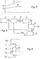
- Figure 1 shows the equivalent diagram of a stepping motor.
- the coil of this motor is represented by a coil 1, of inductivity L and zero resistance, and by a resistance 2, of value R equal to the resistance of the motor coil.
- the voltage source induced in the coil by the rotation of the rotor is symbolized by a voltage source 3.
- the value of this induced voltage is designated by U.
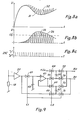
- the curves 4 and 5 of FIG. 2a which are well known, illustrate the variation of the current i in the motor coil as a function of time, during the driving pulse, in cases where the load driven by the motor is low, respectively strong.
- the curves 6 and 7 of FIG. 2b illustrate, in the same load cases, the variation of the voltage U, measured by a device which will be described later.
- Curves 4 and 5 show that, just after the instant t 0 of activation of the driving pulse, the current in the coil increases according to an exponential law, with a time constant equal to L / R, independently of the load. that the motor should drive. The rotor is still stationary and the voltage U is zero r ( Figure 2b).
- the rotor begins to rotate.
- the source 3 begins to supply the voltage U induced by the rotation of the rotor, and the current i in the coil therefore ceases to have an exponential variation. It follows a curve which depends on the load driven by the motor, and of which curves 4 and 5 are two examples.
- the voltage U follows a curve which also depends on the load driven by the motor. Curve 6 in Figure 2b corresponds to curve 4 in Figure 2a, and curve 7 in curve 5.
- the voltage U r goes through a maximum, before going through zero the moment the rotor passes through its equilibrium position with current, that is to say the position which it ends up taking, after a few oscillations, if the driving pulse is not interrupted.
- the voltage U then oscillates around zero until the rotor comes to a stop.
- FIG. 3 illustrates the variation of the minimum duration Tl of the driving pulse necessary to turn an engine as a function of the torque C that this engine must provide.
- This variation is substantially linear and has a fairly low dispersion for a given type of engine. It can be expressed by the relation where T01 is the minimum duration of the driving pulse for a zero load and has the slope of the line.
- T2 put by the voltage U r to reach a determined threshold U has also been reported in this figure 3. It is also substantially linear and can be expressed by the relation where T02 is the time taken by the voltage U r to reach the threshold voltage U in the absence of load and b is the slope of the line.
- k and K can be easily calculated from the measurement of times T01 and T02 and times T1 and T2 for a known load. Once they have been determined, for a type of engine, they can be used in the control circuit of this type of engine, the diagram of which gives the diagram. Figure 5 shows the variation of the signals at some points in this figure 4.
- the reference 8 designates a circuit whose output delivers a signal S8 to a control circuit 9 each time that the motor 10 must advance by one step.
- Circuit 8 can be constituted, by way of nonlimiting example, by the oscillator and the frequency division chain of an electronic watch, and it can be arranged so as to deliver periodic signals having various frequencies. These signals will be described later.
- the control circuit 9 delivers a driving pulse I to the motor 10.
- this motor 10 is a stepping motor as it is commonly used in watches, the correct polarity of the driving pulse 1 is also determined by the circuit 9.
- a measurement circuit 11 is connected to the motor 10. It is arranged, in a manner which examples will be given later, to deliver a voltage U m proportional to the voltage U induced in the motor coil by the rotation of the rotor.
- the measured voltage U m is applied to a detector circuit 12 which delivers a signal S12 at the instant when this voltage U m exceeds a judiciously chosen reference voltage U '.
- a calculation circuit 13 of which exemplary embodiments will be described later, delivers a signal S13 a certain time after having received the signal S12. The instant when this signal S13 is delivered depends on the time which has elapsed between the start of the driving pulse and the appearance of the signal S12, and on the two constants k and K which are also provided, in an adequate form, to the calculation circuit 13.
- the signal S13 is used by the control circuit 9 to interrupt the driving pulse I.
- FIG. 6 gives the block diagram of an example of a circuit 11 for measuring the voltage U.
- This circuit 11 like the other circuits which will be described later, is supplied by a voltage source, not shown.
- This source delivers a positive voltage + U a and a negative voltage -U a with respect to a midpoint which is grounded to the circuit.
- the voltage -U a is intended, in particular, to supply the differential amplifiers used in these circuits.
- FIG. 6 shows the motor 10 connected, in a conventional manner, in a bridge of four MOS transistors 14, 15, 16 and 17 forming part of the control circuit 9 of FIG. 4.
- the transistors 14 and 15, of type p have their sources connected to the positive pole tU a of the power source, not shown.
- Transistors 16 and 17, of type n have their source connected to the ground of the circuit, through a measurement resistor 18, of low value, forming part of the measurement circuit 11 of FIG. 4.
- the drains of transistors 14 and 16 are connected to one of the terminals of the motor 10, and the drains of the transistors 15 and 17 to the other.
- the control electrodes of the four transistors 14 to 17 are connected to a logic circuit, not shown in this figure 6, which delivers the logic signals necessary for the control of these transistors.
- a logic circuit not shown in this figure 6, which delivers the logic signals necessary for the control of these transistors.
- An example of this logic circuit will be given later.
- the measurement circuit 11 includes an amplifier 20 whose input is connected to point 19 common to the sources of the transistors 16 and 17 and to the resistor 18.
- the gain of this amplifier 20 is chosen so that its output voltage U20 is equal at the supply voltage + U a when the current i flowing in the motor coil is equal to U a / R.
- the output of this amplifier 20 is connected to the input of a transmission gate 21, and to the inverting input of a differential amplifier 22.
- the transmission gate 21 is controlled by a logic signal 21C which is supplied, by example, by circuit 8 in FIG. 4, which will be described later.
- This transmission gate 21 is connected to the junction point 23 of a resistor 24, having a value R24, and of a capacitor 25 having a capacitance C25. Point 23 is also connected, through an amplifier 26, to the non-inverting input of the differential amplifier 22.
- the sole purpose of the amplifier 26 is to reduce the load that the input of the amplifier 22 would constitute for the R-C circuit 24-25.
- the gain of this amplifier 26 is chosen to be equal to 1.
- the circuit formed by the resistor 24 and the capacitor 25 is connected between the + U terminal of the power source and the ground.
- the value R24 of resistance 24 and the capacity C25 of capacitor 25 are chosen so that where L and R are, as above, the inductance and resistance of the motor coil.
- the transmission gate 21 When the signal 21C is in the "0" state, the transmission gate 21 is in its blocking state.
- the voltage at point 23 is equal to the output voltage of the amplifier 20.
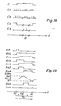
- Figure 7 illustrates the operating principle of this circuit.
- the curve 27 represents the variation, during a driving pulse, of the output voltage U20 of the amplifier 20.
- This curve 27 is an image of the current i which flows in the coil of the motor 10.
- the voltage U23 at point 23 follows the same curve 27.
- the voltage U22 at the output of the differential amplifier 22 therefore remains zero. If, at any time t x , the gate 21 becomes blocking, the voltage U20 continues to follow the curve 27.
- This curve 28 is exactly the same as that which the voltage U20 would follow if, at time t x , the rotor was suddenly blocked, which would cancel the voltage U. It is therefore the image of the current i 'which would flow, under these conditions, in the motor coil.
- the voltage U20 is proportional to the current i which flows in the coil during a driving pulse.
- this current i can be expressed by the relation which is easily deduced from the circuit of FIG. 1 in the case where the voltage + U a is applied to the motor by its control circuit, not shown in this FIG. 1.
- U rx is equal to the length of the segment Z '- Y' in Figure 7, where Y 'and Z' are the points of the tangents 29 and 30 located on the abscissa (t x + ⁇ ).
- the ordinate of point Z ' is equal to U a / R which is the asymptotic value of the exponential 28.
- Figures 8a and 8b illustrate the operation of the circuit of Figure 6 when the transmission gate 21 is controlled by a signal 21C such as that shown in Figure 8c.
- the transmission gate 21 is conductive when the signal 21C is in the logic state "1", and blocked when this signal 21C is in logic state "0".
- the control signal 21C is constituted, for example, by pulses having a period of approximately 250 micro-seconds which are in the logic state "1" for a few microseconds, and in state "0" the rest of the time.
- the transmission gate 21 therefore becomes conductive for a few microseconds every 250 microseconds, and it is blocking the rest of the time.
- the curve 31 again represents the voltage U20, which is an image of the current i in the coil.
- the sawtooth curve 32 which is superposed on it represents the voltage U23. Indeed, each time the transmission gate 21 becomes conductive, that is to say when the signal 21C is in the state "1", the voltage U23 becomes equal to the voltage U20.
- the transmission door 21 is blocking, that is to say when the signal 21C is in the "0" state, the voltage U23 varies according to a curve such as the exponential curve 28 shown in FIG. 7.
- the sawtooth curve 33 of FIG. 8b represents, on a different scale from that of FIG. 8a, the output voltage U22 of the differential amplifier 22.
- This voltage U22 is equal to zero each time the transmission gate 21 is conductive, and it is equal to the difference of the voltages U23 and U20 when the transmission door 21 is blocked.
- the curve 34 which is the envelope of the curve 33, is an image of the voltage U induced in the motor coil by the rotation of the rotor.
- This envelope 34 could be obtained by filtering the voltage U22 in a low-pass filter.
- the output signal of this filter could be amplified in an amplifier, the gain of which would be chosen taking into account all the proportionality factors introduced into the circuit of FIG. 6 by the choice of the measurement resistance 18, of the gain of the amplifier 20 and the period of the control signal 21C.
- the output signal from this amplifier would then be equal to the induced voltage U. But this filtering and this amplification are not necessary.
- the voltage U22 itself can be directly used as the measurement voltage U in the circuit of FIG. 4.
- the voltage U 'at which the voltage U m is compared in circuit 12 of FIG. 4 must of course be chosen taking into account the proportionality factors above.
- the voltage U22 is independent of the supply voltage U, since the voltages U23 and U20 are both proportional to this voltage U.
- Figure 9 shows the block diagram of a measurement circuit 11 ( Figure 4) providing a voltage U ml proportional to U rx based on equation (9) above.
- the resistor 18 for measuring the current flowing in the motor (not shown in this FIG. 9) and the amplifier 20 whose output voltage is an image of this current are identical to the resistor 18 and to the amplifier 20 of FIG. 6.
- the output of amplifier 20 is connected, via diary of a transmission gate 61 to a first terminal of a capacitor 62 of capacitance C62, and to the non-inverting input of a differential amplifier 63.
- the second terminal of the capacitor 62 is connected to the ground of the circuit.
- the output of amplifier 63 is connected to its inverting input.
- the gain of this amplifier is therefore equal to one. Its output is also connected, through two transmission doors 64 and 65, to the first terminals of two capacitors 66 and 67, of capacity C66 and C67.
- the second terminal of the capacitor 66 is connected through a transmission gate 68 to the + U terminal of the power source and the second terminal of the capacitor 67 is connected to the output of the amplifier 20 by a transmission gate 69.
- the first terminal of the capacitor 66 and the second terminal of the capacitor 67 are connected to a first output terminal of the circuit, designated by B1, by transmission gates 70, respectively 71.
- the second terminal of the capacitor 66 and the first terminal of the capacitor 67 are connected to a second output terminal of the circuit, designated by B2, by transmission doors 72, 73 respectively.
- the transmission doors 61 and 70 to 73 are controlled together by a signal designated by C1, and the transmission doors 64, 65, 68 and 69 are controlled, also together, by a signal designated by C2.
- These signals C1 and C2 which can be delivered, for example, by the circuit 8 of FIG. 4, and which are represented in FIG. 10, have identical periods of 0.5 milliseconds for example and equally short durations, compared to their period, 30 microseconds for example. Each of them appears in the middle of the other's period.
- FIG. 7 can also be used to understand the operation of the circuit of FIG. 9.
- the signal C2 makes the transmission doors 64, 65, 68 and 69 conductive.
- the voltage U x memorized by the capacitor 62 and the amplifier 63 is therefore applied to the first terminal of the capacitor 66 and of the capacitor 67.
- the voltage U a is applied to the second terminal of the capacitor 66 and a proportional voltage to the current flowing at this instant t y in the motor coil is applied to the second terminal of the capacitor 67.
- this voltage can be considered to be the voltage U y of FIG. 7.
- the following pulse C1 makes the transmission doors 70 to 73 conductive.
- the capacitors 66 and 67 are therefore connected in parallel with the output terminals B1 and B2 of the circuit.
- the voltage U ml which then appears at these terminals is equal to:
- equation (10) can be written:
- either of the output terminals B1 and B2 can be grounded to the circuit without the operation of the latter being modified.
- the accuracy of the measured value depends directly on the accuracy of the value of the resistor 24 and of the capacitor 25. It is well known that it is difficult, in mass production, to obtain great precision for such elements.
- the circuit of FIG. 9 does not have this drawback.
- the precision of the measurement depends in fact only on the ratio of the capacities of the capacitors 66 and 67. However, even in mass production, this ratio can be guaranteed with very good precision.
- Figure 11 shows the diagram of a third measurement circuit which eliminates this source of error.
- the output terminal BI of the circuit of FIG. 9 is connected to the inverting input of a differential amplifier 74.
- the non-inverting input of this amplifier 74 is connected to ground.
- the output of this amplifier 74 is connected to its inverting input by a capacitor 75 connected in parallel with a transmission gate 76.
- the output of the amplifier 74 is further connected, through a transmission gate 77, to the input non-inverting of a differential amplifier 78.
- a capacitor 79 and a transmission gate 80 are connected in parallel between this non-inverting input of amplifier 78 and ground.
- the output of amplifier 78 constitutes the output of measurement circuit 11. This output is connected to the inverting input of amplifier 78 by a resistor 81 and to the ground of the circuit by a resistor 82.
- the non-input amplifier 78 is further connected by a transmission gate 83 to the non-inverting input of a differential amplifier 84.
- a capacitor 85 and a transmission gate 86 are connected in parallel between this input of the amplifier 84 and the mass.
- the output of amplifier 84 is connected to its inverting input.
- the gain of this amplifier 84 is therefore equal to one. Its output is also connected, by a transmission gate 87, to a first terminal of a capacitor 88. The other terminal of this capacitor 88 is connected to ground. Finally, the first terminal of the capacitor 88 is connected by a transmission gate 89 to the inverting input of the amplifier 74.
- the transmission doors 77 and 89 are controlled by the signal C1 described above, at the same time as the transmission doors 61, 70, 71 and 73.
- the transmission doors 76 and 87 are controlled by the signal C2 also described here above, like the transmission doors 64, 65 and 69.
- the transmission doors 80 and 86 are controlled by a signal C3 which can be, for example, delivered by the circuit 9 for controlling the motor 10 and which is at state "0" during motor pulses and state "1" the rest of the time.
- the doors 80 and 86 are therefore conductive between the driving pulses and blocked during these driving pulses.
- the transmission gate 83 is controlled by a signal C4 which is normally at "0" and which passes to the state "1" for a few microseconds approximately one millisecond after the start of the driving pulse.
- Signals C3 and C4 are also shown in Figure 10.
- Equation (11) above in which the term U a is replaced by 0 shows that the voltage U m2 which would appear at terminal B1 in response to the signal C1 if the elements 74 to 89 did not exist would be:
- the capacitor 88 is discharged since the output of the amplifier 84, which is grounded, is connected to it at each pulse C2 by the transmission gate 87.
- the capacitor 75 is also discharged through the transmission door 76 which short-circuits it. Immediately after each of these pulses C2, the output of the amplifier 74 is therefore also at ground potential.
- a pulse C1 makes the transmission gates 70, 71, 73, 77 and 89 conductive.
- the sum of the charges contained at this time in the capacitors 66, 67 and 88 is therefore transferred to the capacitor 75.
- the voltage U75 at the terminals of this capacitor would then be: if the transmission door 80 was not conductive.
- the sign - which appears in this equation results from the fact that terminal B1 is connected to the inverting input of amplifier 74.
- this voltage U75 remains zero as long as the signal C3 is in the state "1" and the charges Q66 and Q67 are transmitted to ground by this transmission gate 80.
- the charge Q88 of the capacitor 88 is in any case zero at this moment.
- the output of amplifier 78 therefore remains at ground potential.
- the C4 pulse is produced approximately one millisecond after the start of the driving pulse, at a time when the rotor is still stationary.
- This pulse C4 briefly opens the transmission gate 83.
- the capacitor 85 is therefore charged at this voltage U75 D which also appears at the output of the amplifier 84.
- the pulse C2 following this pulse C4 opens the transmission gate 87 and the capacitor 88 therefore also charges at voltage U75 D.
- the electrical charge Q88 of the capacitor 88 therefore becomes equal to:
- the capacitor 85 remains practically charged at the voltage U75 D as long as the transmission gate 86 remains blocked, if the input resistance of the amplifier 84 is large, which is the case. Subsequent changes in the output voltage of amplifier 74 no longer have any influence on this voltage since the transmission gate 83 is permanently blocked again.
- the capacitor 88 discharges into the capacitor 75, at the same time as the capacitors 66 and 67.
- the charge of the capacitor 75 therefore becomes
- the capacitor 88 recharges at the voltage U75 D which is memorized by the capacitor 85.
- This voltage U75 is independent of the voltage U, or of the voltage U a '. In addition, it is proportional to the voltage U rx induced in the motor coil at time t x by the rotation of the rotor. Indeed, at time D defined above, the voltage U m2 given by equation (12) is written:
- Equation (14) above can therefore be written: as a function of the characteristics of the various components of the circuit of FIG. 11, in particular of the capacities of the various capacitors and of the gains of the amplifiers.
- FIG. 12 shows an example of a circuit realizing the function of the circuits 9, 12 and 13 of FIG. 4.
- the circuit 12 is constituted by a simple differential amplifier 41.
- the voltage U constituted by the output voltage of one of the circuits 11 described above, is applied to the non-inverting input of this amplifier 41, the inverting input of which receives a voltage U s ′ chosen as explained above.
- This voltage U ′ can be supplied by a separate source or by a simple voltage divider connected to the terminals of the source supplying the entire circuit.
- the control circuit 9 of the motor 10 comprises the transistors 14 to 17 described in connection with FIG. 6. It also comprises a type D flip-flop 42 whose clock input Ck is connected to the output S8 of circuit 8 of FIG. 4. The input D of this flip-flop 42 is connected to its inverse output Q * so that it changes state each time the signal S8 passes from the logic state "0" in logic state "1".
- the direct output Q of the flip-flop 42 is connected to a first input of an AND gate 43 whose output is connected to the control electrodes of the transistors 14 and 16.
- the output Q * of the flip-flop 42 is connected to a first input of an AND gate 44, the output of which is connected to the control electrodes of the transistors 15 and 17.
- the control circuit 9 also comprises a flip-flop 45, of type D, the clock input Ck of which is connected to the output S8 of the circuit 8 by means of an inverter 58.
- This flip-flop 45 is permanently in the logic state "1", and its output Q is connected to the second input of the gates 43 and 44.
- the calculation circuit 13 comprises a flip-flop 46, also of type D, whose clock input Ck is connected to the output S8 of circuit 8 and whose input D is permanently in the logic state "1 ".
- the outputs Q and Q * of the flip-flop 46 are respectively connected to the first inputs of two AND gates 47 and 48, the second inputs of which are connected, together, to the output Q of the flip-flop 45.
- the voltage U m1 is proportional to the voltage U
- the voltage U75 is also proportional.
- the reset input R of the flip-flop 46 is connected to the output of the differential amplifier 41.
- Three transmission doors 49, 50 and 51 have their control input respectively connected to the outputs of doors 47 and 48, and to the output Q * of the flip-flop 45. These transmission doors 49, 50 and 51 are similar to the door transmission 21 of FIG. 6. When their command input is in logic state "0", they are in their blocking state and when their command input is in logic state "1", they are in their state driver.
- the transmission door 49 is connected between the positive pole + Uade the power source and a resistor 52, of value R52.
- the transmission door 50 is connected between the negative pole -U of the power source and a resistor 53, of value R53.
- the transmission door 51 is connected between a voltage U be which will be defined below, and a resistor 54, of value R54.
- the second terminals of resistors 52, 53 and 54 are connected to each other and to the inverting input of a differential amplifier 55, the non-inverting input of which is connected to a determined voltage, which is that of ground in the present example. .
- a capacitor 56 of capacity C56, is connected between the common point of the resistors 52 to 54 and the ground.
- the output of the amplifier 55 is connected to a first input of an AND gate 57 whose second input is connected to the output Q * of the flip-flop 46.
- the output of this gate 57 is connected to the input R of resetting the flip-flop 45.
- the voltage U56 across the capacitor 56 is therefore equal to the voltage U b . If this voltage is positive, as in this example, the outputs of amplifier 55 and of gate 57 are at "0".
- the output of gate 57 therefore changes to "0", even if the output of amplifier 55 is at "1" at this time.
- the output of gate 43 therefore also changes to "1".
- the transistor 14 is blocked and the transistor 16 becomes conductive.
- the current i begins to circulate in the coil of the motor 10, through the transistors 15 and 16.
- the voltage at point 19 begins to increase and act on the measurement circuit 11 as has been explained with reference to FIGS. 6, 9 or 12.
- the output Q * of the flip-flop 45 changes to "0", which blocks the transmission door 51.
- the output of the door 47 changes to "1", which makes the transmission door 49 conductive.
- the voltage + U a is therefore applied to the capacitor 56 through the resistor 52, and the voltage U56 begins to increase according to an exponential curve having a time constant il determined by the product R52.C56.
- the variation of the voltage U56 has been represented, in FIG. 13, as a linear variation.
- the output of the amplifier 41 changes to "1".
- the output Q of the flip-flop 46 therefore returns to "0", which causes the blocking of the transmission door 49.
- the value U d reached by the voltage U56 at time t d depends on the time T2 taken by the induced voltage U to reach the threshold voltage U, the value of the voltage U b and the time constant ⁇ 1.
- this flip-flop 46 goes to "1", which makes the transmission gate 50 conductive.
- the voltage -U a is therefore now applied to the capacitor 56 through the resistor 53.
- the voltage U56 therefore begins to decrease, from the value U d , with a time constant 12 determined by the product R53.C56.
- this voltage U56 becomes equal to a determined voltage, which is the voltage of the ground in the present example
- the output of the amplifier 55 changes to "1”, which resets the flip-flop 45 in its rest state, that is to say with its Q output at "0" and its Q * output at "1".
- the output of the gate 43 therefore returns to "0", which blocks the transistor 16 and makes the transistor 14 conductive.
- the current i is therefore interrupted, and the rotor of the motor ends its pitch thanks to its inertia and thanks to a part energy that is stored, in the form of magnetic energy, in the inductance of the coil.
- the rotor is braked by the short circuit which is established through the transistors 14 and 15.
- the time T3 taken by the voltage U56 to become equal to zero depends on the voltage U d that it had reached at the instant t d and on the time constant ⁇ 2.
- the duration Tl of the driving pulse is equal to the sum of the durations T2 and T3. As T3 depends on the voltage U of and this voltage U d itself depends on the duration T2, we see that this duration Tl depends directly on the time T2 put by the voltage U induced in the motor coil by the rotation of the rotor to reach a predetermined U value.
- the duration TOI of the driving impulse necessary to run the motor without load the time T02 put by the induced voltage U r to reach the value U s when the motor is also without load, and the coefficients a and b of the lines which represent the variation as a function of the motor load of the duration of the driving pulse and of the time taken by the voltage U r to reach the threshold U s , it is easy to determine the time constant t1 and t2 as well as the voltage U b so that the relation (1) mentioned above is verified. It is therefore in the form of these parameters ⁇ 1, t2 and U b that the constants k and K of this relation (1) are introduced in the present example of the calculation circuit 13.
- the voltage U b can be chosen negative, if necessary, to take account of the sign of the constant K.
- the state "0" of the output Q of the flip-flop 45 causes the blocking of the transmission gate 50.
- the state “1" of the output Q * of this flip-flop 45 makes the conductive transmission door 51.
- the voltage U b is therefore again applied to the capacitor 56 through the resistor 54.
- the voltage U56 therefore increases again, until it reaches, after a certain time, the voltage U b .
- FIG. 14 illustrates another example of a circuit realizing the function of the calculation circuit 13 of FIG. 4.
- This circuit comprises a flip-flop 91, of type D, the clock input Ck of which receives the signal S8 from the output of circuit 8 in FIG. 4.
- the input D of this flip-flop 91 is permanently at l 'logical state "1".
- Its output Q is connected to the U / D input for determining the counting direction of a reversible counter 92.
- This counter 92 is also preselectable, which means that, in response to a pulse on a control input C, its content takes a value determined by the logic states "0" or "1" which are applied to preselection inputs designated together by P.
- control input C of the counter 92 is also connected to the output S8 of the circuit 8, and its inputs P are connected, in a fixed or modifiable manner which will be described below, to the potentials representing the logic states "0" and "1".
- the counter 92 also includes a clock input Ck which is connected to the output of an OR gate 93 whose inputs are respectively connected to the outputs of two AND gates 94 and 95.
- gate 94 The inputs of gate 94 are respectively connected to the output Q of the flip-flop 45 of FIG. 12, not shown in this FIG. 14, to the output Q of the flip-flop 91, and to a circuit, also not shown, which delivers a periodic signal having a frequency fl.
- This circuit can be circuit 8 in FIG. 4 and the frequency f1 is chosen in a manner which will be described later.
- gate 95 The inputs of gate 95 are respectively connected to the output Q of the flip-flop 45, to the output Q * of the flip-flop 91 and to a circuit, which can also be circuit 8 of FIG. 4, and which delivers a periodic signal having a frequency f2, the choice of which will also be described below.
- the outputs of counter 92 are connected to a detection circuit 96, the output of which takes the state "1" when the content of counter 92 is equal to zero.
- This detection circuit 96 can simply consist of a reverse OR gate, each input of which is connected to an output of the counter 92.
- This detection circuit 96 is connected to an input of an AND gate 97, the other input of which is connected to the output of the flip-flop 91.
- gate 97 is connected to the reset input R of flip-flop 45 of FIG. 12, not shown in FIG. 14.
- the value Nd of the content of the counter 92 at this instant depends on the time T2 'taken by the induced voltage U to reach the threshold voltage U, of the initial value Ni taken by the content of this counter 92 in response to the signal S8, and of the frequency fl.
- the time T3 'taken by the counter 92 to reach the zero state depends on the value Nd reached by its content at the time when the output S12 of the circuit 12 changes to the state "1" and on the frequency f2.
- the duration Tl 'of the driving pulse is equal to the sum of the durations T2' and T3 '.
- the duration T3 ' depends on the value Nd, and since this value Nd itself depends on the duration T2', the duration Tl 'of the driving pulse depends directly on the time T2' put by the voltage U induced in the coil of the motor by the rotation of the rotor to reach the predetermined value U.
- the frequencies fl and f2 play the role of the cons time uncles ⁇ 1 and ⁇ 2 in the case of FIG. 12, and the initial value Ni plays that of the voltage Ub.
- a negative initial value Ni must be introduced into the counter 92.
- the value of the content of a counter is always a positive number, in this case it is necessary to enter into the counter 92 an initial value Ni 'equal to the difference between the counting capacity of the counter 92 and the absolute value of Ni.
- the content of the counter 92 goes through zero after Ni frequency pulses f1 have been received by its input Ck. But as at this moment the output Q * of the flip-flop 91 is still in the state "O", the signal "1" delivered by the output of the circuit 96 is blocked by the gate 97. The driving pulse is not therefore not interrupted at this time.
Landscapes
- Physics & Mathematics (AREA)
- General Physics & Mathematics (AREA)
- Control Of Stepping Motors (AREA)
- Tests Of Circuit Breakers, Generators, And Electric Motors (AREA)
- Measurement Of Current Or Voltage (AREA)
- Electromechanical Clocks (AREA)
- Electrical Discharge Machining, Electrochemical Machining, And Combined Machining (AREA)
Applications Claiming Priority (2)
| Application Number | Priority Date | Filing Date | Title |
|---|---|---|---|
| CH182681A CH644989GA3 (de) | 1981-03-18 | 1981-03-18 | |
| CH1826/81 | 1981-03-18 |
Related Parent Applications (1)
| Application Number | Title | Priority Date | Filing Date |
|---|---|---|---|
| EP82810024.8 Division | 1982-01-21 |
Publications (3)
| Publication Number | Publication Date |
|---|---|
| EP0137093A2 true EP0137093A2 (de) | 1985-04-17 |
| EP0137093A3 EP0137093A3 (en) | 1985-05-29 |
| EP0137093B1 EP0137093B1 (de) | 1988-06-01 |
Family
ID=4219497
Family Applications (2)
| Application Number | Title | Priority Date | Filing Date |
|---|---|---|---|
| EP82810024A Expired EP0060806B1 (de) | 1981-03-18 | 1982-01-21 | Verfahren zur Reduzierung der Leistungsaufnahme eines Schrittmotors und Vorrichtung zur Durchführung dieses Verfahrens |
| EP84101561A Expired EP0137093B1 (de) | 1981-03-18 | 1982-01-21 | Verfahren zur Messung der in die Wicklung eines Schrittmotors durch Drehung seines Rotors induzierten Spannung |
Family Applications Before (1)
| Application Number | Title | Priority Date | Filing Date |
|---|---|---|---|
| EP82810024A Expired EP0060806B1 (de) | 1981-03-18 | 1982-01-21 | Verfahren zur Reduzierung der Leistungsaufnahme eines Schrittmotors und Vorrichtung zur Durchführung dieses Verfahrens |
Country Status (5)
| Country | Link |
|---|---|
| US (2) | US4446413A (de) |
| EP (2) | EP0060806B1 (de) |
| JP (2) | JPS57153599A (de) |
| CH (1) | CH644989GA3 (de) |
| DE (1) | DE3276268D1 (de) |
Cited By (2)
| Publication number | Priority date | Publication date | Assignee | Title |
|---|---|---|---|---|
| EP0305876A3 (de) * | 1987-08-31 | 1990-06-13 | AlliedSignal Inc. | Wellenstellungsfühler eines Schrittmotors |
| FR2668866A1 (fr) * | 1990-11-07 | 1992-05-07 | Ebauchesfabrik Eta Ag | Procede de commande d'un moteur pas a pas et dispositif pour la mise en óoeuvre de ce procede. |
Families Citing this family (10)
| Publication number | Priority date | Publication date | Assignee | Title |
|---|---|---|---|---|
| CH646575GA3 (de) * | 1981-10-02 | 1984-12-14 | ||
| US4556836A (en) * | 1983-05-24 | 1985-12-03 | Societe Industrielle De Sonceboz S.A. | Multiphase motor damping method and circuit arrangement |
| CH653850GA3 (de) * | 1983-08-12 | 1986-01-31 | ||
| CH653206GA3 (de) * | 1983-09-16 | 1985-12-31 | ||
| CH663701A5 (de) * | 1984-04-10 | 1987-12-31 | Sodeco Compteurs De Geneve | Verfahren und einrichtung zur steuerung eines von einer gleichspannung gespeisten schrittmotors. |
| JPS6225894A (ja) * | 1985-07-25 | 1987-02-03 | Silver Seiko Ltd | ステツピングモ−タの駆動装置 |
| JPS6292799A (ja) * | 1985-10-17 | 1987-04-28 | Silver Seiko Ltd | ステツピングモ−タの駆動装置 |
| EP0253153B1 (de) * | 1986-07-02 | 1991-08-28 | Asulab S.A. | Verfahren und Vorrichtung zur Kontrolle eines Schrittmotors |
| DE4339553C1 (de) * | 1993-11-19 | 1995-06-22 | Sgs Thomson Microelectronics | Treiberschaltung für einen Schrittmotor |
| EP3663870B1 (de) * | 2018-12-06 | 2021-08-11 | The Swatch Group Research and Development Ltd | Elektromotor mit asymmetrischen statorinduktoren |
Family Cites Families (11)
| Publication number | Priority date | Publication date | Assignee | Title |
|---|---|---|---|---|
| CH1372372A4 (de) * | 1972-09-20 | 1976-09-15 | ||
| JPS6024680B2 (ja) * | 1973-03-07 | 1985-06-14 | セイコーインスツルメンツ株式会社 | 時計用ステツプモ−タの駆動回路 |
| JPS5292560A (en) * | 1976-01-29 | 1977-08-04 | Seiko Instr & Electronics Ltd | Switch box drive pulse width control circuit for electronic clocks |
| US4158287A (en) * | 1976-08-12 | 1979-06-19 | Citizen Watch Company Limited | Driver circuit for electro-mechanical transducer |
| JPS5370874A (en) * | 1976-12-07 | 1978-06-23 | Seiko Epson Corp | Electronic wristwatch |
| CH635973B (fr) * | 1977-01-19 | Suwa Seikosha Kk | Circuit de commande pour un transducteur electromecanique d'une montre, notamment d'une montre-bracelet electronique. | |
| JPS5412777A (en) * | 1977-06-29 | 1979-01-30 | Citizen Watch Co Ltd | Pulse motor driving circuit for watches |
| CH616819GA3 (en) * | 1977-08-05 | 1980-04-30 | Electronic watch including a corrector circuit | |
| JPS5619473A (en) * | 1979-07-27 | 1981-02-24 | Citizen Watch Co Ltd | Electronic timepiece |
| DE2944872C2 (de) * | 1979-11-07 | 1981-11-19 | Gebrüder Junghans GmbH, 7230 Schramberg | Anordnung zur Steuerung eines Schrittmotors für batteriebetriebene Geräte |
| CH640999B (fr) * | 1980-08-25 | Ebauchesfabrik Eta Ag | Procede et dispositif de commande d'une moteur pas a pas de piece d'horlogerie electronique. |
-
1981
- 1981-03-18 CH CH182681A patent/CH644989GA3/fr unknown
-
1982
- 1982-01-21 EP EP82810024A patent/EP0060806B1/de not_active Expired
- 1982-01-21 DE DE8282810024T patent/DE3276268D1/de not_active Expired
- 1982-01-21 EP EP84101561A patent/EP0137093B1/de not_active Expired
- 1982-02-03 JP JP57014998A patent/JPS57153599A/ja active Granted
- 1982-02-04 US US06/345,952 patent/US4446413A/en not_active Expired - Lifetime
-
1984
- 1984-02-15 US US06/580,305 patent/US4568867A/en not_active Expired - Fee Related
- 1984-02-24 JP JP59032728A patent/JPS6096198A/ja active Pending
Cited By (4)
| Publication number | Priority date | Publication date | Assignee | Title |
|---|---|---|---|---|
| EP0305876A3 (de) * | 1987-08-31 | 1990-06-13 | AlliedSignal Inc. | Wellenstellungsfühler eines Schrittmotors |
| FR2668866A1 (fr) * | 1990-11-07 | 1992-05-07 | Ebauchesfabrik Eta Ag | Procede de commande d'un moteur pas a pas et dispositif pour la mise en óoeuvre de ce procede. |
| EP0484770A1 (de) * | 1990-11-07 | 1992-05-13 | Eta SA Fabriques d'Ebauches | Verfahren zur Steuerung eines Schrittmotors und Vorrichtung zur Durchführung dieses Verfahrens |
| US5280226A (en) * | 1990-11-07 | 1994-01-18 | Eta Sa Fabriques D'ebauches | Method and device for controlling a stepping motor by interrupting its drive pulse |
Also Published As
| Publication number | Publication date |
|---|---|
| CH644989GA3 (de) | 1984-09-14 |
| US4446413A (en) | 1984-05-01 |
| US4568867A (en) | 1986-02-04 |
| EP0060806A1 (de) | 1982-09-22 |
| EP0137093B1 (de) | 1988-06-01 |
| JPS57153599A (en) | 1982-09-22 |
| EP0137093A3 (en) | 1985-05-29 |
| JPS6363000B2 (de) | 1988-12-06 |
| DE3276268D1 (en) | 1987-06-11 |
| EP0060806B1 (de) | 1987-05-06 |
| JPS6096198A (ja) | 1985-05-29 |
Similar Documents
| Publication | Publication Date | Title |
|---|---|---|
| EP0171635B1 (de) | Vorrichtung und Verfahren zur Erkennung der Rotorposition eines Schrittmotors | |
| EP0083303B1 (de) | Quarzzeitbezugssignalgenerator mit Temperaturkompensation und Uhr mit diesem Signalgenerator | |
| EP0679968A1 (de) | Uhr mit mechanischem Antrieb und mit elektronischer Steuerung | |
| EP0762243B1 (de) | Uhr mit Gangreserveanzeige | |
| EP0060806B1 (de) | Verfahren zur Reduzierung der Leistungsaufnahme eines Schrittmotors und Vorrichtung zur Durchführung dieses Verfahrens | |
| EP0253227B1 (de) | Vorrichtung zum Programmieren einer nichtflüchtigen Speichervorrichtung für ein Uhrwerk | |
| EP3037898B1 (de) | Elektromechanisches gerät, das einen kapazitiven detektor der winkelposition eines mobilen elementes umfasst, und verfahren zur detektion der winkelposition eines mobilen elementes | |
| FR2752070A1 (fr) | Piece d'horlogerie electronique comportant une generatrice entrainee par un barillet a ressort | |
| CH684862B5 (fr) | Pièce d'horlogerie analogique comportant des moyens d'avertissement d'un changement de mode. | |
| EP0806710A1 (de) | Stabilisation einer elektronischen Schaltung zur Regelung des mechanischen Gangwerks einer Zeitmessvorrichtung | |
| EP0077293B1 (de) | Verfahren und Vorrichtung zur Steuerung eines Schrittmotors in einem Uhrwerk | |
| FR2489055A1 (fr) | Procede pour reduire la consommation en energie du moteur pas a pas d'une piece d'horlogerie electronique et piece d'horlogerie electronique mettant en oeuvre ce procede | |
| EP0253153B1 (de) | Verfahren und Vorrichtung zur Kontrolle eines Schrittmotors | |
| EP0135104B1 (de) | Verfahren und Vorrichtung zum Ansteuern eines Schrittmotors | |
| EP3171231A1 (de) | Stossdetektorschaltkreis und sein funktionsverfahren | |
| CH687727B5 (fr) | Instrument horaire notamment une montre-bracelet electrique du type analogique. | |
| EP0087387A1 (de) | Verfahren und Einrichtung zum Steuern eines umsteuerbaren Schrittmotors | |
| EP0024737A1 (de) | Detektor für die Fortbewegung eines Schrittmotors | |
| EP0076780B1 (de) | Verfahren zur Reduzierung des Verbrauchs eines Schrittmotors und Vorrichtung zur Durchführung dieses Verfahrens | |
| EP0203330B1 (de) | Elektronisches Uhrwerk mit Detektion für den Ablauf der Lebensdauer der Batterie | |
| EP0108711B1 (de) | Verfahren und Vorrichtung zur Steuerung eines Schrittmotors | |
| EP0140089B1 (de) | Verfahren zur Steuerung eines Schrittmotors | |
| CH672572B5 (de) | ||
| FR2585901A3 (fr) | Procede et dispositif de commande d'un moteur a deux bobines | |
| EP0250862A1 (de) | Verfahren und Vorrichtung zum Steuern eines Schrittmotors |
Legal Events
| Date | Code | Title | Description |
|---|---|---|---|
| PUAI | Public reference made under article 153(3) epc to a published international application that has entered the european phase |
Free format text: ORIGINAL CODE: 0009012 |
|
| PUAL | Search report despatched |
Free format text: ORIGINAL CODE: 0009013 |
|
| AC | Divisional application: reference to earlier application |
Ref document number: 60806 Country of ref document: EP |
|
| AK | Designated contracting states |
Designated state(s): DE FR GB |
|
| AK | Designated contracting states |
Designated state(s): DE FR GB |
|
| 17P | Request for examination filed |
Effective date: 19850618 |
|
| 17Q | First examination report despatched |
Effective date: 19861103 |
|
| D17Q | First examination report despatched (deleted) | ||
| GRAA | (expected) grant |
Free format text: ORIGINAL CODE: 0009210 |
|
| AC | Divisional application: reference to earlier application |
Ref document number: 60806 Country of ref document: EP |
|
| AK | Designated contracting states |
Kind code of ref document: B1 Designated state(s): DE FR GB |
|
| REF | Corresponds to: |
Ref document number: 3278583 Country of ref document: DE Date of ref document: 19880707 |
|
| GBT | Gb: translation of ep patent filed (gb section 77(6)(a)/1977) | ||
| PLBE | No opposition filed within time limit |
Free format text: ORIGINAL CODE: 0009261 |
|
| STAA | Information on the status of an ep patent application or granted ep patent |
Free format text: STATUS: NO OPPOSITION FILED WITHIN TIME LIMIT |
|
| 26N | No opposition filed | ||
| PGFP | Annual fee paid to national office [announced via postgrant information from national office to epo] |
Ref country code: GB Payment date: 19901218 Year of fee payment: 10 |
|
| PGFP | Annual fee paid to national office [announced via postgrant information from national office to epo] |
Ref country code: FR Payment date: 19910115 Year of fee payment: 10 |
|
| PGFP | Annual fee paid to national office [announced via postgrant information from national office to epo] |
Ref country code: DE Payment date: 19910119 Year of fee payment: 10 |
|
| PG25 | Lapsed in a contracting state [announced via postgrant information from national office to epo] |
Ref country code: GB Effective date: 19920121 |
|
| REG | Reference to a national code |
Ref country code: GB Ref legal event code: PCNP |
|
| PG25 | Lapsed in a contracting state [announced via postgrant information from national office to epo] |
Ref country code: FR Effective date: 19920930 |
|
| PG25 | Lapsed in a contracting state [announced via postgrant information from national office to epo] |
Ref country code: DE Effective date: 19921001 |
|
| REG | Reference to a national code |
Ref country code: FR Ref legal event code: ST |