EP0137149B1 - Méthode et moyens d'accès très rapide à une mémoire - Google Patents
Méthode et moyens d'accès très rapide à une mémoire Download PDFInfo
- Publication number
- EP0137149B1 EP0137149B1 EP84108331A EP84108331A EP0137149B1 EP 0137149 B1 EP0137149 B1 EP 0137149B1 EP 84108331 A EP84108331 A EP 84108331A EP 84108331 A EP84108331 A EP 84108331A EP 0137149 B1 EP0137149 B1 EP 0137149B1
- Authority
- EP
- European Patent Office
- Prior art keywords
- row
- column
- bits
- address
- memory
- Prior art date
- Legal status (The legal status is an assumption and is not a legal conclusion. Google has not performed a legal analysis and makes no representation as to the accuracy of the status listed.)
- Expired
Links
- 238000000034 method Methods 0.000 title claims description 10
- 230000000295 complement effect Effects 0.000 claims description 8
- 230000003213 activating effect Effects 0.000 claims description 4
- 230000004044 response Effects 0.000 claims description 4
- 240000007320 Pinus strobus Species 0.000 description 26
- 230000006870 function Effects 0.000 description 11
- 230000001934 delay Effects 0.000 description 7
- 238000010586 diagram Methods 0.000 description 6
- 238000001514 detection method Methods 0.000 description 3
- 230000001419 dependent effect Effects 0.000 description 2
- 230000000694 effects Effects 0.000 description 2
- 230000008569 process Effects 0.000 description 2
- 230000008901 benefit Effects 0.000 description 1
- 230000008859 change Effects 0.000 description 1
- 239000012141 concentrate Substances 0.000 description 1
- 230000007423 decrease Effects 0.000 description 1
- 230000002708 enhancing effect Effects 0.000 description 1
- 230000004048 modification Effects 0.000 description 1
- 238000012986 modification Methods 0.000 description 1
- 238000012544 monitoring process Methods 0.000 description 1
- 230000009467 reduction Effects 0.000 description 1
- 239000004065 semiconductor Substances 0.000 description 1
- 239000013589 supplement Substances 0.000 description 1
- 230000007704 transition Effects 0.000 description 1
Images



Classifications
-
- G—PHYSICS
- G11—INFORMATION STORAGE
- G11C—STATIC STORES
- G11C7/00—Arrangements for writing information into, or reading information out from, a digital store
- G11C7/22—Read-write [R-W] timing or clocking circuits; Read-write [R-W] control signal generators or management
-
- G—PHYSICS
- G11—INFORMATION STORAGE
- G11C—STATIC STORES
- G11C8/00—Arrangements for selecting an address in a digital store
- G11C8/18—Address timing or clocking circuits; Address control signal generation or management, e.g. for row address strobe [RAS] or column address strobe [CAS] signals
Definitions
- the invention relates to high speed memory accessing means and method.
- RAM dynamic Random Access Memory
- This arrangement requires that half of the necessary address bits be consecutively placed on the address bus (e.g., first the row address bits and then the column address bits). No accurate memory access can, of course, occur until the entire address has been strobed into the memory. Reducing the time required to strobe in the row address bits, switch the bits on the address bus from row address bits to column address bits, and then strobe these column address bits into the memory is, therefore, critical to enhancing the speed of memory operations.
- Previous memory systems rely on fixed delays to properly control memory accesses via a multiplexed address bus.
- a first fixed delay line has been used to ensure that sufficient time has elapsed between generation of the row address strobe (RAS) bits and the switching of the address bus from row address bits to column address bits. During this first fixed delay period the row address bits present on the address bus are strobed into the memory by the RAS bits. If the first fixed delay is set too short, the row address bits will not be strobed into the memory before the row address bits are replaced by column address bits. This would result in the erroneous addressing and subsequent accessing of an unwanted memory location. If this first fixed delay is set too long the memory access times will be unnecessarily long and memory and associated system operations will, therefore, be slower.
- RAS row address strobe
- the second fixed delay line employed in current memory systems is inserted between switching the address bus from row to column address bits and the generation of column address strobe (CAS) bits which strobe these column address bits into the memory.
- This second fixed delay ensures that a sufficient amount of time elapses between these two events so that all the bits on the address bus will indeed be column address bits and not prior row address bits which have yet to be switched or are in the process of being switched to column address bits.
- the wrong memory location will be addressed and then accessed if the second fixed delay is set too short and memory operations will be unduly long if this second fixed delay is set too long.
- the two fixed delays used in previous memory systems are also not located on the same integrated circuit as the RAS generator, CAS generator and the address bus multiplexor (e.g., due to temperature induced circuit timing delays, power supply variations or technology variations). This can result in a lack of tracking between the fixed delay lines and the RAS and CAS generators and the address bus multiplexor. This lack of tracking may require setting the two fixed delay periods longer than actually necessary in order to ensure that these delays will not be seen as too short due to tracking differences. The result is an accurate, but slowly operating memory system.
- a measure of increased accuracy can be obtained by incorporating function completion detectors in the circuitry alongside the function circuits that they monitor, see, for example, US-A-3 962 686, in which there is a detector 11 which detects when the address buffer is loaded and generates a signal 01 which activates the address decoder, in turn, monitored by circuit 31 which causes signal 02 to be issued when the decoding function is complete, and so on.
- a detector 11 which detects when the address buffer is loaded and generates a signal 01 which activates the address decoder, in turn, monitored by circuit 31 which causes signal 02 to be issued when the decoding function is complete, and so on.
- T1 between detection of loading of the address buffer and the generation of 01
- T2 between the functioning of the address decoder and the generation of 02.
- This function monitoring may be efficient in the context of the memory organisation of that patent as no function circuitry is shared, particularly the address bus, as is the case with the kind of memory with which this invention is concerned, illustrated in general terms in, for example "INTEL, THE SEMICONDUCTOR MEMORY BOOK", 1978, pages 156-159, Fielland, published by John Wiley and Sons in New York or in Fig. 1 of this specification.
- the present invention provides a memory, notionally organised into rows and columns and including an apparatus for accessing a selected location within a memory in terms of row and column addresses, the apparatus comprising
- the present invention provides a method internal to a memory for accessing a selected location within the memory when notionally organised by rows and columns, the method comprising the steps of:
- the delay is initiated by activating a dynamic delay element of substantially the same technology as the generating circuitry and packaged therewith, in response to the start of a memory access cycle;
- the row/column address bits are strobed as complementary bit pairs and the column/row address bits are strobed as identical bit pairs;
- the column/row strobe bits are generated in response to and immediately after it has been detected that the last to settle of the plurality of column/row address bit pairs has settled from complementary to identical bit pairing whereby the time required to access a selected location within the memory is reduced as a result of the efficient multiplexing of the plurality of row address bits and plurality of the column address bits.
- a dynamic delay element is activated after all of the bits in the first group of address strobe bits have been generated. After this time delay period has elapsed, a second group of address bits is multiplexed onto the address bus. After this multiplexing is completed a second group of address strobe bits is generated to strobe the second group of address bits into the memory.
- a logic gate is used as a detection means to ascertain when the multiplexing is completed and thus enable the generation of the second group of address strobe bits.
- tracking among inter-related functions is realised by placing these functions on a single integrated circuit.
- Such an arrangement substantially reduces memory access time as a result of the efficient multiplexing of the first and second groups of address bits.
- the dynamic delay element and the logical detection means of the present arrangement replace the two relatively expensive and unreliable fixed delay lines of previous memory systems. Unlike previous memory systems, the present arrangement allows the dynamic delay element to be activated as soon as all RAS bits are generated. The memory access is also not dependent on a fixed, error-prone delay time. Moreover, the present arrangement speeds memory access by generating the strobe address bits associated with the second group of address bits as soon as the multiplexing of bits on the address bus has been completed. Again there is no dependence on a fixed error-prone delay as with current memory systems.
- the memory access speed is optimised by permitting the access to occur as fast as possible by eliminating excess delay times previously inherent in off-chip fixed delay lines through the use of an integrated dynamic timing technique and apparatus.
- the present arrangement should also result in a lower noise level on a memory card because simultaneous driver switching is minimised.
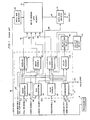
- Fig. 1 illustrates an example of a memory system which includes a memory 10 and an access control circuit 11. Circuit 11 has sometimes been placed on a single integrated circuit.
- Memory 10 typically resides on one card. This card is comprised of several individual integrated circuit dynamic RAM modules.
- One or more processors 9 write data into memory 10 via input data bus 12 and read data out of memory 10 via output data bus 13.
- the data read out of memory 10 via output data bus 13 passes through a plurality of data bus drivers 14 (one driver is provided for each bit in an output data word) to ensure that that data is sufficiently powered to reach its destination.
- Data written into memory 10 passes through a plurality of data bus receivers 19 (one receiver is also typically provided for each bit in the input data word).
- a processor which reads/writes data from/to memory 10 selects the location within memory 10 that the data is to be read from or written into via address bus 15.
- the processor generates row and column address bits and places them on row address bus 16 and column address bus 17, respectively. These row and column address bits are routed to an address multiplexor 18. Multiplexor 18 switches the row address bits and then column address bits (or vice versa) onto address bus 15. This multiplexing of groups of address bits is necessary because the width of address bus 15 is such that only part of the complete address (e.g., half) can be routed to memory 11 at one time.
- the processor In addition to generating the address of a selected location for a particular memory operation, the processor must also generate several other signals. Because several cards like memory 10 may be typically combined to form a large memory (each card accommodating a plurality of RAM modules), it is necessary to supplement the basic row and column address bits (which serve to select a specific location within one or a group of RAM modules) with selection signals which route the row and column address bits to the appropriate RAM module(s). Wire card lines 20 are set up by board wiring to assign a unique address to each card which accommodates a memory 10. Comparator 21 compares the card select signal 22 generated by the processor with the unique address on wire card line 20. If these signals are the same the valid card signal 23 is activated and the designated card selected.
- the Row Address Strobe (RAS) 24, Column Address Strobe (CAS) 25 and Write Enable 26 signals (which are generated by RAS generator 35, CAS generator 36 and write enable 37, respectively) can only be gated to a selected RAM module(s) when the valid card signal 23 is activated.
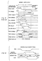
- Fig. 2 illustrates the timing relationships among the various signals involved in a memory read cycle.
- a read operation is initiated by the Array Select line 29 going active while the Write Enable Line 30 is inactive.
- the row address and column address bits are used to address a word within a selected group of RAM modules.
- the RAS signal 24 and CAS signal 25 are gated by the Full Word Enable line 27 which selects a RAM module(s) within a card.
- the Read Enable line 31 is activated and Read Enable 38 generates a corresponding Read Enable Signal 39 to allow data to be placed on output data bus 40.
- CAS signal 25 is held active until Read Enable line 30 is deactivated.
- FIG. 3 illustrates the timing relationships among the various signals involved in a memory write cycle.
- a write operation is initiated by Array Select line 29 going active while Write Enable line 30 is active.
- the data on input data bus 12 is written into the word addressed by the row and column address bits.
- the data must be valid on input data bus 12 before CAS signal 35 is activated.
- the two delay lines 32 and 33 shown in Fig. 1 each provide a fixed delay to assist in properly controlling accesses to memory 10 via multiplexed address bus 13. Neither of these delay lines have been included in the single integrated circuit of circuit 11.
- Delay trigger 34 activates delay line 32 after the RAS bits have been generated.
- the fixed delay provided by delay line 32 represents the time allotted for the row address bits to be strobed into memory 10 by the RAS bits.
- the expiration of the first delay period in turn activates delay line 33.
- This second fixed delay period created by delay line 33 falls between the switching of address bus 15 from row address bits to column address bits and the generation of CAS bits 25.
- Delay line 33 serves to ensure that a sufficient amount of time elapses between these two events so that stable column address bits are accurately strobed into memory 10.
- Fig. 4 functionally illustrates the memory system of the present invention.
- the use of dynamic delay 41 eliminates the delay trigger 34, delay line 32 and delay line 33 of the previous memory system illustrated in Fig. 1. This alone results in a less expensive and more reliable memory system.
- the memory system of the present invention substantially decreases memory access time and thus improves overall system performance.
- the present invention incorporates dynamic delay 41 into circuit 42. Circuit 42 is manufactured such that it resides on a single integrated circuit. This eliminates tracking related problems such as differences in temperature induced timing delays, power supply variations or technology variations, between delay lines 32 and 33 (i.e., off-chip delay lines) used in previous systems (see Fig. 1) and the remainder of the access control circuit 11 (see Fig. 1).
- the circuit of Fig. 4 results in substantially reduced memory access times by first activating dynamic delay 41 as soon as all RAS bits have been generated by RAS generator 35. Second, CAS bits are generated by CAS generator 45 as soon as address multiplexor 43 has switched the address bits on address bus 15 from row address bits to column address bits. No error-prone fixed delay is imposed. Instead the CAS bits are generated at the earliest possible moment. This eliminates the problems of overly long fixed delays which unnecessarily retard memory accesses and fixed delays which are too short which result in erroneous memory accesses.
- Fig. 5 illustrates in detail one of many possible logical embodiments of circuit 42 of Fig. 4. It must be noted that not all the details shown on the Figure are discussed in detail in the description, the description concentrating on those matters which have a direct bearing on the claimed invention.
- the circuit is primarily in negative logic, so that many of the signals have functional significance when down. The corresponding description concentrates solely on the function.
- the delay 41 is shown as receiving two identical inputs from RAS generator 35. From the point of view of the invention, one input would be sufficient but, if as shown, no drivers are used in the interconnection, a sufficient power level is most easily achieved by doubling-up.
- the output from the first element of delay 41 will be up if any input is down, and since the inputs are up for NOT SELECT, either select function will activate the delay. Of particular interest is this dynamic delay 41 and the address multiplexor 43.
- the dynamic delay 41 is initiated by RAS generator 35 via lines 51 and 52. When both lines 51 and 52 are activated (determined by gate 57), all RAS bits have been generated. This indicates that the row address bits present on address bus 15 are being strobed into memory 10. Inverters 53, 54, 55 and 56 as well as gates 58 and 59 provide the delay time necessary for the row address bits to be properly strobed into memory 10. Gate 60 serves to prohibit dynamic delay 41 from activating address multiplexor 43 if a proper RAM module(s) is not selected by group identifier 28 via line 61.
- line 71 indicates when address multiplexor 43 has completed switching that particular address bit from a row address bit to a column address bit on address bus 15.
- gate 50 in turn activates CAS generator 45.
- CAS generator 45 then generates the CAS bits necessary to strobe the column address bits present on address bus 15 into memory 10. The memory cycle then begins again when the processor initiates another memory operation.
- the described arrangement can also result in a lower noise level on a memory card because simultaneous driver switching is minimised.
- Half of the drivers e.g., row
- the other half e.g., column
- This switching technique has the effect of cancelling noise.
- the noise reduction resulting from this cancellation effect not only provides the benefit of a lower noise level on the memory card but it also allows faster drivers to be used (i.e., the faster the drivers, the higher the noise).
- the ability to use faster drivers speeds up overall memory operations.
- Fig. 6 illustrates the timing sequence associated with the operation described above in conjunction with Fig. 5.
- Row address bits are initially present on the address bus.
- the RAS signal is then activated (i.e., transitions from a high logic level to a low logic level) to strobe these row address bits into the memory.
- the address multiplexor is activated which results in the replacement of row address bits with column address bits on the address bus. This multiplexing operation is then immediately followed by the generation of the CAS signal which strobes the column address bits into the memory.
Landscapes
- Engineering & Computer Science (AREA)
- Microelectronics & Electronic Packaging (AREA)
- Dram (AREA)
- Communication Control (AREA)
- Memory System Of A Hierarchy Structure (AREA)
- Debugging And Monitoring (AREA)
Claims (2)
céractérisée en ce que le multiplexeur produit les bits d'adresse de rangées/colonnes comme des paires de bits complèmentaires et les bits d'adresse de colonnes/rangées comme des paires de bits identiques et comporte une logique (50) couplée avec la ligne omnibus d'adresse pour détecter si la ligne omnibus d'adresse a été complètement commutée depuis les plusieurs bits d'adresse de rangées/colonnes vers les plusieurs bits d'adresse de colonnes/rangées en détectant la commutation des paires complémentaires aux paires identiques pour tous les bits d'adresse,
caractérisé en ce que
Applications Claiming Priority (2)
| Application Number | Priority Date | Filing Date | Title |
|---|---|---|---|
| US06/532,113 US4596004A (en) | 1983-09-14 | 1983-09-14 | High speed memory with a multiplexed address bus |
| US532113 | 1983-09-14 |
Publications (3)
| Publication Number | Publication Date |
|---|---|
| EP0137149A2 EP0137149A2 (fr) | 1985-04-17 |
| EP0137149A3 EP0137149A3 (en) | 1986-12-17 |
| EP0137149B1 true EP0137149B1 (fr) | 1989-03-15 |
Family
ID=24120422
Family Applications (1)
| Application Number | Title | Priority Date | Filing Date |
|---|---|---|---|
| EP84108331A Expired EP0137149B1 (fr) | 1983-09-14 | 1984-07-16 | Méthode et moyens d'accès très rapide à une mémoire |
Country Status (4)
| Country | Link |
|---|---|
| US (1) | US4596004A (fr) |
| EP (1) | EP0137149B1 (fr) |
| JP (1) | JPS6061977A (fr) |
| DE (1) | DE3477302D1 (fr) |
Families Citing this family (14)
| Publication number | Priority date | Publication date | Assignee | Title |
|---|---|---|---|---|
| DE3501569C2 (de) * | 1984-01-20 | 1996-07-18 | Canon Kk | Datenverarbeitungseinrichtung |
| JPH0690873B2 (ja) * | 1987-10-28 | 1994-11-14 | 三菱電機株式会社 | 半導体記憶装置の書き込み方法 |
| US5014242A (en) * | 1987-12-10 | 1991-05-07 | Hitachi, Ltd. | Semiconductor device for a ram disposed on chip so as to minimize distances of signal paths between the logic circuits and memory circuit |
| US4933910A (en) * | 1988-07-06 | 1990-06-12 | Zenith Data Systems Corporation | Method for improving the page hit ratio of a page mode main memory system |
| US5031150A (en) * | 1988-08-26 | 1991-07-09 | Kabushiki Kaisha Toshiba | Control circuit for a semiconductor memory device and semiconductor memory system |
| US5168568A (en) * | 1989-02-06 | 1992-12-01 | Compaq Computer Corporation | Delaying arbitration of bus access in digital computers |
| US5423021A (en) * | 1989-11-03 | 1995-06-06 | Compaq Computer Corporation | Auxiliary control signal decode using high performance address lines |
| US5696917A (en) * | 1994-06-03 | 1997-12-09 | Intel Corporation | Method and apparatus for performing burst read operations in an asynchronous nonvolatile memory |
| US5623638A (en) * | 1994-11-22 | 1997-04-22 | Advanced Micro Devices, Inc. | Memory control unit with programmable edge generator to minimize delay periods for critical DRAM timing parameters |
| US5873114A (en) * | 1995-08-18 | 1999-02-16 | Advanced Micro Devices, Inc. | Integrated processor and memory control unit including refresh queue logic for refreshing DRAM during idle cycles |
| US5802395A (en) * | 1996-07-08 | 1998-09-01 | International Business Machines Corporation | High density memory modules with improved data bus performance |
| US5987577A (en) * | 1997-04-24 | 1999-11-16 | International Business Machines | Dual word enable method and apparatus for memory arrays |
| US7349448B2 (en) * | 2003-08-01 | 2008-03-25 | Hewlett-Packard Development Company, L.P. | Distributed multiplexing circuit with built-in repeater |
| JP2007106264A (ja) * | 2005-10-13 | 2007-04-26 | Fuji Heavy Ind Ltd | 車体の前部構造 |
Family Cites Families (9)
| Publication number | Priority date | Publication date | Assignee | Title |
|---|---|---|---|---|
| US3786277A (en) * | 1971-07-22 | 1974-01-15 | Siemens Ag | Circuit arrangement of mos transistors operating according to the dynamic principle for decoding the addresses for an mos memory |
| US3962686A (en) * | 1972-05-16 | 1976-06-08 | Nippon Electric Company Limited | Memory circuit |
| US3969706A (en) * | 1974-10-08 | 1976-07-13 | Mostek Corporation | Dynamic random access memory misfet integrated circuit |
| US4060794A (en) * | 1976-03-31 | 1977-11-29 | Honeywell Information Systems Inc. | Apparatus and method for generating timing signals for latched type memories |
| JPS55135392A (en) * | 1979-04-04 | 1980-10-22 | Nec Corp | Memory circuit |
| US4293932A (en) * | 1980-02-11 | 1981-10-06 | Texas Instruments Incorporated | Refresh operations for semiconductor memory |
| US4412314A (en) * | 1980-06-02 | 1983-10-25 | Mostek Corporation | Semiconductor memory for use in conjunction with error detection and correction circuit |
| JPS6052513B2 (ja) * | 1981-12-02 | 1985-11-19 | 富士通株式会社 | 半導体記憶装置 |
| JP2550977B2 (ja) * | 1987-02-13 | 1996-11-06 | 東レ株式会社 | 抗ウイルス剤 |
-
1983
- 1983-09-14 US US06/532,113 patent/US4596004A/en not_active Expired - Fee Related
-
1984
- 1984-05-18 JP JP59098939A patent/JPS6061977A/ja active Granted
- 1984-07-16 EP EP84108331A patent/EP0137149B1/fr not_active Expired
- 1984-07-16 DE DE8484108331T patent/DE3477302D1/de not_active Expired
Non-Patent Citations (1)
| Title |
|---|
| PATENTS ABSTRACTS OF JAPAN, vol. 3, no. 28 (E-96), 9th March 1979, page 124 E 96; & JP-A-54 7248 (HITACHI SEISAKUSHO K.K.) 19-01-1979 * |
Also Published As
| Publication number | Publication date |
|---|---|
| JPS6348114B2 (fr) | 1988-09-27 |
| DE3477302D1 (en) | 1989-04-20 |
| EP0137149A3 (en) | 1986-12-17 |
| EP0137149A2 (fr) | 1985-04-17 |
| US4596004A (en) | 1986-06-17 |
| JPS6061977A (ja) | 1985-04-09 |
Similar Documents
| Publication | Publication Date | Title |
|---|---|---|
| EP0137149B1 (fr) | Méthode et moyens d'accès très rapide à une mémoire | |
| EP0214180B1 (fr) | Mémoire RAM intégrée | |
| US5111386A (en) | Cache contained type semiconductor memory device and operating method therefor | |
| US5204841A (en) | Virtual multi-port RAM | |
| AU640813B2 (en) | A data processing system including a memory controller for direct or interleave memory accessing | |
| EP0128499B1 (fr) | Mémoire MOS | |
| US20030031073A1 (en) | Semiconductor memory device | |
| US5893135A (en) | Flash memory array with two interfaces for responding to RAS and CAS signals | |
| US5313603A (en) | Arrangement of controlling memory access requests to grouped memory banks | |
| US6552949B1 (en) | Reducing leakage current in a memory device | |
| US5724294A (en) | Self-tracking sense amplifier strobing circuit and method | |
| EP0208316B1 (fr) | Dispositif de mémoire dynamique | |
| KR0172028B1 (ko) | 프리챠지 회로를 갖는 반도체 메모리 디바이스 | |
| US6477082B2 (en) | Burst access memory with zero wait states | |
| US7251711B2 (en) | Apparatus and methods having a command sequence | |
| KR930001652B1 (ko) | 반도체 기억장치 | |
| US5936909A (en) | Static random access memory | |
| EP0473311B1 (fr) | Mémoire avec circuit de reattaque de rangée | |
| US6510091B1 (en) | Dynamic precharge decode scheme for fast DRAM | |
| US6181641B1 (en) | Memory device having reduced power requirements and associated methods | |
| EP0471932A2 (fr) | RAM multi-portes virtuelle | |
| WO1992020068A1 (fr) | Systeme de memoire rapide utilisant des memoires pour la plupart bonnes | |
| US20030149902A1 (en) | Reducing leakage current in a data processing apparatus | |
| JPS5940394A (ja) | Mos記憶装置 | |
| JPH06103595B2 (ja) | Dramメモリ・システム |
Legal Events
| Date | Code | Title | Description |
|---|---|---|---|
| PUAI | Public reference made under article 153(3) epc to a published international application that has entered the european phase |
Free format text: ORIGINAL CODE: 0009012 |
|
| 17P | Request for examination filed |
Effective date: 19841123 |
|
| AK | Designated contracting states |
Designated state(s): DE FR GB |
|
| PUAL | Search report despatched |
Free format text: ORIGINAL CODE: 0009013 |
|
| AK | Designated contracting states |
Kind code of ref document: A3 Designated state(s): DE FR GB |
|
| 17Q | First examination report despatched |
Effective date: 19870506 |
|
| GRAA | (expected) grant |
Free format text: ORIGINAL CODE: 0009210 |
|
| AK | Designated contracting states |
Kind code of ref document: B1 Designated state(s): DE FR GB |
|
| REF | Corresponds to: |
Ref document number: 3477302 Country of ref document: DE Date of ref document: 19890420 |
|
| ET | Fr: translation filed | ||
| PLBE | No opposition filed within time limit |
Free format text: ORIGINAL CODE: 0009261 |
|
| STAA | Information on the status of an ep patent application or granted ep patent |
Free format text: STATUS: NO OPPOSITION FILED WITHIN TIME LIMIT |
|
| 26N | No opposition filed | ||
| PGFP | Annual fee paid to national office [announced via postgrant information from national office to epo] |
Ref country code: DE Payment date: 19910723 Year of fee payment: 8 |
|
| PGFP | Annual fee paid to national office [announced via postgrant information from national office to epo] |
Ref country code: GB Payment date: 19920624 Year of fee payment: 9 |
|
| PGFP | Annual fee paid to national office [announced via postgrant information from national office to epo] |
Ref country code: FR Payment date: 19920630 Year of fee payment: 9 |
|
| PG25 | Lapsed in a contracting state [announced via postgrant information from national office to epo] |
Ref country code: DE Effective date: 19930401 |
|
| PG25 | Lapsed in a contracting state [announced via postgrant information from national office to epo] |
Ref country code: GB Effective date: 19930716 |
|
| GBPC | Gb: european patent ceased through non-payment of renewal fee |
Effective date: 19930716 |
|
| PG25 | Lapsed in a contracting state [announced via postgrant information from national office to epo] |
Ref country code: FR Effective date: 19940331 |
|
| REG | Reference to a national code |
Ref country code: FR Ref legal event code: ST |