EP0137196A2 - Procédé de fabrication de matériaux à haute constante diélectrique à base de nitrure et dispositifs l'utilisant - Google Patents
Procédé de fabrication de matériaux à haute constante diélectrique à base de nitrure et dispositifs l'utilisant Download PDFInfo
- Publication number
- EP0137196A2 EP0137196A2 EP84109401A EP84109401A EP0137196A2 EP 0137196 A2 EP0137196 A2 EP 0137196A2 EP 84109401 A EP84109401 A EP 84109401A EP 84109401 A EP84109401 A EP 84109401A EP 0137196 A2 EP0137196 A2 EP 0137196A2
- Authority
- EP
- European Patent Office
- Prior art keywords
- layer
- transition metal
- mixture
- set forth
- nitride
- Prior art date
- Legal status (The legal status is an assumption and is not a legal conclusion. Google has not performed a legal analysis and makes no representation as to the accuracy of the status listed.)
- Granted
Links
Images
Classifications
-
- H—ELECTRICITY
- H01—ELECTRIC ELEMENTS
- H01G—CAPACITORS; CAPACITORS, RECTIFIERS, DETECTORS, SWITCHING DEVICES, LIGHT-SENSITIVE OR TEMPERATURE-SENSITIVE DEVICES OF THE ELECTROLYTIC TYPE
- H01G4/00—Fixed capacitors; Processes of their manufacture
- H01G4/002—Details
- H01G4/018—Dielectrics
- H01G4/20—Dielectrics using combinations of dielectrics from more than one of groups H01G4/02 - H01G4/06
Definitions
- This invention relates in general to a process for making high dielectric constant materials and in particular to a process for making high dielectric constant nitride based materials and to devices using the same.
- dielectric constant materials for use in charge storage device applications.
- dielectric materials most commonly used for such applications are silicon dioxide, silicon nitride or a combination thereof.
- Other dielectric materials have also been used to make thin film capacitors. These include thermally grown silicon nitride and transition metal oxides such as tantalum oxide (Ta 2 0 5 ) and hafnium oxide (Hf0 2 ).
- thermally grown silicon nitride and transition metal oxides such as tantalum oxide (Ta 2 0 5 ) and hafnium oxide (Hf0 2 ).
- Ta 2 0 5 tantalum oxide
- hafnium oxide Hf0 2
- Silicon nitride can be formed through Chemical Vapor Deposition (CVD) but it will need an underlying thermal oxide to minimize the current leakage, because a thin silicon nitride layer formed through CVD is generally a leaky dielectric.
- the transition metal oxides are difficult to prepare sufficiently thin to provide the desired combination of properties such as high capacitance, low current leakage, substantial voltage breakdown strength and they are generally not stable enough at high temperatures.
- the invention as claimed solves the problem of how to provide new high dielectric constant materials which can be made thin with low current are chemically stable within a wide range of temperatures, i.e., between -150°C and 1,300°C.
- Preferred application of this invention is to provide an improved storage capacitor dielectric. It is yet another aspect of this invention that the disclosed insulator material can be removed using etching techniques that leave substantially unaffected the silicon dioxide layers that are often present in adjacent regions of the same structure.
- the new process includes providing a layer of a mixture of a transition metal nitride and silicon nitride and oxidizing this layer so as to convert at least a portion of the transition metal nitride into its corresponding oxide.
- This mixture may consist prior to oxidation of 55% hafnium nitride (HfN) and 45% silicon nitride (Si 3 N 4 ) by atomic volume. Following oxidation of the mixture the HfN converts into Hf0 2 which increases substantially the dielectric constant characteristics of the mixture.
- transition metals are meant to include such elements as hafnium (Hf), tantalum (Ta), zirconium (Zr), titanium (Ti), yttrium (Y) and the rare earth metal [lanthanum (La) through lutetium (Lu) as appearing in the periodic tablel
- This material may be formed on a electrically conductive layer or on an insulating layer that is oxidation resistant. If it is formed on an electrically conductive layer and subsequent to the oxidation of the mixture of the transition metal nitride and silicon nitride, a second conductive layer is deposited over the mixture, then an improved high capacitance structure is formed.
- the mixture of HfN and Si 3 N 4 may be deposited to form a layer, having a thickness between 3 to 50 nanometers, on a semiconductor substrate, such as silicon, using reactive sputtering techniques.
- Such a layer may also be formed through other well known deposition techniques, such as reactive evaporation (in the presence of nitrogen or ammonia), or chemical vapor deposition.
- the HfN concentration may be in a range of 25% to 55% by atomic volume.
- Such a film behaves like an insulator even when it has a majority composition of HfN which by itself is considered a conductive material.
- an HfN Si 3 N 4 mixture is oxidized, preferably in dry oxygen, at a temperature of about 600°C or higher, for sufficient time, it converts substantially all of the HfN Si 3 N 4 mixture into a layer 12 which includes a mixture of hafnium oxide (Hf0 2 ) and Si 3 N 4 .
- Such a layer 12 may be patterned with any suitable etching technique to form any desirable design, such as dielectric segments for storage capacitors.
- the etching technique may be any dry or wet etching process that is normally used for etching silicon nitride.
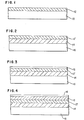
- a semiconductor substrate 10 such as silicon
- a thin silicon dioxide (SiO 2 ) layer 14 having a thickness on the order 3 to 50 nanometers.
- a mixture of a transition metal nitride such as for example HfN (plus Si 3 N 4 ) is deposited over the Si0 2 layer 14 and oxidized to convert the HfN/Si 3 N 4 mixture into a mixture of Hf0 2 /Si 3 N 4 12'.
- the presence of the Si0 2 layer 14 between the thin high dielectric constant nitride based insulator 12' is in order to further reduce the current leakage between the very thin insulator 12' and the substrate 10.
- the combined dielectric structure produced by layers 14 and 12' can be made very thin approximately in a range of 2 to 20 nanometers of SiO 2 equivalent, with a substantially higher dielectric constant and breakdown voltage characteristics.
- a conductive layer 16 made, for example, from doped (with a conductivity determining impurity) polycrystalline silicon, a metal silicide or a metal, deposited on dielectric layer 12' to form a capacitor having electrodes or plates 10 (wherein the substrate is doped to be conductive) and conductive layer 16 with the dielectric medium 18 composed of dielectric layer 14 and 12'.
- dielectric medium 18 having a dielectric constant which is several times greater than that of silicon dioxide and greater than that of silicon nitride, or silicon oxynitride. It also has a current leakage which is as good as any of a previously known structure. Furthermore, the dielectric medium 18 can withstand temperatures of 1,000°C and higher for long periods of time without adversely affecting its insulating index.
- a capacitor having the characteristics indicated hereinabove is particularly useful in semiconductor integrated circuits such as storage transistors or nodes in very dense memory systems.
- Fig. 4 there is shown a diagrammatic cross-sectional view of a structure such as that shown in Fig. 3, which further includes an additional dielectric layer 18, such as a layer of silicon nitride, between the transition metal oxide/silicon nitride layer 12' and electrode 16.
- an additional dielectric layer 18 such as a layer of silicon nitride, between the transition metal oxide/silicon nitride layer 12' and electrode 16.
- This layer further improves the dielectric properties of the dielectric medium of the capacitor.
- transition metal nitrides such as those made of tantalum (Ta), zirconium (Zr), titanium (Ti), yttrium (Y) and the rare earth elements [lanthanum (La) through lutetium (Lu)], may also be used.
- a mixture layer 12' is produced, which includes tantalum pentoxide (Ta 2 0 5 ) and silicon nitride.
- the layer 12 in Fig. 1 may include any mixture of a transition metal nitride and silicon nitride having about 25% to 55% transition metal nitride by atomic volume so that layer 12' comprises a mixture which includes an oxide of the transition metal and silicon nitride.
- hafnium oxide has a leakage which is about 100,000 times that of silicon dioxide and, furthermore, hafnium oxide cannot withstand temperatures higher than 400°C to 500°C without adversely affecting its insulating quality. Accordingly, when hafnium oxide is used in semiconductor integrated circuits, it must be formed late in the integrated circuit process after all hot process steps have been performed.
- the current leakage is considerably decreased from that found in dielectric material using transition metal oxides alone.
- the current leakage is further improved by using the dual layer dielectric of the present invention as shown in Fig. 3.
- substrate 10 in Figs. 1 and 2 was indicated as being made of a semiconductor material, such as silicon, it should be understood that the substrate 10 may also be made of some other conductive or insulating material as long as the material is oxidation resistant. However, if the dielectric structure is to be used as the dielectric medium of a capacitor, then substrate 10 should be a doped semiconductor material or some other conductive material suitable for forming capacitor electrodes.
- a novel dielectric mixture for a capacitor which is made by oxidizing a layer of a mixture of a transition metal nitride and silicon nitride.
- the preferred range for the transition metal nitride in the mixture is about 25% to 55% with the remaining made up of silicon nitride.
- the transition metal nitride and the silicon nitride are deposited onto a substrate, which may be made of a semiconductor, conductor or insulator material.
- the structure is then oxidized, preferably in dry oxygen, although wet oxygen may also be used, at a temperature which is preferably 800°C or higher for several minutes or longer until all of the transition metal nitride in the mixture is converted into a transition metal oxide.
- the new mixture of transition metal oxide and silicon nitride preferably has a thickness of 5 to 50 nanometers.
- the new mixture may be patterned by known etchants, e.g., techniques used with dry or wet etching processes for patterning silicon nitride layers. If the substrate is a conductor.,- then an electrically conductive layer, which may be made of doped polysilicon, a silicide or a metal, can be deposited onto the dielectric mixture to produce a high dielectric constant low leakage capacitor.
- a homogeneous transition metal oxide/silicon nitride mixture may also be directly formed during deposition, by use of known reactive sputtering or reactive evaporation techniques or chemical vapor deposition.
- the nitride mixture derived from the above indicated techniques should be subsequently heated within an oxygen atmosphere under the same temperature conditions identified hereinabove.
- a capacitor including a dielectric medium having a high quality index i.e., high dielectric constant and low current leakage, particularly suitable for use in dense integrated memory circuits, has been provided by employing a simple fabrication process.
- the dielectric medium may be produced at any stage during the making of semiconductor integrated circuits since the dielectric medium can readily withstand and is stable at high temperatures of more than 1000°C without destroying the high quality index of the dielectric medium.
Landscapes
- Engineering & Computer Science (AREA)
- Power Engineering (AREA)
- Manufacturing & Machinery (AREA)
- Microelectronics & Electronic Packaging (AREA)
- Semiconductor Integrated Circuits (AREA)
- Fixed Capacitors And Capacitor Manufacturing Machines (AREA)
- Formation Of Insulating Films (AREA)
- Insulated Gate Type Field-Effect Transistor (AREA)
Applications Claiming Priority (2)
| Application Number | Priority Date | Filing Date | Title |
|---|---|---|---|
| US527454 | 1983-08-29 | ||
| US06/527,454 US4464701A (en) | 1983-08-29 | 1983-08-29 | Process for making high dielectric constant nitride based materials and devices using the same |
Publications (3)
| Publication Number | Publication Date |
|---|---|
| EP0137196A2 true EP0137196A2 (fr) | 1985-04-17 |
| EP0137196A3 EP0137196A3 (en) | 1987-08-19 |
| EP0137196B1 EP0137196B1 (fr) | 1988-12-28 |
Family
ID=24101530
Family Applications (1)
| Application Number | Title | Priority Date | Filing Date |
|---|---|---|---|
| EP84109401A Expired EP0137196B1 (fr) | 1983-08-29 | 1984-08-08 | Procédé de fabrication de matériaux à haute constante diélectrique à base de nitrure et dispositifs l'utilisant |
Country Status (4)
| Country | Link |
|---|---|
| US (1) | US4464701A (fr) |
| EP (1) | EP0137196B1 (fr) |
| JP (1) | JPS6050950A (fr) |
| DE (1) | DE3475849D1 (fr) |
Families Citing this family (47)
| Publication number | Priority date | Publication date | Assignee | Title |
|---|---|---|---|---|
| US4464701A (en) * | 1983-08-29 | 1984-08-07 | International Business Machines Corporation | Process for making high dielectric constant nitride based materials and devices using the same |
| JP2617457B2 (ja) * | 1985-11-29 | 1997-06-04 | 株式会社日立製作所 | 半導体装置およびその製造方法 |
| EP0421487A3 (en) * | 1986-05-20 | 1991-07-24 | Showa Denko Kabushiki Kaisha | Solid electrolytic capacitor |
| JPH01225149A (ja) * | 1988-03-04 | 1989-09-08 | Toshiba Corp | キャパシタ及びその製造方法 |
| US4931897A (en) * | 1989-08-07 | 1990-06-05 | Mitsubishi Denki Kabushiki Kaisha | Method of manufacturing semiconductor capacitive element |
| JP2559079Y2 (ja) * | 1991-06-28 | 1998-01-14 | 科学技術庁放射線医学総合研究所長 | ピペッティング器具 |
| US5208789A (en) * | 1992-04-13 | 1993-05-04 | Lectret S. A. | Condenser microphones based on silicon with humidity resistant surface treatment |
| US6447838B1 (en) * | 1993-12-10 | 2002-09-10 | Symetrix Corporation | Integrated circuit capacitors with barrier layer and process for making the same |
| US5590017A (en) * | 1995-04-03 | 1996-12-31 | Aluminum Company Of America | Alumina multilayer wiring substrate provided with high dielectric material layer |
| US5786248A (en) * | 1995-10-12 | 1998-07-28 | Micron Technology, Inc. | Semiconductor processing method of forming a tantalum oxide containing capacitor |
| US5843830A (en) * | 1996-06-26 | 1998-12-01 | Micron Technology, Inc. | Capacitor, and methods for forming a capacitor |
| US6331680B1 (en) | 1996-08-07 | 2001-12-18 | Visteon Global Technologies, Inc. | Multilayer electrical interconnection device and method of making same |
| US6251720B1 (en) | 1996-09-27 | 2001-06-26 | Randhir P. S. Thakur | High pressure reoxidation/anneal of high dielectric constant materials |
| US5876788A (en) * | 1997-01-16 | 1999-03-02 | International Business Machines Corporation | High dielectric TiO2 -SiN composite films for memory applications |
| US5910880A (en) * | 1997-08-20 | 1999-06-08 | Micron Technology, Inc. | Semiconductor circuit components and capacitors |
| US5945203A (en) * | 1997-10-14 | 1999-08-31 | Zms Llc | Stratified composite dielectric and method of fabrication |
| US6911371B2 (en) | 1997-12-19 | 2005-06-28 | Micron Technology, Inc. | Capacitor forming methods with barrier layers to threshold voltage shift inducing material |
| US6165833A (en) * | 1997-12-19 | 2000-12-26 | Micron Technology, Inc. | Semiconductor processing method of forming a capacitor |
| US6085413A (en) * | 1998-02-02 | 2000-07-11 | Ford Motor Company | Multilayer electrical interconnection device and method of making same |
| US6162744A (en) * | 1998-02-28 | 2000-12-19 | Micron Technology, Inc. | Method of forming capacitors having high-K oxygen containing capacitor dielectric layers, method of processing high-K oxygen containing dielectric layers, method of forming a DRAM cell having having high-K oxygen containing capacitor dielectric layers |
| US6191443B1 (en) | 1998-02-28 | 2001-02-20 | Micron Technology, Inc. | Capacitors, methods of forming capacitors, and DRAM memory cells |
| US6156638A (en) | 1998-04-10 | 2000-12-05 | Micron Technology, Inc. | Integrated circuitry and method of restricting diffusion from one material to another |
| US6730559B2 (en) | 1998-04-10 | 2004-05-04 | Micron Technology, Inc. | Capacitors and methods of forming capacitors |
| US6165834A (en) * | 1998-05-07 | 2000-12-26 | Micron Technology, Inc. | Method of forming capacitors, method of processing dielectric layers, method of forming a DRAM cell |
| US6255186B1 (en) | 1998-05-21 | 2001-07-03 | Micron Technology, Inc. | Methods of forming integrated circuitry and capacitors having a capacitor electrode having a base and a pair of walls projecting upwardly therefrom |
| JP2000208508A (ja) * | 1999-01-13 | 2000-07-28 | Texas Instr Inc <Ti> | 珪酸塩高誘電率材料の真空蒸着 |
| US6737716B1 (en) | 1999-01-29 | 2004-05-18 | Kabushiki Kaisha Toshiba | Semiconductor device and method of manufacturing the same |
| KR100376264B1 (ko) * | 1999-12-24 | 2003-03-17 | 주식회사 하이닉스반도체 | 게이트 유전체막이 적용되는 반도체 소자의 제조 방법 |
| US6319766B1 (en) | 2000-02-22 | 2001-11-20 | Applied Materials, Inc. | Method of tantalum nitride deposition by tantalum oxide densification |
| US7005695B1 (en) * | 2000-02-23 | 2006-02-28 | Micron Technology, Inc. | Integrated circuitry including a capacitor with an amorphous and a crystalline high K capacitor dielectric region |
| EP1150350A3 (fr) * | 2000-02-25 | 2002-04-24 | Infineon Technologies North America Corp. | Fabrication d'un condensateur en tranchée |
| JP3786566B2 (ja) * | 2000-06-27 | 2006-06-14 | 株式会社東芝 | 半導体装置及びその製造方法 |
| US6576967B1 (en) | 2000-09-18 | 2003-06-10 | Motorola, Inc. | Semiconductor structure and process for forming a metal oxy-nitride dielectric layer |
| JP4104834B2 (ja) * | 2001-04-13 | 2008-06-18 | 株式会社東芝 | Mis型電界効果トランジスタの製造方法 |
| US7037862B2 (en) * | 2001-06-13 | 2006-05-02 | Micron Technology, Inc. | Dielectric layer forming method and devices formed therewith |
| US6642147B2 (en) * | 2001-08-23 | 2003-11-04 | International Business Machines Corporation | Method of making thermally stable planarizing films |
| CN100468638C (zh) | 2001-12-18 | 2009-03-11 | 松下电器产业株式会社 | 半导体元件的制造方法 |
| US6898070B2 (en) * | 2002-12-19 | 2005-05-24 | Avx Corporation | Transmission line capacitor |
| US6812110B1 (en) | 2003-05-09 | 2004-11-02 | Micron Technology, Inc. | Methods of forming capacitor constructions, and methods of forming constructions comprising dielectric materials |
| US20060054595A1 (en) * | 2004-09-10 | 2006-03-16 | Honeywell International Inc. | Selective hafnium oxide etchant |
| US7531405B2 (en) * | 2005-02-28 | 2009-05-12 | Qimonds Ag | Method of manufacturing a dielectric layer and corresponding semiconductor device |
| DE102006041738A1 (de) * | 2006-09-04 | 2008-03-06 | Leibniz-Institut Für Neue Materialien Gemeinnützige Gmbh | Zusammensetzung zur Beschichtung elektrischer Leiter und Verfahren zur Herstellung einer solchen Zusammensetzung |
| JP4523995B2 (ja) * | 2009-11-26 | 2010-08-11 | キヤノンアネルバ株式会社 | 電界効果トランジスタの製造方法 |
| JP4523994B2 (ja) * | 2009-11-26 | 2010-08-11 | キヤノンアネルバ株式会社 | 電界効果トランジスタの製造方法 |
| CN103970374A (zh) * | 2013-01-28 | 2014-08-06 | 宸鸿科技(厦门)有限公司 | 触控单元及触控面板 |
| US10164003B2 (en) | 2016-01-14 | 2018-12-25 | Taiwan Semiconductor Manufacturing Company Ltd. | MIM capacitor and method of forming the same |
| US9853025B1 (en) * | 2016-10-14 | 2017-12-26 | International Business Machines Corporation | Thin film metallic resistors formed by surface treatment of insulating layer |
Family Cites Families (8)
| Publication number | Priority date | Publication date | Assignee | Title |
|---|---|---|---|---|
| US2960642A (en) * | 1958-04-17 | 1960-11-15 | Quartz & Silice S A | Dielectric films and capacitors employing the same |
| DE1120023B (de) * | 1958-04-17 | 1961-12-21 | Andre De Rudnay | Verfahren zur Herstellung eines aus Titandioxyd bestehenden Dielektrikums fuer Kondensatoren |
| US3786323A (en) * | 1972-07-03 | 1974-01-15 | Bell Telephone Labor Inc | Capacitor with anodized electrode of tantalum silicon alloy |
| JPS54133089A (en) * | 1978-04-06 | 1979-10-16 | Nec Corp | Thin film capacitor and its manufacture |
| JPS56147470A (en) * | 1980-04-17 | 1981-11-16 | Nec Corp | Semiconductor device |
| JPS5745968A (en) * | 1980-08-29 | 1982-03-16 | Ibm | Capacitor with double dielectric unit |
| US4432035A (en) * | 1982-06-11 | 1984-02-14 | International Business Machines Corp. | Method of making high dielectric constant insulators and capacitors using same |
| US4464701A (en) * | 1983-08-29 | 1984-08-07 | International Business Machines Corporation | Process for making high dielectric constant nitride based materials and devices using the same |
-
1983
- 1983-08-29 US US06/527,454 patent/US4464701A/en not_active Expired - Lifetime
-
1984
- 1984-04-19 JP JP59077670A patent/JPS6050950A/ja active Pending
- 1984-08-08 EP EP84109401A patent/EP0137196B1/fr not_active Expired
- 1984-08-08 DE DE8484109401T patent/DE3475849D1/de not_active Expired
Also Published As
| Publication number | Publication date |
|---|---|
| US4464701A (en) | 1984-08-07 |
| EP0137196A3 (en) | 1987-08-19 |
| JPS6050950A (ja) | 1985-03-22 |
| EP0137196B1 (fr) | 1988-12-28 |
| DE3475849D1 (en) | 1989-02-02 |
Similar Documents
| Publication | Publication Date | Title |
|---|---|---|
| EP0137196B1 (fr) | Procédé de fabrication de matériaux à haute constante diélectrique à base de nitrure et dispositifs l'utilisant | |
| US4432035A (en) | Method of making high dielectric constant insulators and capacitors using same | |
| US6075691A (en) | Thin film capacitors and process for making them | |
| US5349494A (en) | Semiconductor device with capacitor insulating film and method for fabricating the same | |
| KR920005320B1 (ko) | 캐패시터 및 그 제조방법 | |
| US4996081A (en) | Method of forming multiple nitride coating on silicon | |
| JP2893009B2 (ja) | メモリ・アプリケーション用の絶縁性の高い複合薄膜 | |
| US6461931B1 (en) | Thin dielectric films for DRAM storage capacitors | |
| EP0072603B1 (fr) | Procédé de fabrication d'un dispositif semiconducteur muni d'une couche isolante de dioxyde de silicium couverte d'une couche d'oxynitrure de silicium | |
| US4891684A (en) | Semiconductor device | |
| CA1159917A (fr) | Structure de condensateur avec double dielectrique | |
| US6734068B2 (en) | Method to form silicates as high dielectric constant materials | |
| JP2001077111A (ja) | アルミニウムをドープしたジルコニウム誘電体膜のトランジスタ構造およびその堆積方法 | |
| JPS6010773A (ja) | 1素子型fet−記憶キヤパシタ回路の形成方法 | |
| JPH04279053A (ja) | 高値タンタル酸化物コンデンサ | |
| JPS60153158A (ja) | キャパシタ誘電体膜の製造方法 | |
| US6468856B2 (en) | High charge storage density integrated circuit capacitor | |
| US6171941B1 (en) | Method for fabricating capacitor of semiconductor memory device using titanium aluminum nitride as diffusion-inhibiting layer | |
| JPS6128213B2 (fr) | ||
| JPH06275776A (ja) | キャパシタ | |
| KR100373819B1 (ko) | 캐패시터및박막캐패시터제조방법 | |
| JPS5984570A (ja) | 半導体装置用キヤパシタの製造方法 | |
| JPH0260157A (ja) | 半導体装置 | |
| JPS6242392B2 (fr) | ||
| KR100305719B1 (ko) | 하부 전하저장 전극 형성 방법 |
Legal Events
| Date | Code | Title | Description |
|---|---|---|---|
| PUAI | Public reference made under article 153(3) epc to a published international application that has entered the european phase |
Free format text: ORIGINAL CODE: 0009012 |
|
| 17P | Request for examination filed |
Effective date: 19841123 |
|
| AK | Designated contracting states |
Designated state(s): DE FR GB |
|
| XX | Miscellaneous (additional remarks) |
Free format text: DIE MELDUNG VOM 850508 BEZOG SICH AUF 138998 |
|
| EL | Fr: translation of claims filed | ||
| PUAL | Search report despatched |
Free format text: ORIGINAL CODE: 0009013 |
|
| AK | Designated contracting states |
Kind code of ref document: A3 Designated state(s): DE FR GB |
|
| 17Q | First examination report despatched |
Effective date: 19871105 |
|
| GRAA | (expected) grant |
Free format text: ORIGINAL CODE: 0009210 |
|
| AK | Designated contracting states |
Kind code of ref document: B1 Designated state(s): DE FR GB |
|
| REF | Corresponds to: |
Ref document number: 3475849 Country of ref document: DE Date of ref document: 19890202 |
|
| ET | Fr: translation filed | ||
| PLBE | No opposition filed within time limit |
Free format text: ORIGINAL CODE: 0009261 |
|
| STAA | Information on the status of an ep patent application or granted ep patent |
Free format text: STATUS: NO OPPOSITION FILED WITHIN TIME LIMIT |
|
| 26N | No opposition filed | ||
| PGFP | Annual fee paid to national office [announced via postgrant information from national office to epo] |
Ref country code: DE Payment date: 19940824 Year of fee payment: 11 |
|
| PGFP | Annual fee paid to national office [announced via postgrant information from national office to epo] |
Ref country code: FR Payment date: 19950807 Year of fee payment: 12 |
|
| PG25 | Lapsed in a contracting state [announced via postgrant information from national office to epo] |
Ref country code: DE Effective date: 19960501 |
|
| PGFP | Annual fee paid to national office [announced via postgrant information from national office to epo] |
Ref country code: GB Payment date: 19960724 Year of fee payment: 13 |
|
| PG25 | Lapsed in a contracting state [announced via postgrant information from national office to epo] |
Ref country code: FR Effective date: 19970430 |
|
| REG | Reference to a national code |
Ref country code: FR Ref legal event code: ST |
|
| PG25 | Lapsed in a contracting state [announced via postgrant information from national office to epo] |
Ref country code: GB Free format text: LAPSE BECAUSE OF NON-PAYMENT OF DUE FEES Effective date: 19970808 |
|
| GBPC | Gb: european patent ceased through non-payment of renewal fee |
Effective date: 19970808 |