EP0137462A2 - Integrierte Filterschaltung - Google Patents
Integrierte Filterschaltung Download PDFInfo
- Publication number
- EP0137462A2 EP0137462A2 EP84111944A EP84111944A EP0137462A2 EP 0137462 A2 EP0137462 A2 EP 0137462A2 EP 84111944 A EP84111944 A EP 84111944A EP 84111944 A EP84111944 A EP 84111944A EP 0137462 A2 EP0137462 A2 EP 0137462A2
- Authority
- EP
- European Patent Office
- Prior art keywords
- filter
- integrated
- trap
- circuit
- switching
- Prior art date
- Legal status (The legal status is an assumption and is not a legal conclusion. Google has not performed a legal analysis and makes no representation as to the accuracy of the status listed.)
- Withdrawn
Links
- 239000003990 capacitor Substances 0.000 claims description 9
- 238000010586 diagram Methods 0.000 description 9
- XUIMIQQOPSSXEZ-UHFFFAOYSA-N Silicon Chemical compound [Si] XUIMIQQOPSSXEZ-UHFFFAOYSA-N 0.000 description 3
- 239000004065 semiconductor Substances 0.000 description 3
- 229910052710 silicon Inorganic materials 0.000 description 3
- 239000010703 silicon Substances 0.000 description 3
- 238000010276 construction Methods 0.000 description 2
- 230000010354 integration Effects 0.000 description 2
- 239000000758 substrate Substances 0.000 description 2
- 238000010521 absorption reaction Methods 0.000 description 1
- 230000007547 defect Effects 0.000 description 1
- 230000014509 gene expression Effects 0.000 description 1
- 239000012535 impurity Substances 0.000 description 1
- 230000001788 irregular Effects 0.000 description 1
- 238000000034 method Methods 0.000 description 1
- 238000009966 trimming Methods 0.000 description 1
Images



Classifications
-
- H—ELECTRICITY
- H03—ELECTRONIC CIRCUITRY
- H03H—IMPEDANCE NETWORKS, e.g. RESONANT CIRCUITS; RESONATORS
- H03H11/00—Networks using active elements
- H03H11/02—Multiple-port networks
- H03H11/04—Frequency selective two-port networks
-
- H—ELECTRICITY
- H03—ELECTRONIC CIRCUITRY
- H03H—IMPEDANCE NETWORKS, e.g. RESONANT CIRCUITS; RESONATORS
- H03H11/00—Networks using active elements
- H03H11/02—Multiple-port networks
- H03H11/04—Frequency selective two-port networks
- H03H11/12—Frequency selective two-port networks using amplifiers with feedback
- H03H11/1295—Parallel-T filters
Definitions
- This invention relates to an integrated filter circuit suitable to be formed within a monolithic integrated circuit (monolithic IC) on a silicon wafer or the like.
- IC integrated circuits
- Most of the filters that have been used so far are formed of inductance L, capacitance C and resistance R. Since the inductance L is difficult to be integrated, active filters that can be formed of only capacitance C and resistance R are suitable for being formed as ICs.
- Fig. 1 shows a trap filter known as a Twin-T. In Fig. 1, if the resistances Rl, R2 and R3 and capacitances Cl, C2 and C3 are selected to have the relation given as the trap frequency fr can be expressed by In Fig. 1, v i represents an input signal and v is an output signal.
- the values of the capacitances and resistances within the IC are scattered by the irregular impurity concentration within the semiconductor and misregistration of masks.
- the value of capacitance C and that of resistance R have great variations within ⁇ 20% and ⁇ 15%, respectively. Therefore, the trap frequency of the trap filter of Fig. 1 changes within the range from a(f r ) to b(f r ') as shown in Fig. 2.
- the trap frequency f r deviates ⁇ 35%, under which the filter is extremely difficult for practical use.
- the resistances on the IC chip are adjusted in value by laser trimming so that the scattering of resistance can be absorbed. This method, however, cannot solve the problems of precision, yield and so on.
- an integrated filter circuit comprising a plurality of parallel-connected filter circuits each including resistances and capacitances in which at least either the resistances or the capacitances have different values, and means for selecting one of the parallel-connected filters whereby the scattering of the integrated capacitances and resistances can be absorbed.
- the use of variable capacitance diodes for the integrated capacitances can extend the range of absorbing the scattering and raise the precision.
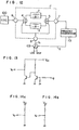
- the filter 3 includes resistors R4, R5 and R6 and capacitors C4, C5 and C6 of which the relative values are selected as
- the switching circuit 4 in Fig..3 corresponds to the block including transistors Q3 and Q4 and an inverter 9 and the switching circuit 5 in Fig. 3 corresponds to the block including transistors Q7 and Q8.
- the control signal v s is high level, the transistor Q3 is turned on and the transistor Q4 is turned off with the result that the input signal v i is supplied through the transistors Q2 and A6 to the filter 3.
- the trap frequency f r1 of the filter 2 is selected to be 15% lower than a desired value f
- the trap frequency f r2 of the filter 3 is 15% higher than the value f o as shown in Fig. 5, and either of the filters 2 and 3 is selected as follows, then the scattering can be limited to f o ⁇ 20%.
- the filter 2 when the trap frequency f trap is larger than the center value (trap frequency) f r1 of the filter 2, or f trap ⁇ f r1 , the filter 2 is selected, while when the trap frequency f trap is lower than the center value (trap frequency) f r2 of the filter 3, or f trap ⁇ f r2 , the filter 3 is selected.
- the way to select either of the filters 2 and 3 is, for example, shown in Fig. 12. That is, in Fig. 12, an oscillator 100 is connected to the input signal pin 6, a voltage level changing switch 103 to the control pin 8, and a frequency discriminator 101 between the output signal pin 7 and the switch 103.
- the switch 103 is responsive to an output g from the frequency discriminator 101 to changes to the fixed low-level side position for its low level or to the fixed high-level side position for its high level. At initial setting, when the output g is low level, or the control signal v s is low level, the filter 2 is selected.
- the switch 103 is constructed as, for example, shown in Fig. 13.
- the switch 103 When the control signal g is high level, the switch 103 is changed to the high level side position so that the control signal v s is high level to select the filter 3 .
- the frequencies f 1 and f 2 ' are thus within the range of target value f o ⁇ 20%.
- Fig. 6 it is extremely effective to form the capacitors Cl to C6 by variable capacitance diodes Dl to D6. Since pairs of elements can be formed with high precision within the IC, the voltage to be applied to the variable capacitance diodes Dl to D6 used for a plurality of filters can be changed by a single control voltage v . Shown at 10 is an IC pin through which the voltage v c is applied. In the example of Fig.
- the anode side potentials of the variable capacitance diodes Dl to D6 are set to be equal to the emitter voltage of the transistor Q5 or Q6,.and the cathode side potentials v c thereof are changed to change the voltages across the variable capacitance diodes, and hence the values of the capacitors Cl to C6.
- the base-emitter capacitances of the variable capacitance diodes can be expressed as where
- F ig. 7 shows an example of the characteristic.
- the V j can take a value in the range from 0 to 3 V, and C j can be changed within the range of typical value ⁇ 20%.
- all the scattering of the capacitance C and resistance R can be absorbed by using the variable capacitance diodes.
- Fig. 8 is a cross-sectional diagram of the IC, using base-emitter junction capacitances for variable capacitance diodes.
- n represents an n-type semiconductor (silicon) and P a p-type semiconductor (silicon).
- Numeral 11 represents an emitter, 12 a base, 13 a collector and 14 a substrate. Since the collector 13 is connected to the power supply, a capacitance C is present between the base 12 and the power supply in addition to the capacitance C j as shown in Fig. 9. Only the capacitance C. can be used as a variable capacitance diode, and the capacitance C s is necessary to be as small as possible relative to the capacitance C j .
- Figs. 10 and 11 show other embodiments of this invention. These embodiments are different from the embodiment of Fig. 3 in that only the switching circuit 4 is used in Fig. 10 and that only the switching circuit 5 is used in Fig. ll. Also in these cases, a signal passed through either filter 2 or filter 3 can be produced as the output v .
- Figs. 15 and 16 show other embodiments of this invention in which the filter characteristics are changed by switching over resistors or capacitors by means of the switching circuit 4. Further, resistor and capacitor switching may be jointly used for the change of filter characteristic. A variable capacitance element may be used as the capacitor.
- the base-emitter junction capacitance is used as a variable capacitance diode
- the base-collector junction capacitance, collector-substrate junction capacitance and so on can be used as variable-capacitance diodes.
- the scattering of the filter characteristics due to the scattering of the elements of an IC can be absorbed by providing a plurality of parallel filter circuits of resistances and capacitances in which at least either resistances or capacitances are different in values and switching means for switching these parallel filter circuits, or by providing a single filter circuit and switching resistors or capacitors in the filter circuit by a switch, and by using the base-emitter junction capacitances as variable capacitance diodes within the IC.
- This invention can be applied not only to the trap filter mentioned in the above embodiments but also to all types of filters formed by resistors and capacitors.
- a large-sized block filter which has been used as a discrete component so far can be formed as an IC, thus leading to low-cost and small-sized circuits and small number of parts to be used.
Landscapes
- Networks Using Active Elements (AREA)
- Filters And Equalizers (AREA)
Applications Claiming Priority (2)
| Application Number | Priority Date | Filing Date | Title |
|---|---|---|---|
| JP58186776A JPS6090411A (ja) | 1983-10-07 | 1983-10-07 | フイルタ集積回路 |
| JP186776/83 | 1983-10-07 |
Publications (2)
| Publication Number | Publication Date |
|---|---|
| EP0137462A2 true EP0137462A2 (de) | 1985-04-17 |
| EP0137462A3 EP0137462A3 (de) | 1986-10-08 |
Family
ID=16194409
Family Applications (1)
| Application Number | Title | Priority Date | Filing Date |
|---|---|---|---|
| EP84111944A Withdrawn EP0137462A3 (de) | 1983-10-07 | 1984-10-05 | Integrierte Filterschaltung |
Country Status (3)
| Country | Link |
|---|---|
| US (1) | US4724407A (de) |
| EP (1) | EP0137462A3 (de) |
| JP (1) | JPS6090411A (de) |
Cited By (2)
| Publication number | Priority date | Publication date | Assignee | Title |
|---|---|---|---|---|
| EP0273365A3 (en) * | 1986-12-27 | 1990-09-26 | Sony Corporation | Filter adjustment apparatus and method |
| EP0427105A1 (de) * | 1989-11-07 | 1991-05-15 | MARELLI AUTRONICA S.p.A. | Schaltung zur Verarbeitung des Signals, das von einem elektromagnetischen Rotationssensor erzeugt wird |
Families Citing this family (14)
| Publication number | Priority date | Publication date | Assignee | Title |
|---|---|---|---|---|
| JPH0773179B2 (ja) * | 1986-08-01 | 1995-08-02 | ロ−ム株式会社 | 微分回路 |
| JP2745417B2 (ja) * | 1989-02-16 | 1998-04-28 | 株式会社リコー | ファクシミリ装置 |
| US5142255A (en) * | 1990-05-07 | 1992-08-25 | The Texas A&M University System | Planar active endfire radiating elements and coplanar waveguide filters with wide electronic tuning bandwidth |
| JPH04299610A (ja) * | 1991-03-27 | 1992-10-22 | Rohm Co Ltd | フィルタ装置 |
| US5528682A (en) * | 1995-01-30 | 1996-06-18 | Harris Corporation | Double duty capacitor circuit and method |
| US5859908A (en) * | 1996-03-28 | 1999-01-12 | At&T Corp. | Method and apparatus for applying multiple speech processing features to a telephone call |
| US5673003A (en) * | 1996-03-29 | 1997-09-30 | Motorola, Inc. | Amplifier circuit having a variable bandwidth |
| US6167246A (en) * | 1997-05-09 | 2000-12-26 | Micrel Incorporated | Fully integrated all-CMOS AM receiver |
| JP3411016B2 (ja) * | 2000-12-01 | 2003-05-26 | 株式会社東芝 | フィルタ回路 |
| US7596195B2 (en) * | 2004-03-31 | 2009-09-29 | Broadcom Corporation | Bandpass filter with reversible IQ polarity to enable a high side or low side injection receiver architecture |
| US7603098B2 (en) * | 2004-03-31 | 2009-10-13 | Broadcom Corporation | Programmable IF frequency filter for enabling a compromise between DC offset rejection and image rejection |
| CN101390248B (zh) * | 2004-12-09 | 2012-12-05 | 维斯普瑞公司 | 零极点元件及相关系统和方法 |
| DE102005046445B4 (de) * | 2005-09-28 | 2019-10-10 | Snaptrack, Inc. | Bandpassfilter |
| US8112059B2 (en) * | 2009-09-16 | 2012-02-07 | Mediatek Singapore Pte. Ltd. | Mixer circuit, integrated circuit device and radio frequency communication unit |
Family Cites Families (12)
| Publication number | Priority date | Publication date | Assignee | Title |
|---|---|---|---|---|
| US3411098A (en) * | 1965-10-22 | 1968-11-12 | Halliburton Co | Variable q notched filter |
| DE1296226C2 (de) * | 1967-12-09 | 1978-03-16 | Philips" Patentverwaltung GmbH, 2000 Hamburg | Abstimm-schaltungsanordnung mit einer schaltdiode |
| US3533020A (en) * | 1969-01-13 | 1970-10-06 | Us Air Force | Reduction of intermodulation in varactor-tuned filters |
| DE1923893A1 (de) * | 1969-05-09 | 1970-11-19 | Siemens Ag | Bandfilter in der Art eines N-Pfad-Filters |
| US3582835A (en) * | 1969-07-28 | 1971-06-01 | Oak Electro Netics Corp | Filter switching circuit |
| US3742395A (en) * | 1970-10-21 | 1973-06-26 | Nippon Columbia | Variable bandwidth apparatus for transmission system |
| US4197515A (en) * | 1977-10-05 | 1980-04-08 | Gafvert Karl O U | Synchronous filter |
| FR2448250A1 (fr) * | 1979-02-02 | 1980-08-29 | Commissariat Energie Atomique | Filtre suiveur a commutation |
| FR2460564A1 (fr) * | 1979-06-29 | 1981-01-23 | Commissariat Energie Atomique | Ensemble de filtrage par commutation |
| US4302738A (en) * | 1980-04-11 | 1981-11-24 | Tektronix, Inc. | Noise rejection circuitry for a frequency discriminator |
| US4480338A (en) * | 1982-03-01 | 1984-10-30 | Zenith Electronics Corporation | Lowpass-highpass electronic switch |
| US4580161A (en) * | 1982-11-22 | 1986-04-01 | Pico Products, Inc. | Cable television subscriber control system including addressable filters having a variable pole |
-
1983
- 1983-10-07 JP JP58186776A patent/JPS6090411A/ja active Pending
-
1984
- 1984-10-05 EP EP84111944A patent/EP0137462A3/de not_active Withdrawn
-
1986
- 1986-05-14 US US06/863,244 patent/US4724407A/en not_active Expired - Fee Related
Cited By (2)
| Publication number | Priority date | Publication date | Assignee | Title |
|---|---|---|---|---|
| EP0273365A3 (en) * | 1986-12-27 | 1990-09-26 | Sony Corporation | Filter adjustment apparatus and method |
| EP0427105A1 (de) * | 1989-11-07 | 1991-05-15 | MARELLI AUTRONICA S.p.A. | Schaltung zur Verarbeitung des Signals, das von einem elektromagnetischen Rotationssensor erzeugt wird |
Also Published As
| Publication number | Publication date |
|---|---|
| US4724407A (en) | 1988-02-09 |
| JPS6090411A (ja) | 1985-05-21 |
| EP0137462A3 (de) | 1986-10-08 |
Similar Documents
| Publication | Publication Date | Title |
|---|---|---|
| US4724407A (en) | Integrated filter circuit having switchable selected parallel filter paths | |
| US3535532A (en) | Integrated circuit including light source,photodiode and associated components | |
| CA1128670A (en) | Semiconductor device having a mos-capacitor | |
| US3953875A (en) | Capacitor structure and circuit facilitating increased frequency stability of integrated circuits | |
| US3860836A (en) | Stabilization of emitter followers | |
| JPH045289B2 (de) | ||
| US4801867A (en) | Monolithic microwave integrated circuit with probing pads | |
| US4314152A (en) | Monolithically integrable semiconductor circuit with an amplifier controlled by a photo diode | |
| US5760642A (en) | Filter circuit using a junction capacitor of a semiconductor | |
| US5475327A (en) | Variable impedance circuit | |
| US5091689A (en) | Constant current circuit and integrated circuit having said circuit | |
| US3725754A (en) | Transistor circuit of compound connection | |
| US5382837A (en) | Switching circuit for semiconductor device | |
| EP0396167B1 (de) | Schutzeinrichtung gegen den Durchbruch bipolarer Transistoren in einem integrierten Treiber-Schaltkreis für ein Leistungsbauelement mit resonanter Ladung am Kollektor | |
| US3914622A (en) | Latch circuit with noise suppression | |
| US4701638A (en) | Antisaturation circuit for integrated PNP transistor | |
| CA1132203A (en) | Frequency divider | |
| JPH05167017A (ja) | 半導体集積回路装置 | |
| EP0346978A1 (de) | Integrierte Stromspiegelschaltung mit vertikalen Transistoren | |
| EP0760165B1 (de) | Elektronische anordnung mit mitteln zum kompensieren von parasitären kapazitäten | |
| JP3373267B2 (ja) | Lc素子及び半導体装置 | |
| JPH10247846A (ja) | 入力回路 | |
| JPS60229415A (ja) | フイルタ集積回路 | |
| DE19532990C1 (de) | Integrierte Halbleiteranordnung mit einem NPN-Transistor in Basisschaltung | |
| JPH0462492B2 (de) |
Legal Events
| Date | Code | Title | Description |
|---|---|---|---|
| PUAI | Public reference made under article 153(3) epc to a published international application that has entered the european phase |
Free format text: ORIGINAL CODE: 0009012 |
|
| 17P | Request for examination filed |
Effective date: 19841005 |
|
| AK | Designated contracting states |
Designated state(s): DE FR GB |
|
| PUAL | Search report despatched |
Free format text: ORIGINAL CODE: 0009013 |
|
| AK | Designated contracting states |
Kind code of ref document: A3 Designated state(s): DE FR GB |
|
| 17Q | First examination report despatched |
Effective date: 19890217 |
|
| STAA | Information on the status of an ep patent application or granted ep patent |
Free format text: STATUS: THE APPLICATION HAS BEEN WITHDRAWN |
|
| 18W | Application withdrawn |
Withdrawal date: 19910423 |
|
| R18W | Application withdrawn (corrected) |
Effective date: 19910423 |
|
| RIN1 | Information on inventor provided before grant (corrected) |
Inventor name: OKADA, YOSHINORI Inventor name: KUDO, MITSURU Inventor name: FUKUSHIMA, ISAO Inventor name: KUBOTA, TAKASHI Inventor name: MIURA, KUNIAKI |